Board design
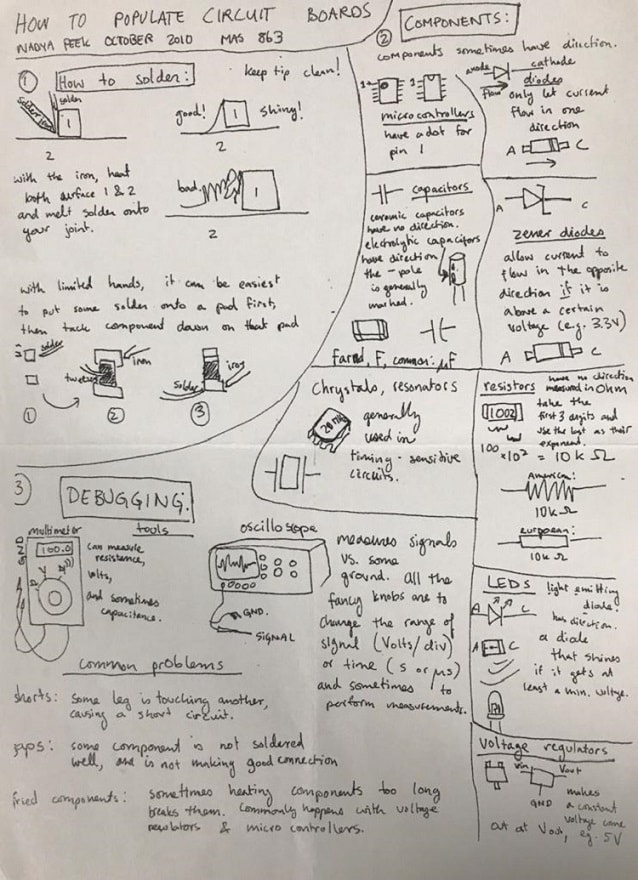
Initially, before any move to design the board and using the software, the instructor Wendy gave us a session or class about the electronics as we were given a sheet explaining components used in the electronic circuit board with drawing symbols.
This sheet which provided by Wendy, I had one but unfortunately, I lost mine somewhere in the lab and I used the one belongs to my colleague Salama.
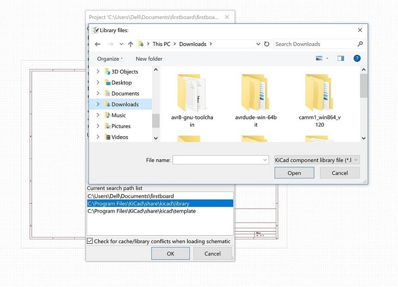
 Moving to download KiCad software from the given website KiCad and then downloading the library from the fabacademy site library
Im using the Echo Hello board for Neil, and I added these components to make new board.
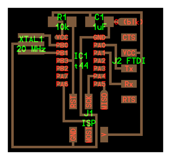
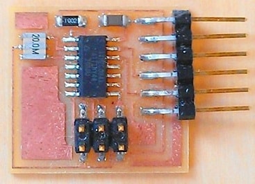
So the components that I added to the board were only three things which are the minimum of the assignment of this week:
1. Button
2. LED
3. Resistor.
And here is the full list of the my pcb components:
6-pin header
ATtiny44A
FTDI header
20MHz crystal
Capacitor (1uF)
1 Resistor (499k)
Button
LED
- Create a new project and new schematic in KiCad
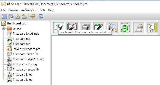
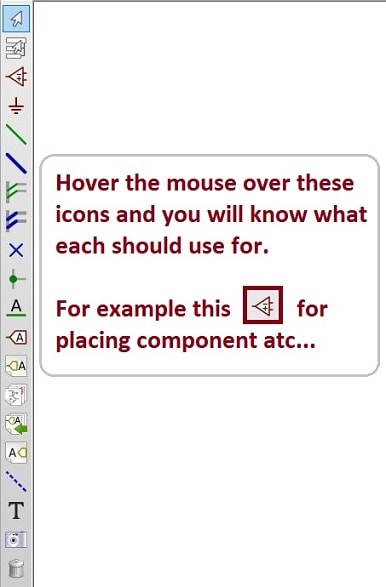
- Add components
This is my board "schematic" and all components connected.
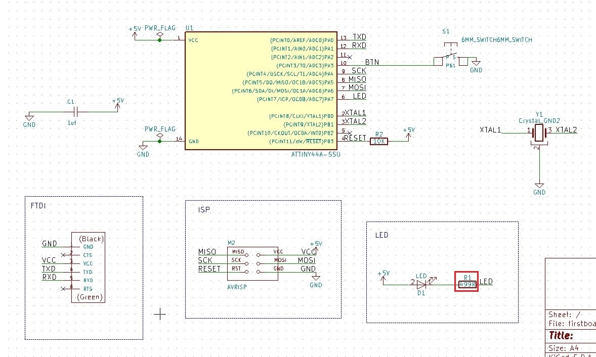
Why I choose the value of "499R" resistor?
We have excellent electronic engineers in our fablab,
Hashem
and Salama
I learned a lot from them, where how to calculate the values and on what basis I choose the specific resistor for LED as an example.
Well, regarding to Ohm's law, to calculate the value of Resistor we use this law
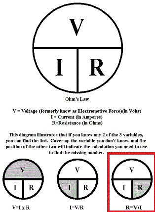
for a reference this image is taken from here
I am going to use the last equation to find the resistor value to use for my LED RGB.
Steps for this first I have to take the information from the datasheet for the LED So I do this:
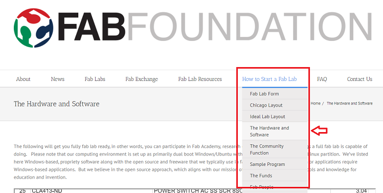


Here you can have the link for the datasheet
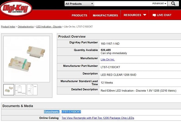
Finding the maximum red current from datasheet
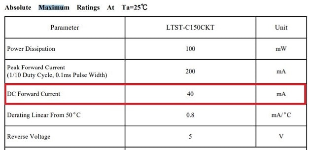
So the current is 40 here. And now we have to find the maximum voltage but first we need to know what Attiny we are using. It is ATtiny44A and from datasheet of

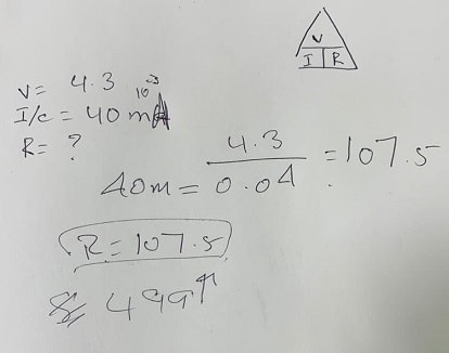
the result of equation is 107.5 which is the closest value that we have is 499K. and that’s why the one I used in the board have the value of 499K.
And this image shows the calculation of the equation.
Then after you add the components, connections, rewiring, board and alerts checking, means you use these tools after schematic to check the design of the board.

Listing the tools in order as the following:
1. Annotate schematic components
2. Perform electronic rules check
3. Generate netlist
4. Run CvPcb to associate components and footprints.
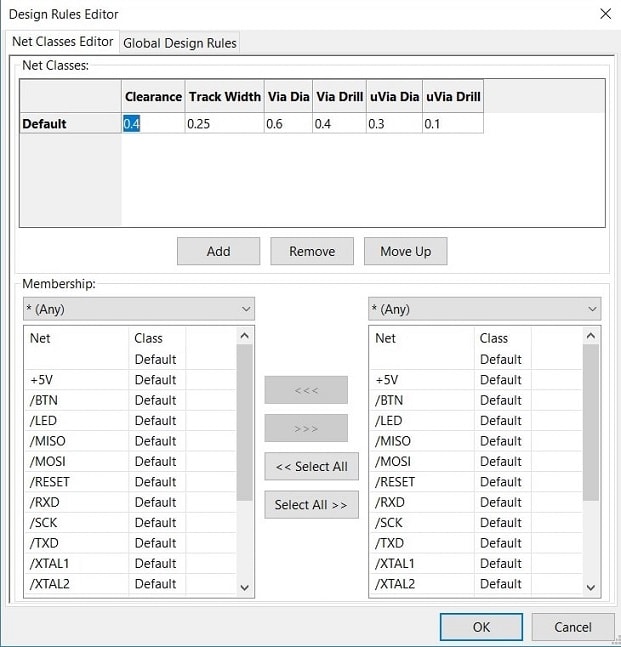
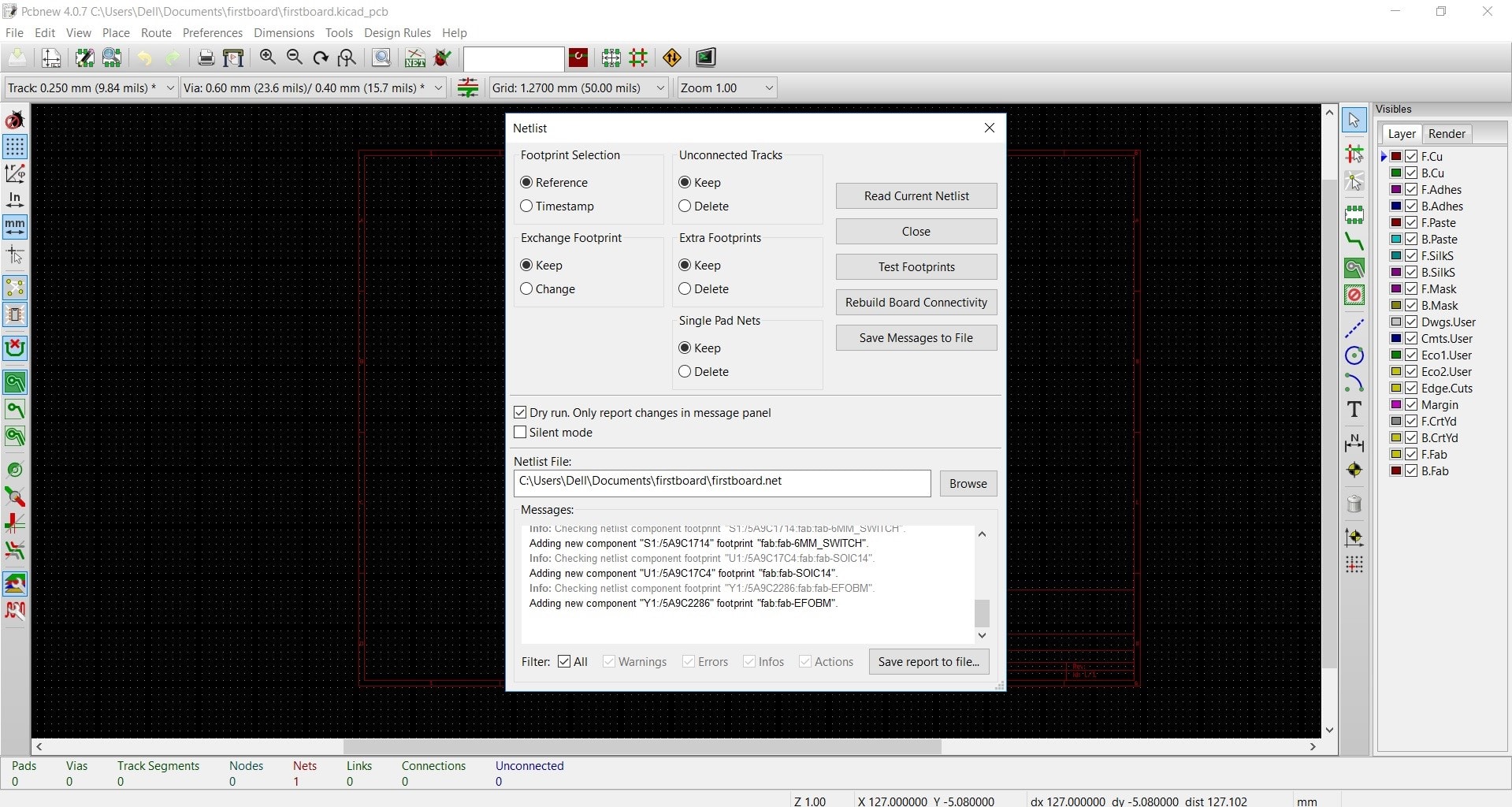
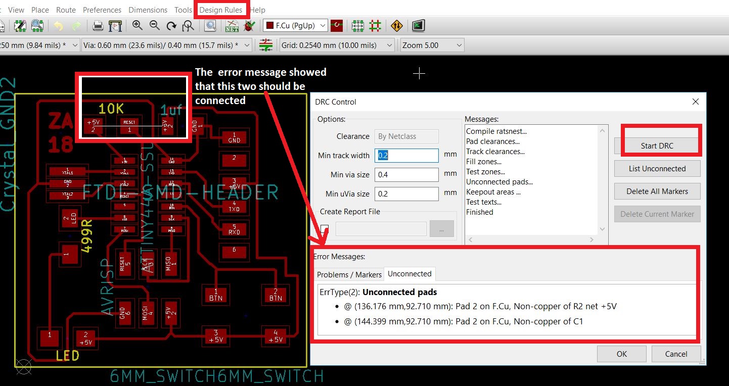
Open the DRC rules from the Design Rules menu.

This shows the error I had in the board 5V is not connected. If I did this before I cut the board I will not have to put a jumper to connect this two lines.
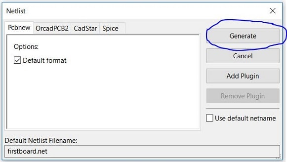
To generate the netlist
So as you can see in below image I'm creating the traces by connecting the pads. You know how they are connected because they are already linked with white. The red lines are the traces I've already drawn and the white ones those which needed to be drawn and I can do a better job in coming weeks. Also, as you can see the sidebar I ticked only the copper layer and edge cuts to show these 2 options and hide the rest because its hard to create or draw the traces with all layers shown.
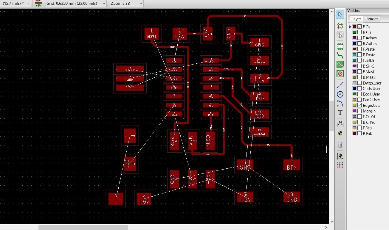
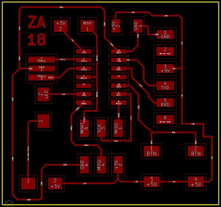
between these two images above and bottom the differences are clear after I finished drawing the board,
1. I did rotate the resistor 10K at the top of the board as you can see to make the better route for the trace.
2. I moved the location of the LED closer to the pin.
So, after finishing drawing the traces I can see more ways to draw them and I will do that in the coming weeks. And I want to mention the logo I did on my board. It was super awesome because as I scratched the logo on my fabISP and this time I did it digitally.
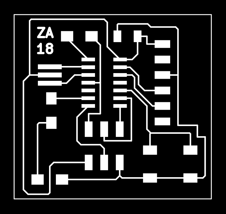
I save the file PNG type of file. In Paint, I save the trace and outline separately.
The trace "should be in white color" and the outline or the cut "should be black" also the resolution of the image should be 1000 up to 2000.
Both have to be saved in separate files.
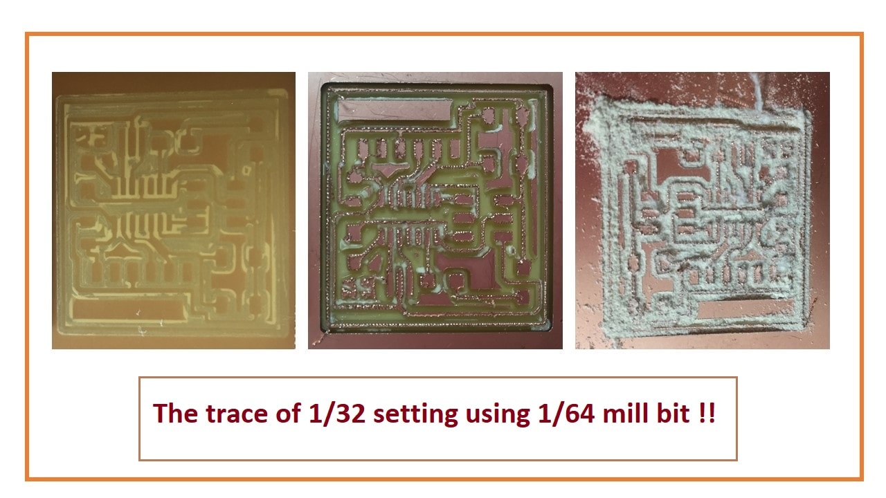
Well, you have to cut this in order, first you cut the traces then the outline so I used the wrong mill bit the first time! and you will see the images below what I mean.
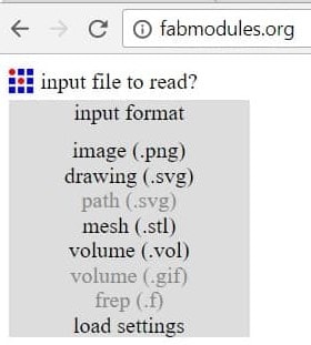
Through fabmodule here you can generate the "CAM" file.
1. Image (.png)
2. Roland mill (.rml)
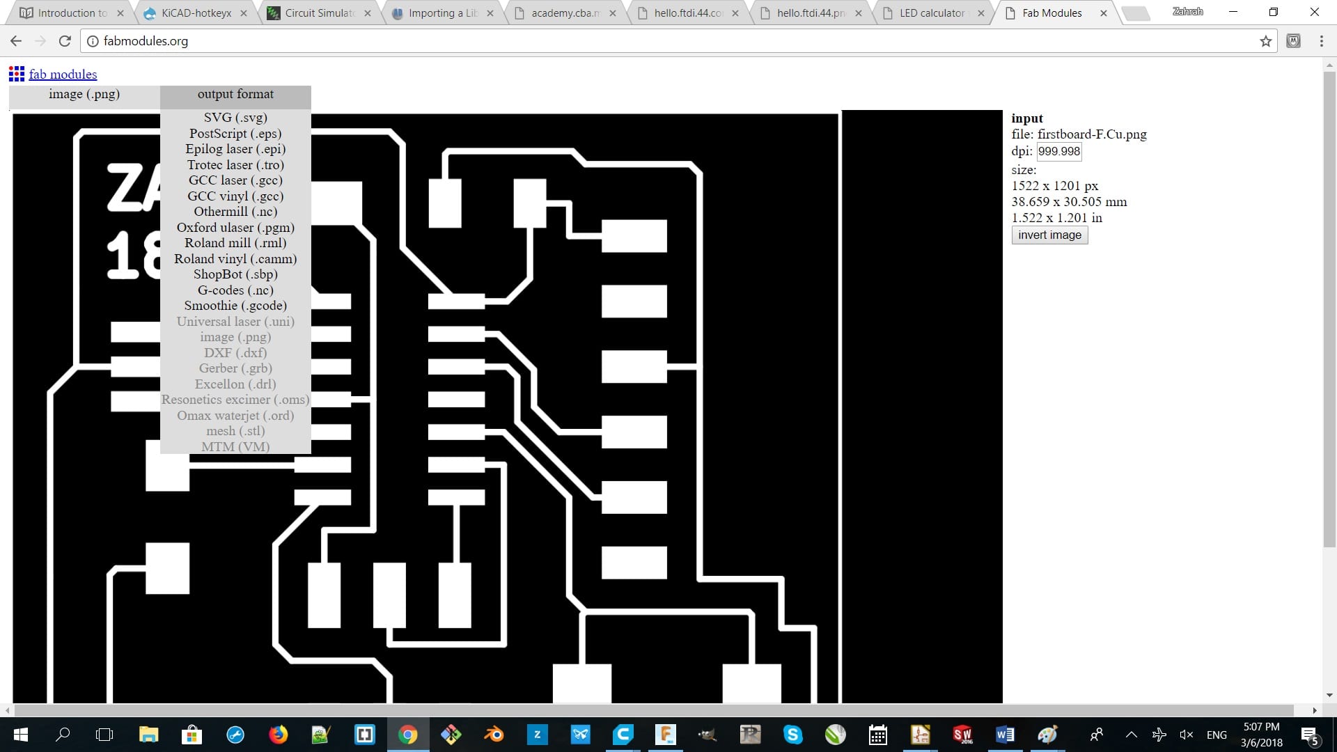
3. PCB traces (1/64) and this is the size of mill bit for the cutting the traces
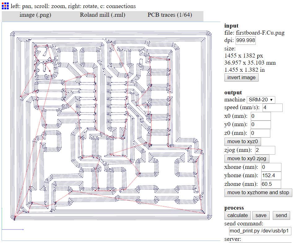
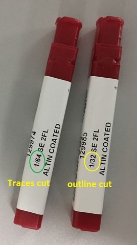
Well, because of choosing the wrong mill bit I chose the 1/32 mill bit instead of 1/64 and to be honest it is interesting that the mill bit didn’t break and I liked how the board looked that the reflection of the light comes through and I did another new one of course :)
which I suppose to choose the 1/64 for tracing the circuit.
But tbh the result of that is interesting :) .. the mill bit is really strong and did not broke!!
honestly, I liked how the board looks like with the trace 1/32 :) I can imagine the reflection of light through this circuit board ..
See the video of that.
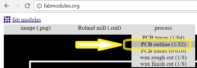
again, here is the second milling of the circuit board with the correct process "trace and correct mill bit 1/64"
sometimes when I work I forget to take pictures for documenting my work!! unfortunately, I didn't take any picture of my work while I'm soldering the components and testing the board connections.
So in week 5 you will remember that I described these procedures Electronic production's Week 5 this is another good chance to improve my skills in making boards, soldering and of course adding to my basic knowledge about the circuit board components.
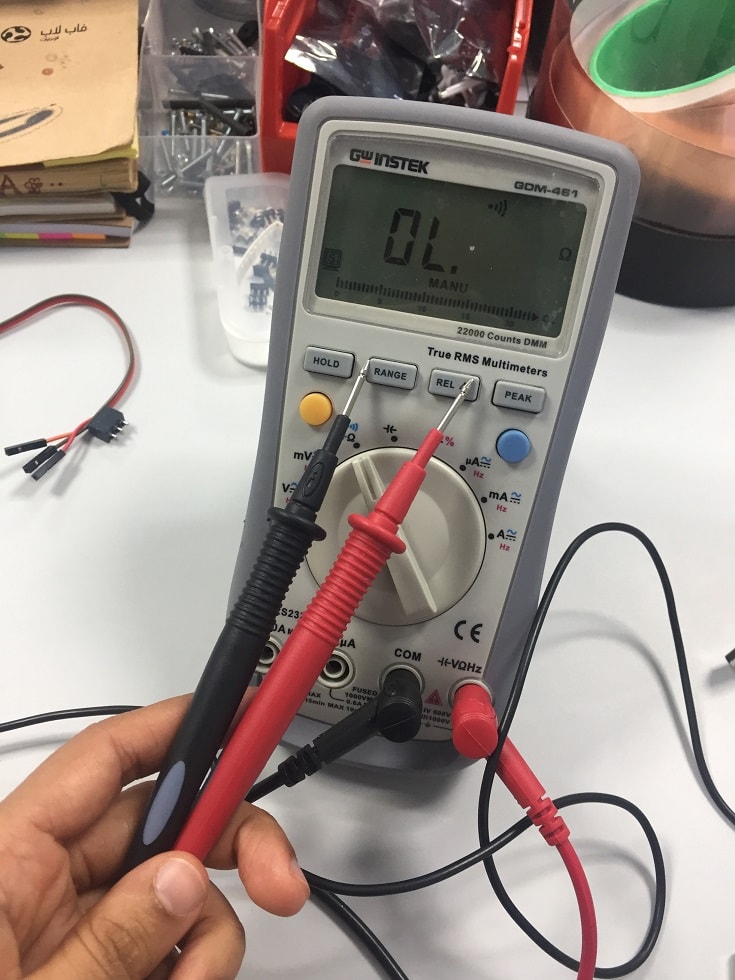
For testing the efficiency of soldering and component's connection I used a millimeter to test the connections using the continuity  function where the dial pointing and you can see it on the screen.
So, the millimeter has two cables Red and Black. If there is a sound while you pointing both cables in same route or line this is an indicator for connections in this line.
this is how I tested my board traces and components connection.
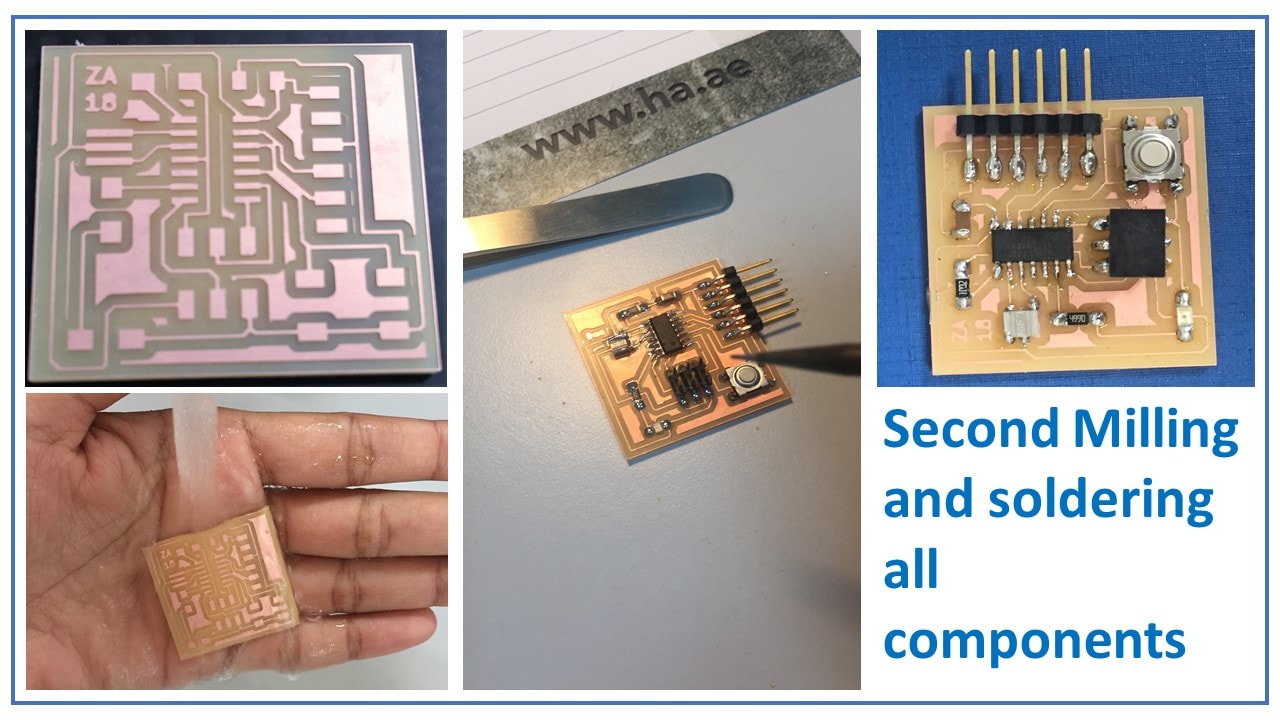
Here I want to point out my soldering and how it improves from the first time I did solder as it was first time in my life to do soldering !! see this board and the fab ISP board I did In week Electronic production's Week 5 .
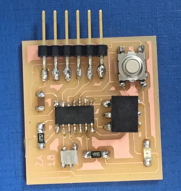
This is everything I did this week and for testing the board I did use the oscilloscope in week project development to check the board and in Embedded Programming Week 9 you check on how we programed this board.