
Our local instructor this week was Juha-Pekka Mäkelä. This week we need to measure something. For that, we need to create a board with a sensor, and get the values from it. This week I will definitely need to go back to assignment 7 (electronics design) and assignment 9 (embedded programming).
I want to do some sensors I could use for the final project. I have decided to use a hall-effect sensor, to detect if the doors of the wardrobe are open or closed. I want to separate the micro from the sensors, so I will design two different boards.
To Do
- Design the boards
- Mill the boards and solder
- Program the boards
- Group work
The "Doing"
Design the boards
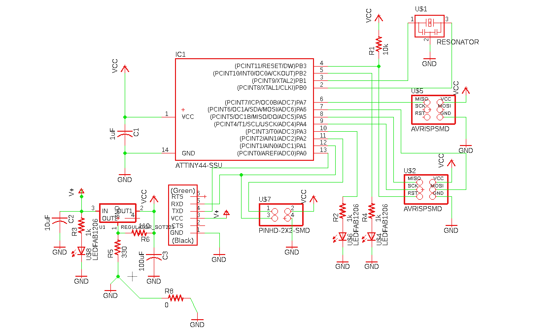
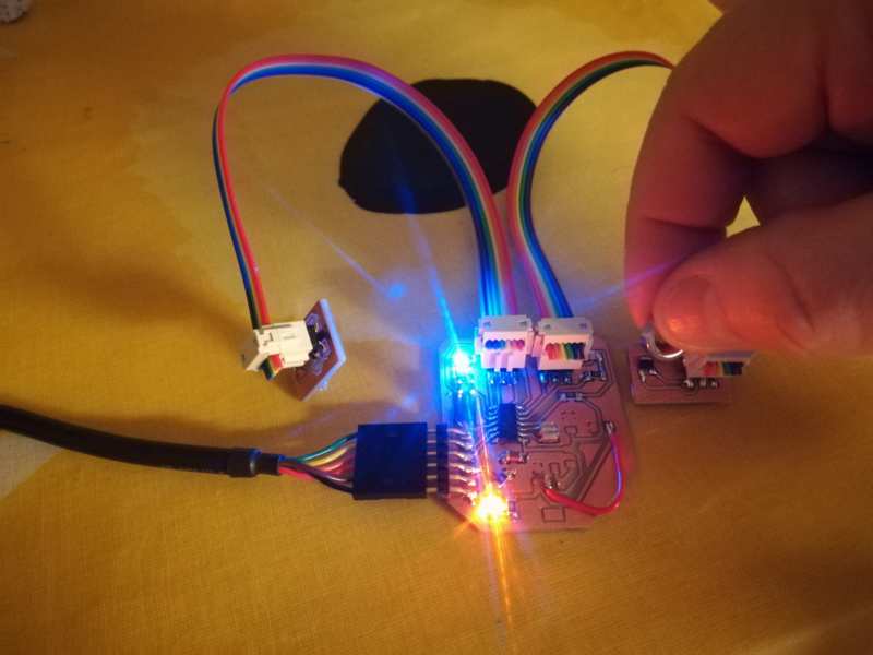
- One board for the ATtiny44 (Main Board) and one for each sensor (Sensor Board)
- The Main board needs:
- FTDI connector
- 3x2 Pin header for programming the micro
- Some connector for connecting the sensors
- I want two Hall-effect sensors: I will reuse the programming header pin for one of them
- I decided to add another 3x2 pin header for the other hall-effect sensor (two much, but like this it looks the same)
- 2x2 pin header for future communication
- Leds for feedback> one per sensor
- Resonator
- Voltage regulator (ZLDO1117 data sheet), because I want to feed my board with a battery
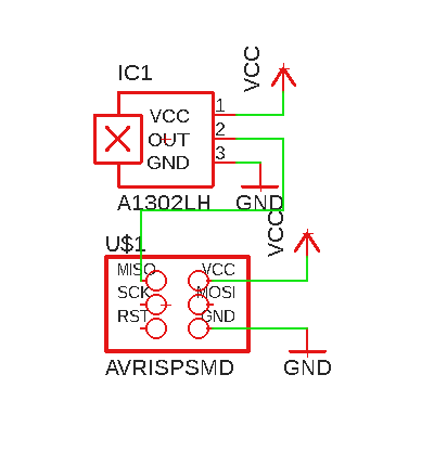
- Sensor board needs (according to the data sheet):
- 3x2 pin header and sensor
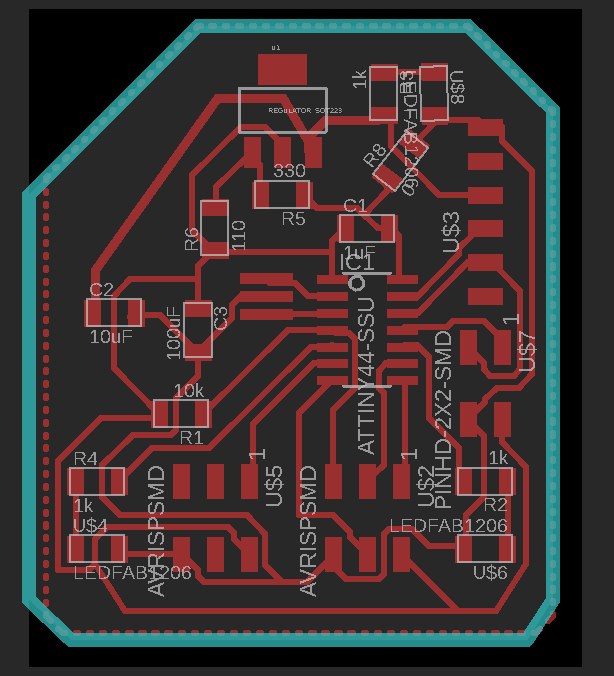
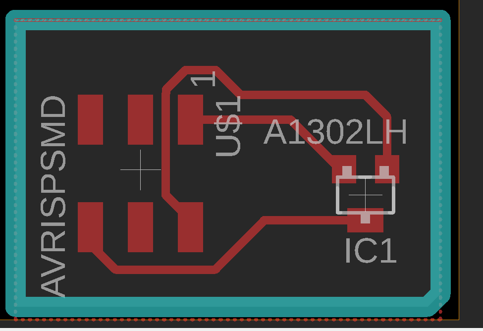
Mill the boards and solder
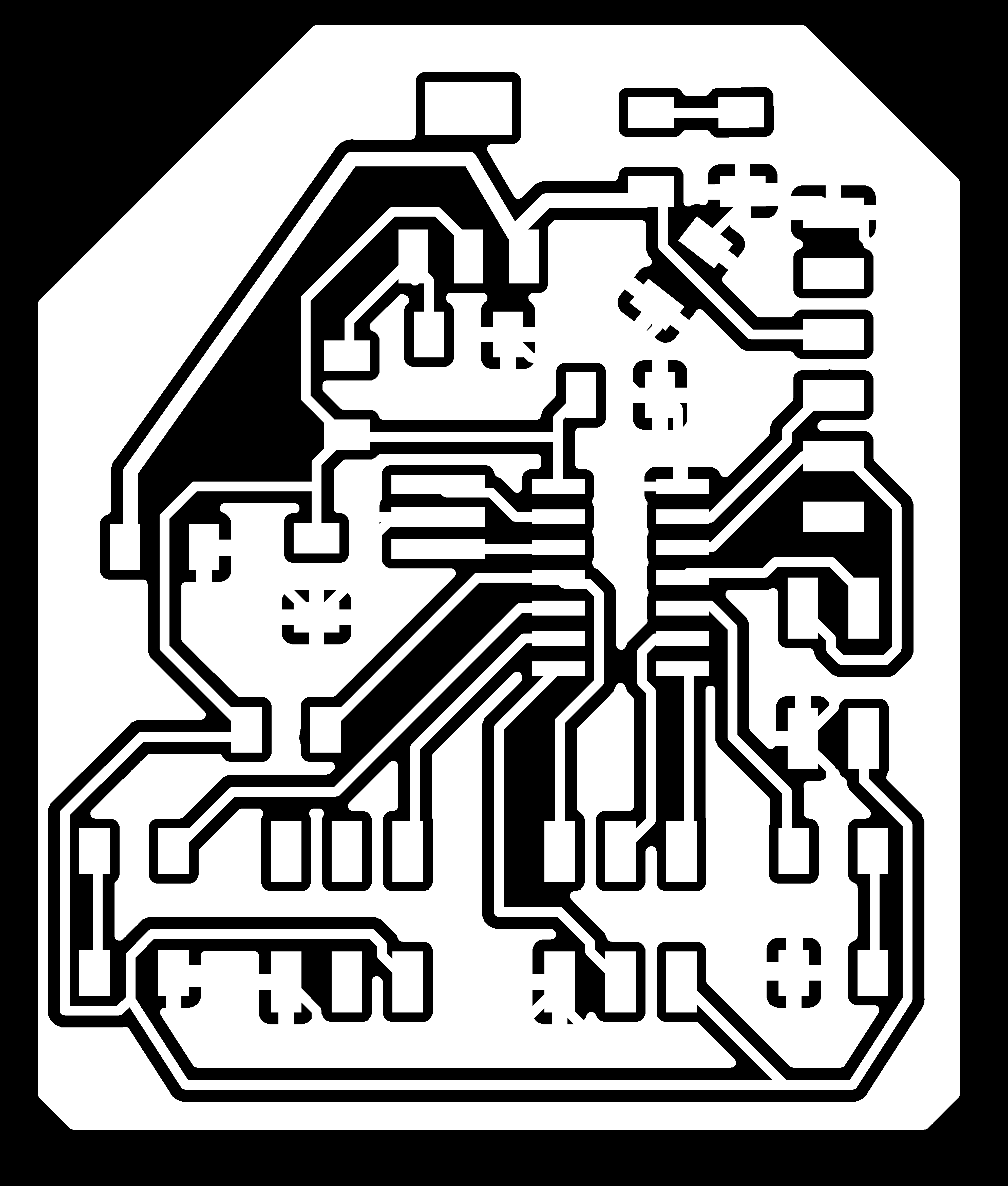
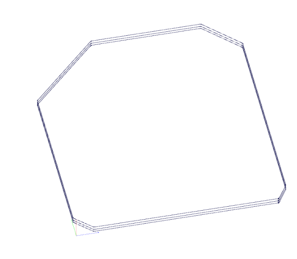
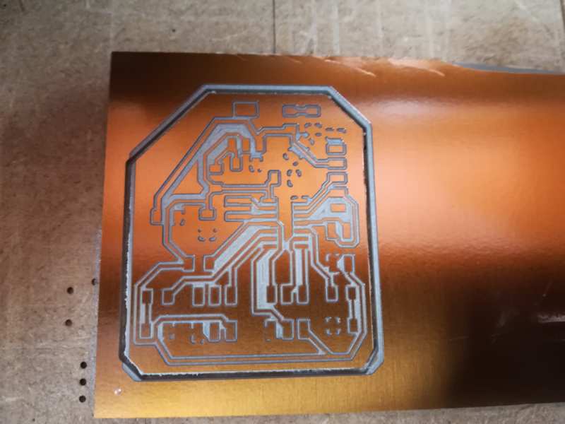
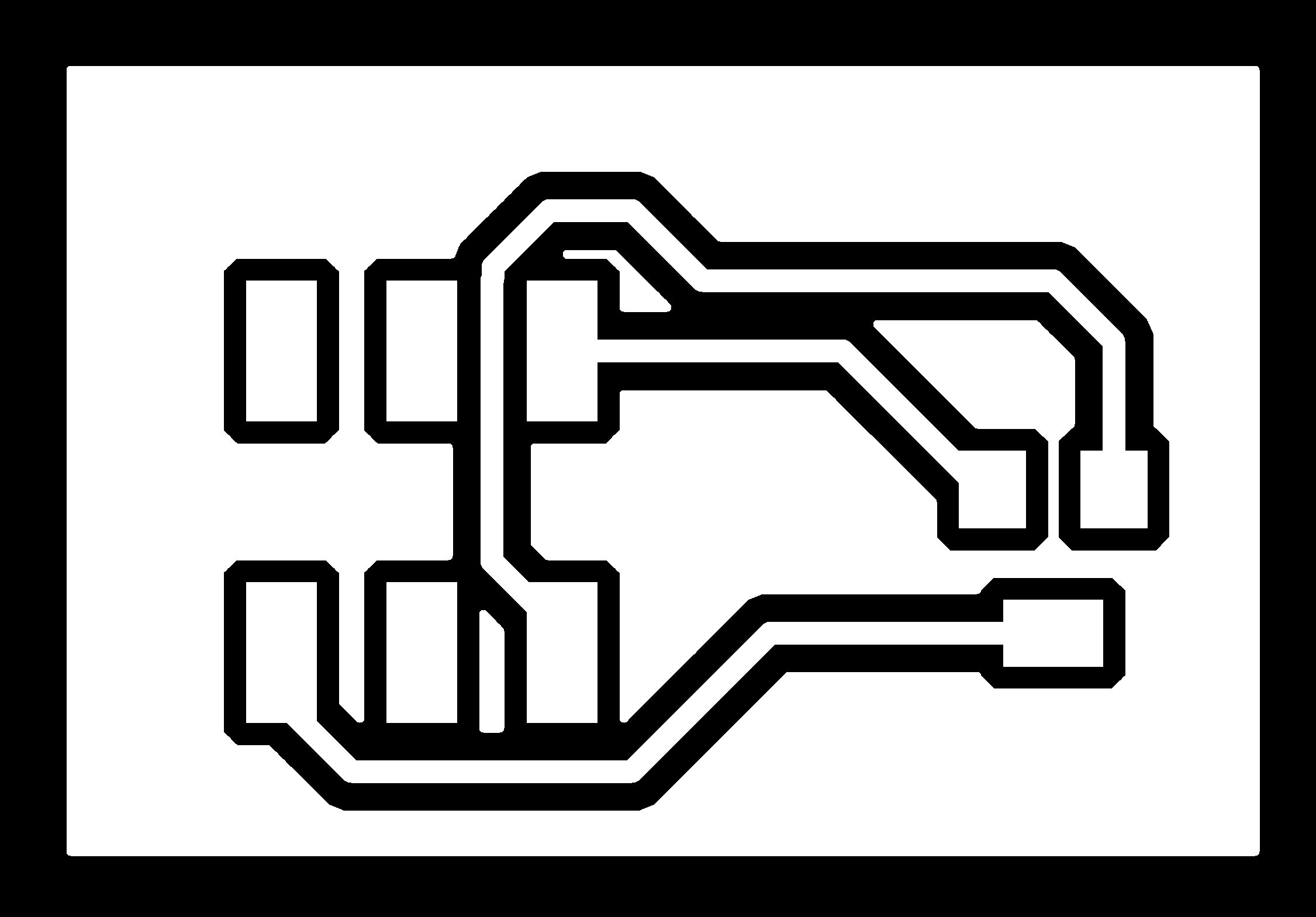
- Get the outline and traces images
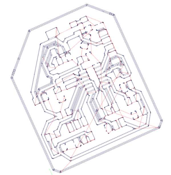
- Get the toolpaths for outline and traces (in the pictures just for the main board)
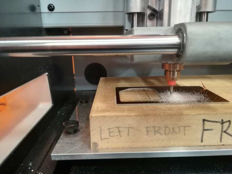
- Mill


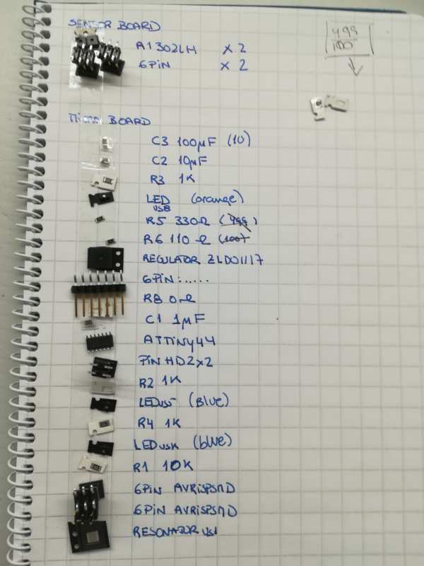
 Bill of materials
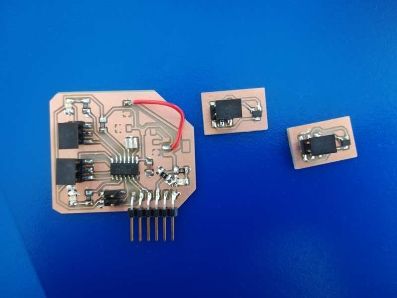
- NOTE: I ended up not soldering yet the voltage regulator(That is the reason for the jumper). Probably it wont work with the FTDI cable. Once I have programed and tested, I will come back to this.
- NOTE: the Basic Adjustable Regulator with 5V Output specified in its data sheet circuit may not be needed.
Program the boards
- What? I want to turn off a LED when the sensor detects the magnet
- How?
- I decided I will first try the Digital reading, in order to fulfill the assignment.
- And then, with that working, I would try the Analog Reading too.
Digital reading
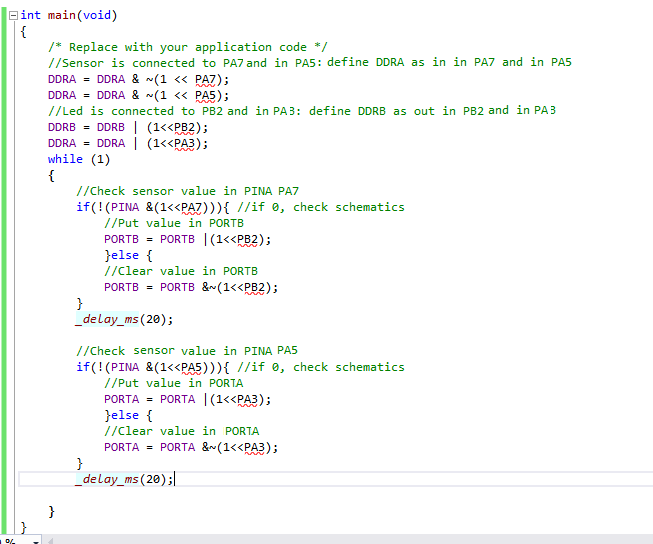
I will start with digital. To test if it is working, I think it will be enough. Each magnet switches off one LED when it gets close to the corresponding sensor.
I will use a code quite similar to the one for the switch on assignment 09 (switch value read from PA5), but taking into account nowI need to read two IN pins (PA7 and PA5) and write into two OUT pins (PB2 and PA3).
Analog reading: extra
Again, I have two Hall-Effect sensors and two LEDs. I want to switch off the corresponding LED when the magnet is just close to the sensor. That way it will be with the doors in the final projects.
START FROM DATASHEET
It 's time to go back to the ATtiny datasheet to check how the analog to digital converter works. This is a summary:
- ATtiny44A features a 10-bit, successive approximation Analog-to-Digital Converter (ADC)
- The ADC is enabled by setting the ADC Enable bit, ADEN in ADCSRA
- The ADC does not consume power when ADEN is cleared
- ADC converts an analog input voltage to a 10-bit digital value
- min value = GND; max value = Voltage reference
- Voltage reference
- selected by writing the REFS[1:0] bits in the ADMUX register
- Alternatives are the VCC supply pin, the AREF pin and the internal 1.1V voltage reference
- The analog input channel and differential gain are selected by writing to the MUX bits in ADMUX
- Any of the ADC input pins can be selected as single ended inputs to the ADC
- The ADC generates a 10-bit result which is presented in the ADC Data Registers, ADCH and ADCL
- By default, the result is presented right adjusted
- can optionally be presented left adjusted by setting the ADLAR bit in ADCSRB.
- If the result is left adjusted and no more than 8-bit precision is required, it is sufficient to read ADCH, only.
- Otherwise, ADCL must be read first, then ADCH, to ensure that the content of the data registers belongs to the same conversion.
- Once ADCL is read, ADC access to data registers is blocked.
- This means that if ADCL has been read, and a conversion completes before ADCH is read, neither register is updated and the result from the conversion is lost.
- When ADCH is read, ADC access to the ADCH and ADCL Registers is re-enabled
- Make sure the ADC is powered by clearing the ADC Power Reduction bit, PRADC, in the Power Reduction Register, PRR
- A single conversion is started by writing a logical one to the ADC Start Conversion bit, ADSC
- bit stays high as long as the conversion is in progress and will be cleared by hardware when the conversion is completed
- If a different data channel is selected while a conversion is in progress, the ADC will finish the current conversion before performing the channel change
- Alternatively, a conversion can be triggered automatically by various sources
- Auto Triggering is enabled by setting the ADC Auto Trigger Enable bit, ADATE in ADCSRA
- (check more if needed)
- the successive approximation circuitry requires an input clock frequency between 50kHz and 200kHz to get maximum resolution
- The prescaling is set by the ADPS bits in ADCSRA
- The prescaler starts counting from the moment the ADC is switched on by setting the ADEN bit in ADCSRA
- The MUX[5:0] and REFS[1:0] bits in the ADMUX Register are single buffered through a temporary register to which the CPU has random access
- The channel and reference selection is continuously updated until a conversion is started. Once the conversion starts, the channel and reference selection is locked to ensure a sufficient sampling time for the ADC. Continuous updating resumes in the last ADC clock cycle before the conversion completes (ADIF in ADCSRA is set). Note that the conversion starts on the following rising ADC clock edge after ADSC is written. The user is thus advised not to write new channel or reference selection values to ADMUX until one ADC clock cycle after ADSC is written.
- ADMUX can be safely updated in the following ways:
- When ADATE or ADEN is cleared.
- During conversion, minimum one ADC clock cycle after the trigger event.
- After a conversion, before the Interrupt Flag used as trigger source is cleared.
- When updating ADMUX in one of these conditions, the new settings will affect the next ADC conversion.
- In Single Conversion mode, always select the channel before starting the conversion. The channel selection may be changed one ADC clock cycle after writing one to ADSC. However,the simplest method is to wait for the conversion to complete before changing the channel selection
- ADMUX
- Bits 7:6 – REFS[1:0]: Reference Selection Bits
- Voltage Reference to VCC => REFS1=0 and REFS0=0
- Bits 5:0 – MUX[5:0]: Analog Channel and Gain Selection Bits
- Interesting values on Table 16.4: define the PIN you get data from
- Bits 7:6 – REFS[1:0]: Reference Selection Bits
From the summary above, I need for programming:
- You can read just from one analog input at a time
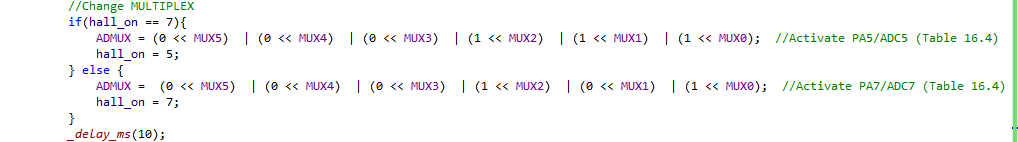
- With ADMUX you can define from where you read: I need to change it in every loop, so I can read from both sensors
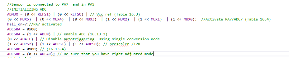
- I have the two HAllEffect sensors to PA5 and PA7. Checking from the table 16.4, I know the first bits of the ADMUX should be 000111 for PA7 and 000101 for PA5
- We want the Voltage Reference to VCC, so last bits of ADMUX to 00
- You need to enable ADC: set ADEN in ADCSRA
- We need to adapt the frequency, with the prescaler
- Set ADLAR bit to get left presented data
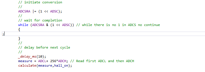
- Then, remember to read first the low register and then the high register
 Changing the analog input
 Wait for the data and read it the data
 UPDATE FROM WEEK 13: In the actual board of this assignment, I just switch on/off the corresponding LED of each Hall Effect sensor when the magnet is close/far. But for the Interface assignment I sent the analog values and visualize those values showing the progress of the proximity of the magnet to one of the sensors.
Resources
- ATtiny44a data sheet
- HallEffect sensors and magnets
- HAll-Effect sensor data sheet
- Voltage regulator data sheet
- AtmelStudio
Once done
Summary
- I have designed a board for my microcontroller
- I have designed a board for a hall-effect sensor
- I have milled both of them
- I have programmed the ATtiny44A to get digital data from the HAll Effect sensors and actuate over two different LEDs
- I have programmed the ATtiny44A to get analog data from the HAll effect sensors and actuate over two different LEDs
Difficulties
- Time, time, time...
- I still have issues soldering the resonator... But getting better
- Get data from the analog inputs. Although finally it was not that difficult. It was just about the time required to read the datasheet to understand what was needed
Learnings
- I thought to separate the voltage regulator to another board. Maybe I should have done that, because sometimes, modularity helps for debugging!
Tips
- Remember, when using this in the Final Project, to put the magnets in the correct position as the magnetic field values depend on the magnetic side
Files
- main.c C file for switching on/off light from two hall effect sensors connected to a board
- Eagle board file and Eagle schematic file for the board: microcontroller
- Outline for the board: microcontroller
- Traces for the board: microcontroller
- Eagle board file and Eagle schematic file for the board:sensor
- Outline for the board:sensor
- Traces for the board:sensor