Electronics Design
Table of contents
Schematic Entry
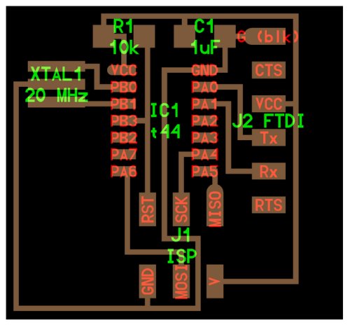
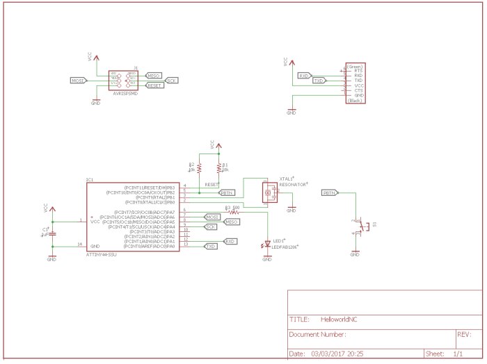
The design process for most electronic circuit boards begins with a schematic which indicates in symbolic form the main electronic components and how they are connected together. This forms the basis for the printed circuit board (pcb) design: the physical representaton of the circuit. The original HelloWorld board did not have a schematic so using the original circuit layout and parts list a schematic was drawn up using Eagle PCB design software.
To begin designing a schematic the various parts that are required must either be already avaialable in the Eagle CAD format or the designer needs to create them in that format. These parts will have a symbolic representation which will indicate the part functionality: a resistor, capacitor, switch or integrated circuit, etc. They will also have an actual size and shape which will contain the various dimensions and structure of the electrical connections. This part information, symbolic and physical is stored within a parts library.
Fortunately for the HelloWorld board a parts library already exists in the Eagle format. This can be downloaded from http://fab.cba.mit.edu/classes/863.16/doc/tutorials/electronics/ The library should be saved in the Eagle Library folder which typically can be found on the local drive at C:\EAGLE-7.6.0\lbr
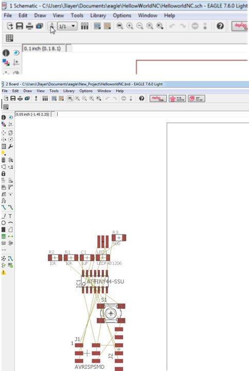
Once the library had been downloaded the Eagle software was started and opened in Control Panel.
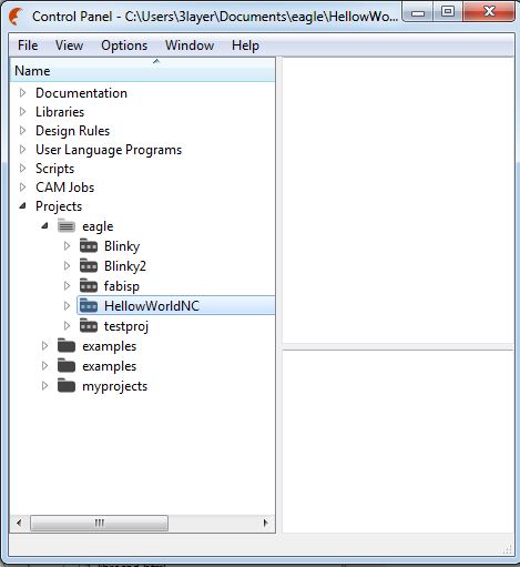
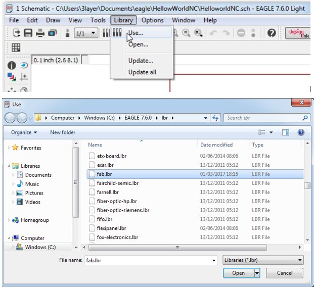
Right clicking on the Eagle folder within the Control Panel Projects tab allowed me to create a new project called HelloWorldNC. Right clicking on the newly created project brought up a menu which allowed a new schematic to be created. Before any parts from the Fab Lab library can be added Eagle needs to be told to 'use' that particular library. This was accomplished by going to the library menu, selecting use and then browsing to where fab.lbr was stored and 'using' it.
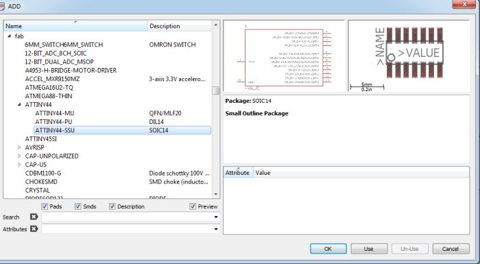
With the library in use I was then able to add the required parts to the schematic. The parts added were as follows with the link to the bill of materials provided at the end of this article. Note that some of the components such as resistors and capacitors are initially added from the Eagle Parts Library as generic parts, for example a 1206 resistor. For these type of parts it is up to the designer to add the component value information so that the schematic is a true representation of the specified circuit.
- 1 x ATTINY44-SSU
- 1 x FTDI-SMD-HEADER
- 1 x CAP-UNPOLARIZEDFAB
- 1 x LEDFAB1206
- 1 x AVRISPSMD
- 1 x 6MM_SWITCH6MM_SWITCH
- 3 x RES-US1206FAB
With the parts added the various connections were made and the schematic entry of the circuit design completed.
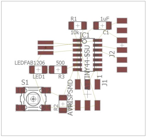
With the schematic completed the next step was to move to pcb design. From the Eagle schematic tool bar the switch to board button was selected. This created a pcb and placed the components outside the board
Printed circuit board design
Design Rules
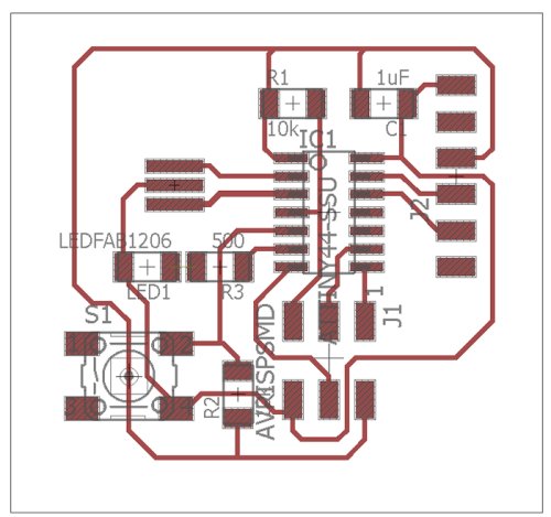
The pcb parts are placed on the board and the electrical connections routed to them. Before this can happen the design rules for how that particular board will be laid out need entered into the CAD software. The design rules ensure the printed circuit board can be made and take into account the manufacturing process, which in this case is isolation routing using the Modela MDX-20 and a 1/64 inch end mill. Given the end mill diameter of approximately 16 mil this will determine the minimum route seperation between adjacent traces and component pads.
The trace width needs to be decided also : too wide and the board will be difficult to route, too narrow and the milling process may lift traces. Previous board designs that were manufactured using the MDX-20 used a trace width of 12 mil so this value was chosen for the HelloWordNC board.
| Design Rules | Parameter | |
|---|---|---|
| trace to trace | 16 mil | |
| trace to pad | 16 mil | |
| trace to via | 16 mil | |
| pad to pad | 16 mil | |
| min trace width | 12 mil |
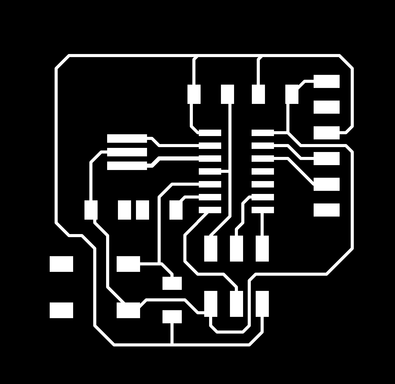
Layout
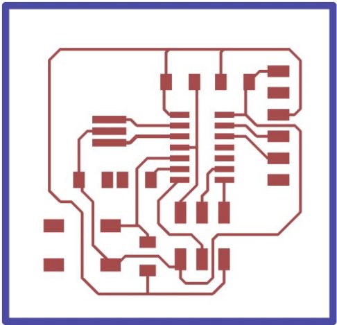
The pcb components were moved onto the board and placed in positions to make routing easier. When components are initially placed, Eagle shows light coloured lines between component pads that are connected on the schematic and should be connected in the pcb layout. These lines help when placing the components as they indicate where best to place a part to help with routing. Once the components were placed the pcb was laid out on the top pcb layer. In order to cut out the board a second layer is needed that contains the shape and dimensions of the cutout. This cutout information was drawn on the bottom layer, although it could have been drawn on any layer. Prior to generating the manufacturing files a design rules check (DRC) was performd on the board by selecting Tools->DRC->Check from the pcb layout menu
PCB outline
The pcb design needs to include a board outline that will be used to cut and shape the pcb to the correct dimensions. To create a board outline, select the line tool in Eagle. Change the line width to a value greater than the diameter of routing bit that will be used by the Modela MDX-20 to cut out the pcb. In this case the line width was set to 0.032". Select the layer the line is to be drawn on and then draw an outline shape around the pcb. In this case the bottom layer was used to draw a rectangle outline around the top layer electrical connections - shown blue in the final image.
Preparing the manufacturing files
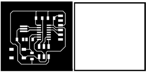
The Fab modules require monochrome png files in order to generate the milling paths for the MDX-20. For this project two png files are needed:
- The routed layout
- The board outline
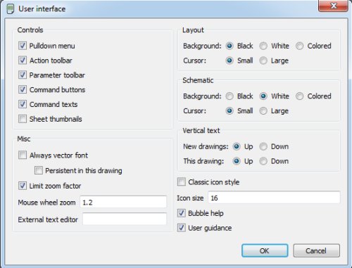
These files can be produced in Eagle when in the PCB layout tool, by selecting Layer Settings and only making visible the routing layer for which the png is to be generated. For the pcb taces this meant having only the top layer visible and for the cutout png the bottom layer was the only one visible. Another point regarding the pcb trace layer, was that to generate the image file so that the traces appeared white on a black background the background in Eagle pcb layout tool had to be changed to black. This is achieved by going to the Menu and selecting Options->User Interface and changing the settings. Note for the cutout layer the background colour was not changed have to happen.
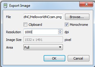
The png files are generated by Menu->File-Export->Image and setting the parameter for the png file, which need to be monochrome and 1000 dpi - not sure about this last setting
Manufacturing
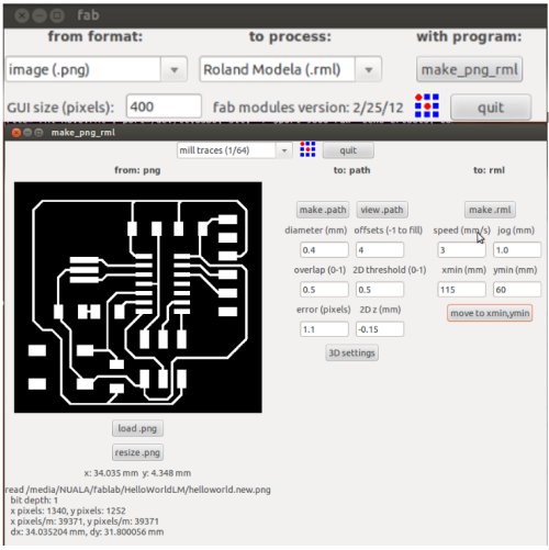
The png routing file was loaded into Fab Modules using the setup shown below:. The make path function was called and this created the toolpath
for the Modela MDX-20 to route the board out.
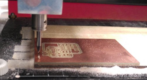
The finished board is shown below. There was a problem with the cutout because it appears offset with respect to the pcb traces by about 10mm. I did not notice this until the board was being cut out. As it was too late to route another board I stopped the Modela and cut the board out manually with a guillotine - which wasn't a great idea as the FR1 material is brittle when compared to FR4 and the pcb started to crack. You can notice this in the photograph.
I think the offset was caused when I was demonstrating Eagle to someone and put an extra resistor on the schematic. This would have appeared on the board but outside the board outline and because I was looking at the bottom layer for the outline, the resistor would not have appeared but may have caused the png to introduce an offset. This is only a theory and needs verified or falsified.
Another issue with the cutout is that originally the Fab modules would not create a path for it. I think this was caused by the width of the cutout trace being narrower than the 1/32nd routing bit. I increased the cutout width to 32mil and loaded the new png into Fab Modules and the path was created.

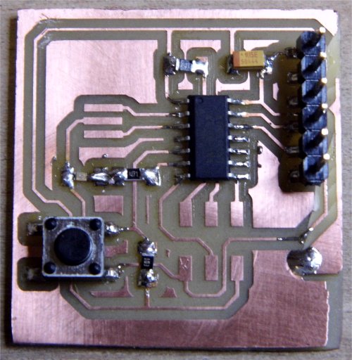
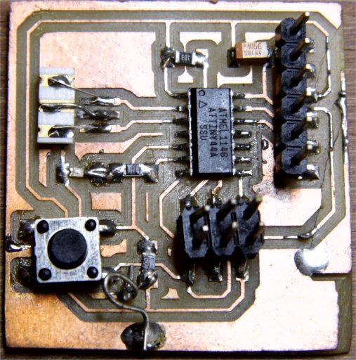
We did not have all the components in the FabLab so I used whatever suitable parts I had to assemble the HelloworldNC board. Some of these components are 0805 size and they were just about able to span the pad width of the 1206 footprint. Likewise the resonator was the wrong footprint so I had to add wire links from resonator pads to pcb.
The photos below show the final board assembly. The board can be shown working in the embedded programming assignment here.
Downloads
The various files for producing the HelloWorldNC board are available here along with a bill of materials.