Networking and Communications
Table of contents
Introduction
The nRF24L01+ is a 2.4GHz radio transceiver chip from Nordic Semiconductor. Various low cost modules using this IC are available which, when coupled with control
electronics and software facilitate the easy implementation of a radio link for networking and communications. For this assignment I decided to use the nRF24L01+ modules
to create a radio communications link between two processors. Most of the information describing how to use these moudles is available from
www.arduino-info.wikispaces.com/Nrf24L01-2.4GHz-HowTo
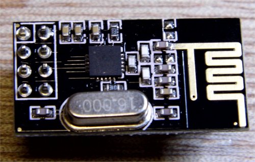
The nRF24L01+ uses a proprietary packet protocol called Enhanced ShockBurst to send and receive data over RF. For a bi-directional link each module can operate as a transmitter or receiver. When operating as a transmitter data sent to the nRF24L01+ is packetized according to the protocol and then transmitted. When configured as a receiver the Nrf24l01+ constantly searches the received data for a valid address and if detected will then process the incoming data. Control of the module is effected over SPI and various configuration parameters such as data rate and output power can be set up over SPI. An Arduino library for the nRF24L01+ has been developed to simplify developing with this device. This comes with example sketches and I decided to use the GettingStarted sketch as the code part of this assignment.
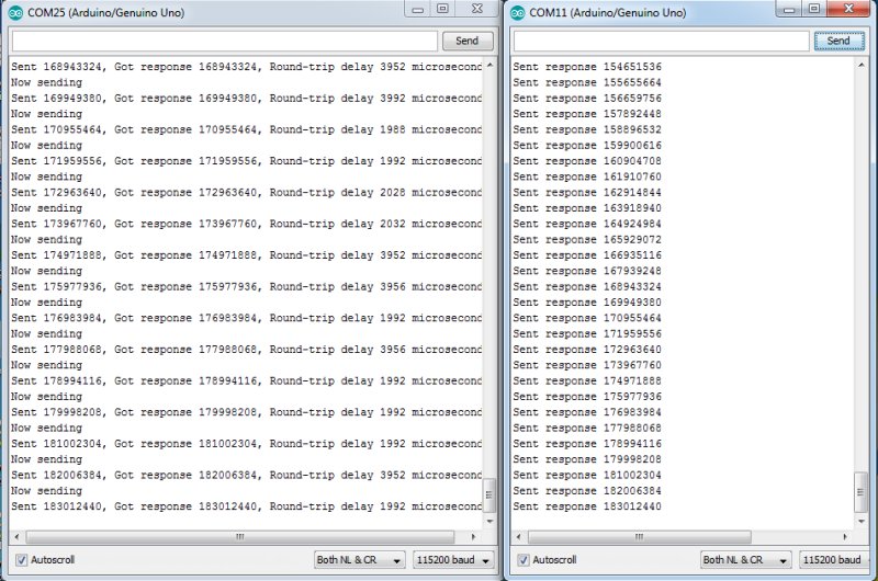
This sketch configures the nRF24L01+ modules with addresses (0,1) and using the Arduino serial monitor allows the user to initially configure one of the modules as the master transmitter This transmits the time in microseconds to the other module using its address. The other module then replies with the received time packet and the master module prints this in the serial monitor along with the round trip time. If the master module doesn't connect the RF link, then it will signal this in the serial monitor window.
Initial tests
Before desiging any electronics I tested the modules could be controlled by Arduino. An Arduino library for the nRF2401 with examples can be downloaded from https://github.com/nRF24/RF24/tree/master/examples. I uploaded the GettingStarted sketch and connected the Arduino to the nRF24L01+ modules according to the table below.
| nRF24L01+ pin | Arduino pin | Signal name |
|---|---|---|
| 1 | GND | gnd |
| 3 | 7 | CE |
| 4 | 8 | CSN |
| 5 | 13 | SCK |
| 6 | 11 | MOSI |
| 7 | 12 | MISO |
Pin 2 of the nRF24L01+ module is the VCC supply which is 3.3V. This wasn't connected to the 3.3V of the Arduino because there is concern that the modules draw too much power from the Arduino and will not work. For the module's VCC supply I created a seperate 3.3V supply on some prototyping board and connected this to the module.
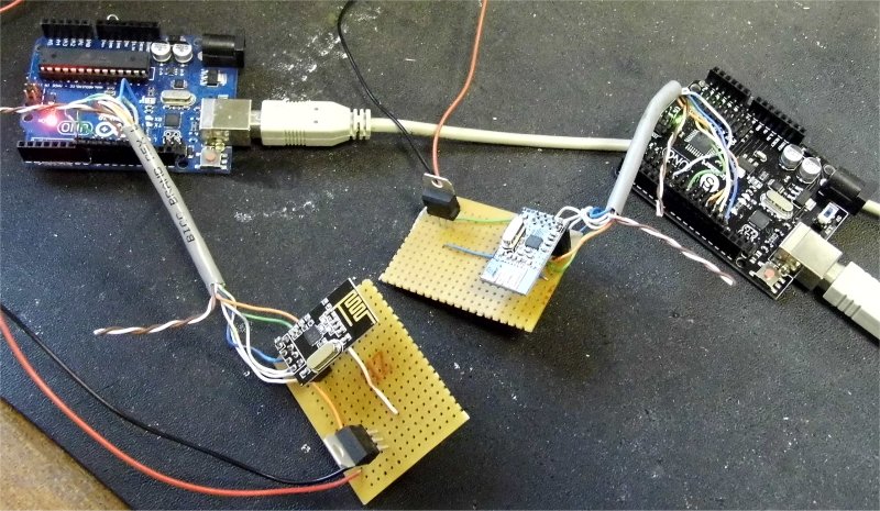 The two modules were connected to two different Arduino's and the GettingStarted sketch uploaded to each Arduino in turn. The steps to do this are listed below.
- Wire the Arduinos to the modules according to the wiring diagram above.
- Plug each Arduino into a computer USB port and note the com port number associated with each Arduino.
- Power the modules if not powered already from the Arduino board.
- Open Arduino IDE and load GettingStarted sketch - will come with the RF24 library.
- Note Arduino and associated com port and upload sketch.
- Open serial monitor in Arduino IDE and change serial port settings to 115200 baud - you will be prompted to press 'T' for transmit - if not code is not running.
- Open a second version of Arduino IDE and load the GettingStarted sketch - change the code from bool radioNumber = 0 to bool radioNumber = 1
- Upload the code for the second Arduino.
- In the serial monitor for the first Arduino enter T to tranmit the synchronising message.
After following these steps the serial monitor for the transmit Arduino repsonded with an error message
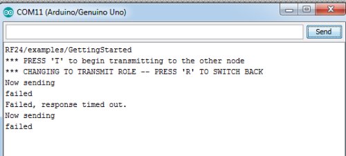
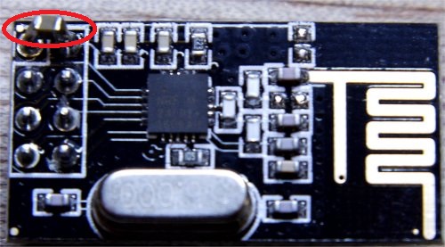
After re-checking the connections I noticed that www.arduino-info.wikispaces.com/Nrf24L01-2.4GHz-HowTo suggested adding a capacitor to the nRF24L01+ power supply pins so I soldered a 10uF 0805 capacitor across pins 1 and 2 of the nRF24L01+ module.
I reconnected the modules to the Arduino and powered everything up. I opened up the serial monitor for both Trasnmitter and Receiver Arduinos and noted the communications link was working.
Hardware
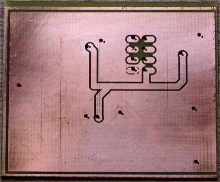
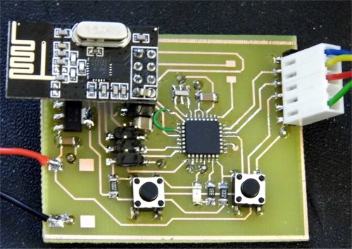
For the electronics I decided to design an Arduino type board that would control the nRF24L01+. This would allow me to develop code using the Arduino IDE and give me some experience in using a different processor and also help towards designing the processor board for my final project. I chose the ATMEGA328P and created a schematic containing this processor, a UART link, a 3V3 regulated power supply and a connector to plug in the nRF24L01+.
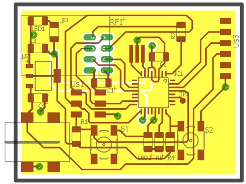
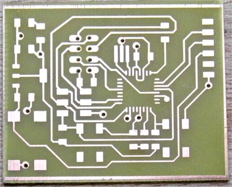
Because I couldn't get to the local Fab Lab in Derry and use the Modela MDX-20, I etched the board using photo resist FR4. I printed the Eagle pcb layout onto Laserstar semi-transparent paper and then placed this artwork over photo resist FR4 and exposed this for 3 minutes under a UV light source. I then developed the board using sodium hydroxide to remove the unwanted photo resist and then placed the board into a ferric chloride etching tank which removed all the exposed copper leaving the required connections.
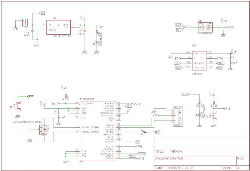
The board is double sided with the bottom layer containing the ground layer and VCC routing.
Assembly and testing
The components were assembled onto the pcb and when complete the USBTiny programmer was connected to it and powered on. Arduino IDE was opened and under the tools menu, making sure the Board was Arduino/Genuino Uno, Burn Bootloader was selected. This programmes the bootloader code into the ATMEGA328P and uses the external 16MHz crystal/resonator. I got an error indicating the device signature was incorrect.
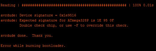
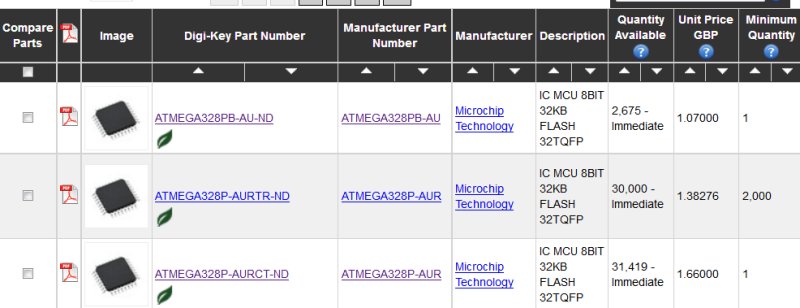
With further investigation I found out I had ordered the incorrect IC, the ATMEGA328PB instead of the ATMEGA328P.
This has the device signature of 0x1e9516. Following recommendations on an Arduino web page I opened the Arduino configuration file, avrdude.conf, in a text editor. On my PC this lives in C:\Program Files (x86)\Arduino\hardware\tools\avr\etc. I modified the signature to 0x1e 0x95 0x16. Saved the file, opened Arduino IDE and ran the Burn Bootloader command. This time it was successful.

I plugged in my FTDI cable which I had bought/made for a previous assignment into the pcbs UART header. A new Arduino sketch was created which would blink LED2 on the board. In the Arduino Tools menu, the correct com port for the FTDI cable was selected - followed by the Upload command. The console showed that Arduino IDE couldn't connect to the board. The connections were rechecked and the internet Googled as for a reason. Some web pages suggested that the ATMEGA328PB had UART issues within Arduino IDE, so I disoldered this part from the board and soldered in place an old ATMEGA328 that I had. Going through the same procedure as before the avrdude.conf file had to be modified with the ATMEGA328 signature of 0x1e 0x95 0x14 and the Burn Bootloader process run through. Again there was no success with uploading the code over the com port. The USBTiny programming lead was plugged in and this time from the Sketch menu the command Upload using Programmer was selected. Success - LED2 blinked.
RF link
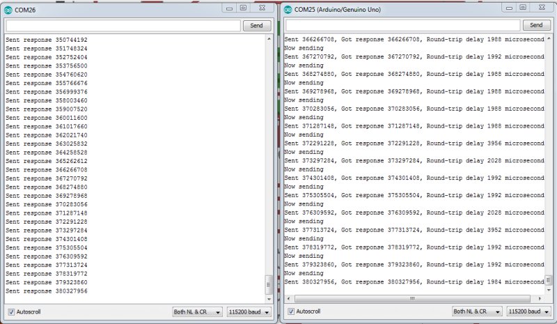
Due to all the time spent debugging I only had one board assembled with the ATMEGA328 and the nRF24L01+ module so I decided to create the RF link using my board and an existing Arduino UNO. The GettingStarted sketch was loaded and the steps described in the Initial Tests section ran through. The Arduino Uno was configured as radioNumber 1 and the ATMEGA328 board as radioNumber 0. The code was uploaded to each board in turn and the serial monitor opened. The Arduino Uno was configured for transmit but the response in the serial monitor indicated there was no response from the other board.
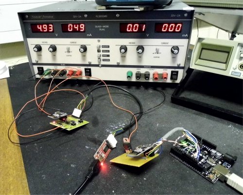
Rechecking the connections on the ATMEGA328 board I found the nRF24L01+ CE pin was going to the wrong pin on the ATMEGA328. It was going to PC5 instead of PD7. I made a small wire link and connected PD7 to the pcb trace going to the CE pin of the RF module.
After connecting up the correct pin, Arduino IDE and serial monitor was opened for both boards. The Arduino Uno board was configured to transmit and this time the link worked.
Downloads
- Eagle design files
- PNG layout files
- LED2 Blink sketch
- Eagle library containing additional parts.
- nRF24 Arduino library and examples.