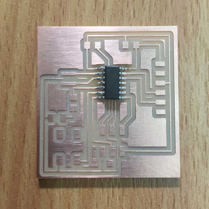
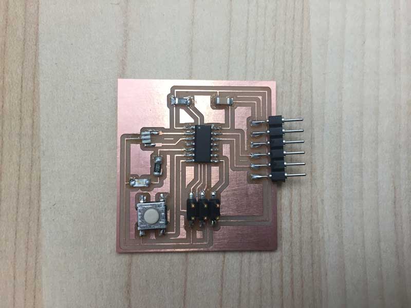
Electronics Design
Design Files
- Eagle File for my Hello World Board
- Eagle File for my Hello World Schematic
- Hello World Board Edited in Adobe Illustrator
Group Assignment
Designing a circuit board with LED and button, using Autodesk Eagle.
Schematic Design
This week involved learning a new software, Autodesk Eagle. It was daunting at first, because the user interface is not as user friendly as the other Autodesk software I've used. It's not obvious where to start, so I watched the following video guide:
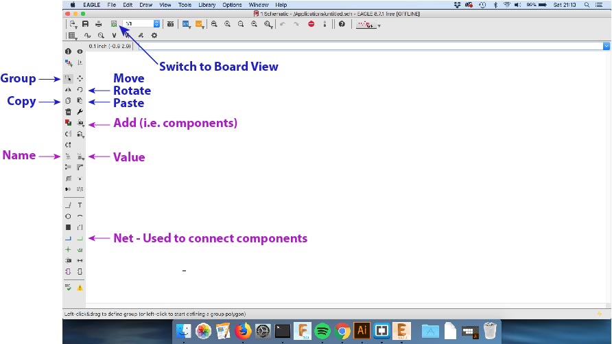
Once you open the software go to File > New > Schematic. It's not obvious where to start, so I've created a visual guide to the tools I used.
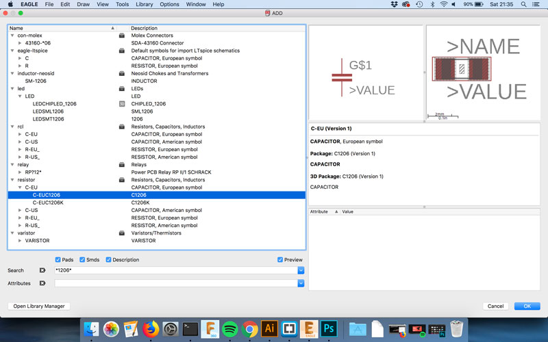
Click on Add to find components from the built in libraries, as shown below. It took me a while to find out that the search bar will only search for exact matches, so add an * to the beginning and end to search for words that include what you've typed, but may have more characters.
Click on Net to draw connections between components. These show up as green lines, as shown on my finished schematic design below. At this stage it doesn't matter if lines overlap. It is an abstract representation of the circuit, not where the lines which actually go.
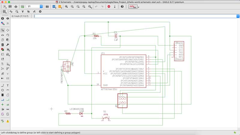
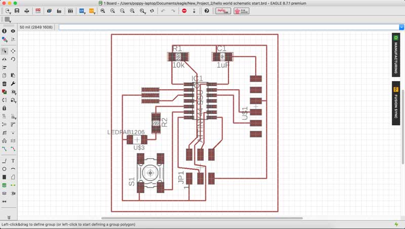
Click on the Button to go to Board View as shown on the annotated tools image earlier on. All the components will be randomly placed at the bottom left hand side of the screen. Use the move tool to position them where desired. Faint gold lines show where conductive traces need to go. Use the Line tool to connect the components together. Once a connection has been made, the gold line will dissapear. You do not have to follow the route of the gold line. Use the rotate tool, if it makes the connections easier to route. This is where it is important that the lines do not overlap or are positioned too close together, otherwise it will cause a short in the circuit. If necessary, you can add a 0ohm resistor to act as a bridge over a conductive trace.
I found a useful technique was to be spacious when laying out the components, that way it makes it easier to rearrange things and find the most efficient route. You can always move components closer at then end, if it's necessary to save space.
Creating the Cutting Path
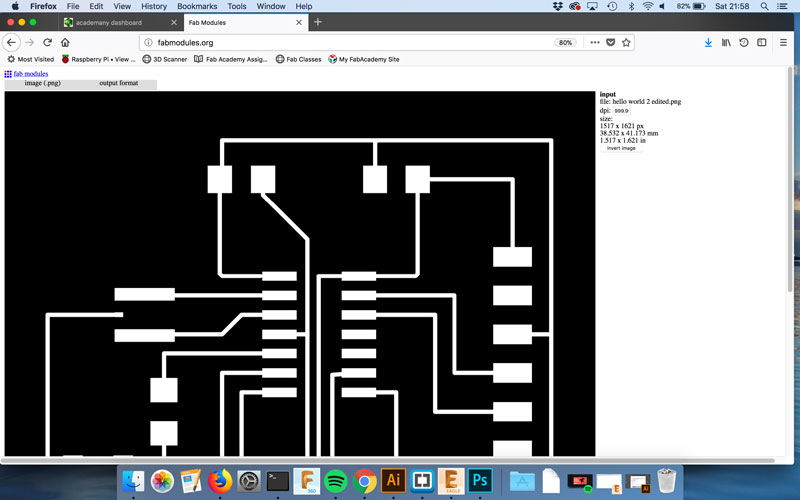
Our FabLab decided to use www.fabmodules.org to create the cutting path files rather than the newer version http://mods.cba.mit.edu/ because it is easier to get to grips with as beginners.
- Go to www.fabmodules.org
- At the top of the page, click Input Format > Image (.png)
- Find the png image
- Click Open
- If the lines are in black, click Invert Image on the right hand side
- At the top of the page, click Output Format > Roland Mill (.rml)
- At the top of the page, click Process > PCB trace (1/64)
At the right hand side of the page I choose the following options (although some of this will be different depending on the tool used):
- Machine: MDX-40 (ours is a MDX-50 but the same settings work
- x0(mm): 0
- y0(mm): 0
- z0(mm): 0
- zjog(mm): 2 (this is the height the end mill will be at when it moves around in between milling
- xhome(mm): 0 (home is where the end mill will return after milling
- yhome(mm): 0
- zhome(mm): 2
- number of offsets: choose a number: -1 will remove all unused copper, 1 will go round the traces once, 2 will go round twice etc. I went for 4.
- Then click Calculate
- After a few seconds, the cutting path will appear
- Click Save
Milling and Soldering the Board
Please see Week 5 - Electronics Production for details about milling and soldering.
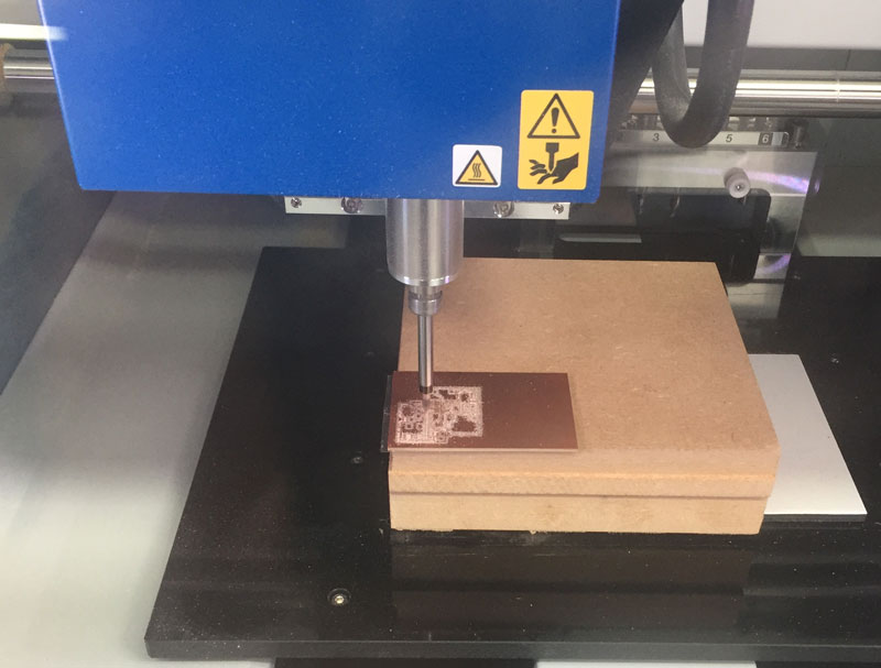
A description of my soldering process is in Week 5 - Electronics Production
