Théo Lepage-Richer

Fab Academy / Digital Fabrication 2015

Designing and Making One’s Own Fabduino, and Resisting the Urge of Calling it the “Fuck-it-duino”

This week’s assignment has been, for me, the most time-consuming, effort-intensive and overall… anticlimactic one of them all. As my mind is, like I first mentioned last week, slowly settling on building a rotational casting machine for my final project, I dedicated the input and output device weeks to making bits and parts of it. In that sense, I decided to make a system able to translate inputs from a potentiometer into motor velocities and, to make everything easier (well, that was the initial intention), started working on my own version of the Fabduino as a way to bring together these inputs/outputs.

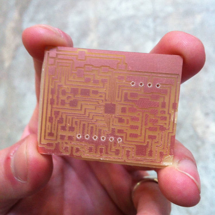
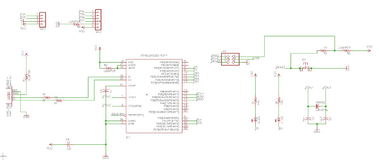
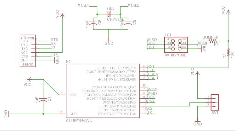
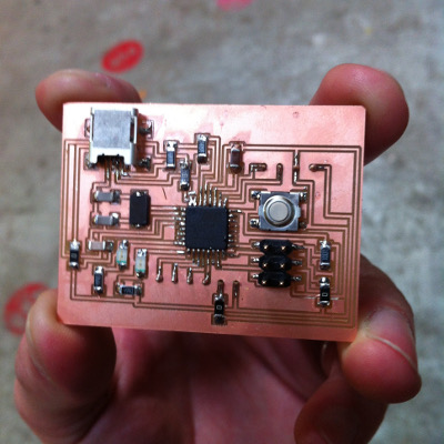
I therefore spend most of the week designing the said board. Ferdi recommended me to work with the USB-enabled ATmega16u2 chip, which I welcomed as an interesting challenge for I couldn’t find any similar fab-board using this chip. The first half of the week was pretty much a big puzzle, as I could only loosely inspire myself from Neil’s Fabduino, Fab Lab Barcelona’s very own Barduino, and the schematic of Arduino’s Leonardo board, which relies on the same chip. I therefore became quite close with the ATmega16u2’s datasheet (marvelous bed-side table reading) and tried to fit as many ports, bits and pieces as possible on the smallest surface I could make them fit. I was indeed quite happy of the resulting size which was something like 1.35 by 1.42 inches, but ran into my first major problem at this point when I realized I had been designing my board with the ATmega16u2 mini schematic, and not the bigger one that we keep in the inventory.

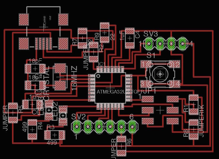
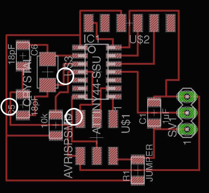
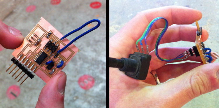
This first hair-raising pickle put behind me, I quickly redrew the whole thing with the bigger chip and milled it using the 0.010 mill – the smallest one that we have in the inventory. I indeed had to reduce the size of some bits of the sketch directly on GIMP so it could be cut in the Modela, but the milling went quite well otherwise – using the 0.010 for the traces, the 1/64 for the holes, and the 1/32 for the outline. I then could solder every piece on the board, which went surprisingly well despite its small size – I really feel like I am getting my head around soldering.

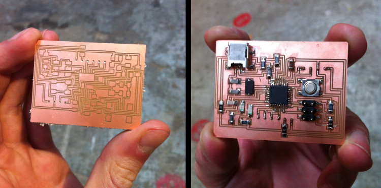
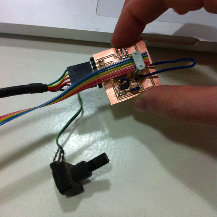
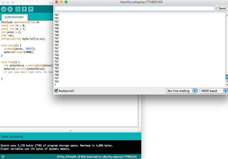
Unfortunately, as I was running short on time, I couldn’t really test my board – it was already Tuesday at this point, and had to think of a plan B in the very likely possible of the board not being usable in the short run. You can download the schematics and the board files here, but I will probably have to update them next week, as I will (quite certainly) find mistakes in them. In the meantime, I quickly designed a second, smaller board with the ATtiny44, a 16MHz clock and some inputs to connect a potentiometer (click here for the files). At this point, I was getting quite anxious of milling, soldering and making the whole thing, and, unsurprisingly, made few design mistakes (I had some lines connected where they shouldn’t have been – always do your design rule check, kids) that I could luckily get across with some jumpers. The resulting piece is quite ugly, but it’s working – I had spent so much time on my own Fabduino (still need to get a name for it, if it works at some point) that I couldn’t really spend much time on C, C++ and Python, so I simply wrote a simple Arduino script measuring and writing using serial communication the "twist level" of a potentiometer (available here), which worked smoothly.

Let there be Input from Theo L. Richer on Vimeo.

Next week, I will finally try to program my Fabduino (so far, my computer recognized it as a USB device, which is already a big victory) and come back with more news about it. Hopefully, I should be able to use it to bring my input and output devices project onto a single board!

See below for all the details/for each step.

Your Name

  • Week: 10
  • Subject: Input Devices
  • Tools: Eagle, GIMP, Modela, Arduino
  • Objective: Measure something: add a sensor to a microcontroller board that you've designed and read it
  • Files: Click here

Project 01a
The main challenge in designing a board using the ATmege16u2 chip was to figure out how exactly to integrate a USB port within its design. The ATtiny44 and the like can indeed simulate a USB port for serial communications, but doing so, like I did during the Embedded Programming week, reduces the recommended/optimal speed of exchange from 9600 to 4800. As one learns through the datasheet, the way to connect the chip to the USB, as well as the chip’s GND, UGND, AVCC, VCC and UVCC pins together, depends directly on the targeted voltage of the board, and working with 3.3V changes completely the configuration compared to working with 5V, like I decided to do. Also, the question was to evaluate how many external connections should my board affords, as the chip technically allows for a maximum of seven analog connections and thirteen digital ones. Finally, another issue with working with such a small yet very powerful is that it is easy to design paths that are too small to mill, even for the smallest mill. When I was working with the small (wrong) chip, I actually had to draw “by hand” the chip’s pads on GIMP so the Modela could actually mill them.
Project 01a Project 01a
When I redesigned the board with the proper chip, I kept a similar configuration. I connected AVCC and UVCC together on one hand, and GND, UGND and UCAP on the other, as dictated by the datasheet for a board powered with 5V. I included a header connected to four analog pins as well as VCC and GND, and another with two digital connections in addition to VCC and GND. I ended up using many jumpers, but it allowed to reduce the piece’s size drastically – this board is indeed not as small as the other one, as I couldn’t afford spending as much time in its refinement, but I could nonetheless keep it in a relatively small format.
Project 01a
The milling itself went quite well. I had to use the 0.010 mill again, which indeed allows for a very neat job. The soldering part went quite well as well, as the two pins on the top left must be connected together, which makes it possible to solidly solder the chip at one spot before doing the rest of the pins.
Project 01a Project 01a
Like I said earlier, I just couldn’t imagine at this point having the time to test, troubleshot and program my board, so I quickly drew another one able to communicate inputs from a potentiometer to a computer. To do so, I simply had to add a three-headed header connected to GND, VCC and one analog pin, as well as a 16MHz crystal and its two associated capacitors. As I still add my other board’s dimensions in mind, I made the mistake of not leaving enough space between some lines, in the way that they couldn’t be milled away by the 1/64 mill (see circles on board diagram).
Project 01a
Consequently – in a quite ugly yet effective way – I cut the wrong connections with a knife and added three cables/jumpers that overcame the accidental connections. Afterward, I looked in Fab Lab BCN’s remarkable collection of old, dusty potentiometer, and simply soldered a header pin to each cable, with the VCC and the GND on each side (which side precisely doesn’t matter) and the analog connection in the middle.
Project 01a
In the end, I could simply connect this last board through FTDI to my computer as well as to my FabISB through the six-pinned header, and uploaded a very simply Arduino script.
Project 01a
As I couldn’t use my USB-enabled board, I had to simulate the serial communication at a software level, which went quite well, as I had already went through this process during the Embedded Programming week. My next objective is then to connect, troubleshot and program my own Fabduino board, and, ideally, redo with it the same exercise I did with my second board. If everything goes well, I should next week be able to bring this week and next week’s assignments together and directly control a motor with a potentiometer by using my Fabduino, without any serial communication with a computer.