The activity of this week was to make a PCB for a FabISP programmer.
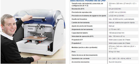
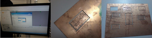
To make this a milling machine Plotter ProtoMat S43 model , which has the following technical characteristics shown in the figure are used:
To use this machine 's manual of the equipment previously reviewed before performing the initial performance tests. The software in the general procedure was as follows:
1. Bring the circuit design : in this case the Eagle program for this activity is used, as it gave us the Gerber file you need the machine to machine the PCB.
2. Using the software where the type of hardware associated with the structure outlined.
3. Detail the material with which he goes to work.
4. The number of layers of the circuit is defined : in our case a layer is used as the circuit was not very complex.
5. Using the wizard 's own machine program .
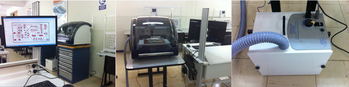
Like any machine , power supply connections are made , as well as communication cables attached to the PC. Moreover the vacuum system was engaging , whose function is to fix the plate where it will do the tracks of the circuit; also used to remove excess material ( chip ) obtained by the process.
Before giving the order of execution from the PC card is placed. In initial tests note that the suction system was not strong enough to hold the plate , so put tape " masking tape" to fix the plate at the time of machining
The machine comes with an application to machine plates , for it added the following link , where the procedure which I have followed is shown.
Welding part for supporting the video was used:
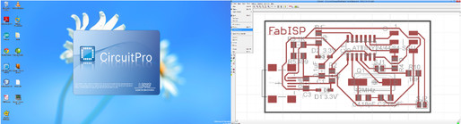
In the next picture the execution of the application of " CircuitPro " is displayed, the file from which you want to obtain the PCB is also shown.
Once the file is loaded, we proceed to place the plate and turn on the vacuum system.
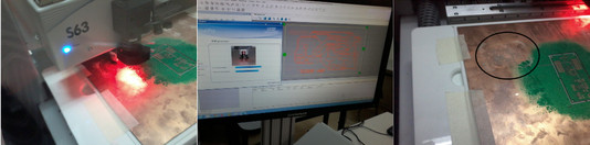
In the figure the time in which the card is shown plotting . The software monitors in real time the development process in the plate. The good thing about this machine is that you 're performing cutting plate.
The software has the advantage that gives us the time to take the machining process of the PBC , as shown in the figure is the finished board . Several plates was performed on a trial basis.
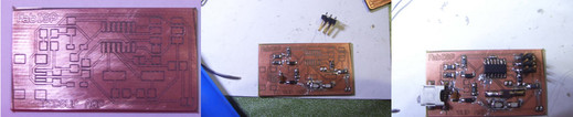
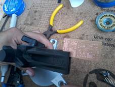
For the process of thin soldering tip soldering iron , copper cord , tweezers and electronic surface mount components are used. Moreover it took a magnifying glass with lamp installed . It is noteworthy that it was not easy to solder the components on the board , so the technique shown in the video was used as shown above text . Then verify that there were no short between tracks.
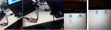
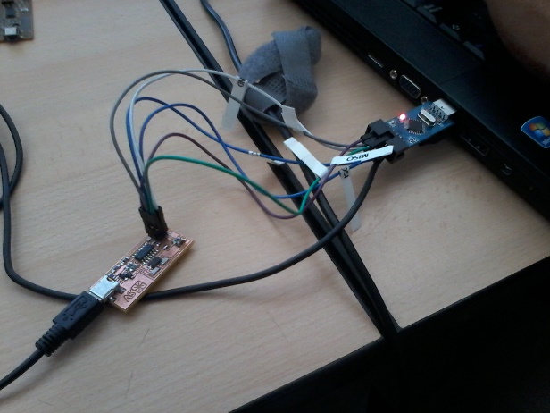
Tutorials procedure was followed links course , the activities are shown in Fig . I had no problems in connectivity and device recognition.
The disadvantage that could not download the application program in the circuit realized , since another developer was used was taken . This part remains to be completed using the charger FAB LAB laboratory.
FABISP MAKING IN MODEL
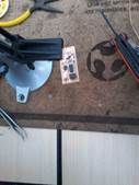
Proceeded to make a new FABISP card, in this case the machine "models " was used . For the manufacture of the electronic board two milling cutters was used as:
- 1/64 " for roughing and obtaining electronic tracks.
- 1/32 " to cut the card frame.
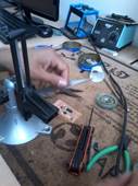
Once this is done we proceed to solder electronic components on the card. As additional support materials, solder paste, solder, tweezers, electric soldering iron was used. The developed process is shown in the following images:
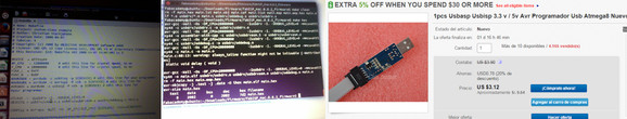
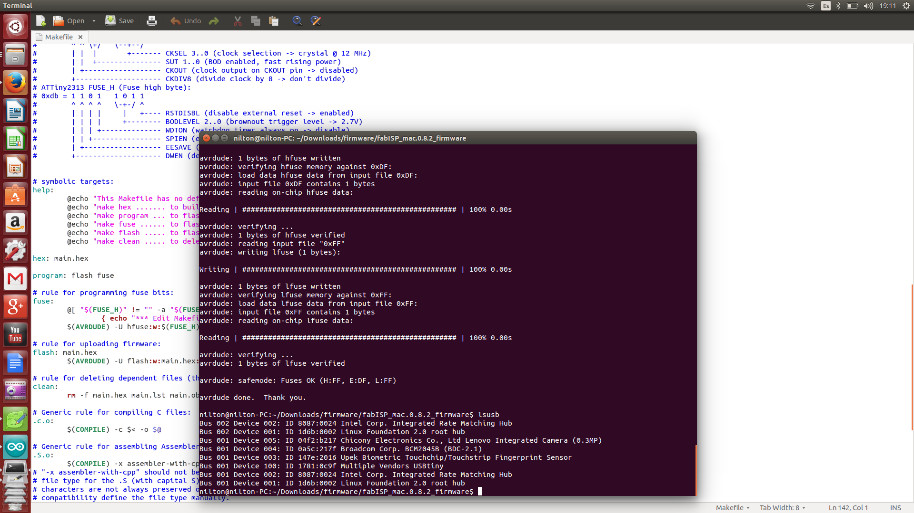
Once done this, we proceed to record the program to the microcontroller Attiny 44, for which the terminal is opened LINUX and proceed with the following commands: make clean, make hex, and sudo make sudo make fuse program. The result is shown in the following figure where the success of this step is observed. So we have a programmer microcontroller.