Since I began with The Fab Foundation, I helped support two cycles of Fab Academy. While my main preoccupation with Fab Labs is procuring and deploying inventories for new installations, I also help procure supplies for labs running Academany courses. While most requests come in the form of shipping out end mills or FR-1, the most involved request was the procurement and distribution of Stage Kits for the Machine Making assignment. It was during my second go in 2016 of shipping out stage kits that I got my first big lesson in Electronics Design.
We switched vendors to Seeed Studio to supply gestalt nodes. Not knowing any better, I did a simple git clone of the gestalt single stepper node repository and sent it along with our quote request. This was my first time dealing with a board house. Thankfully, Seeed and other such board houses provide helpful walkthroughs of the actual ordering process. Instead of referring me to such a page, the representatives at Seeed were very generous and attempted to gather the necessary information over email. They needed: Gerber files, a Pick & Place file, PCB technology specification, and a Bill of Materials. In addition to those files, they requested several changes to the gestalt node (at that time it was rev 0.3).
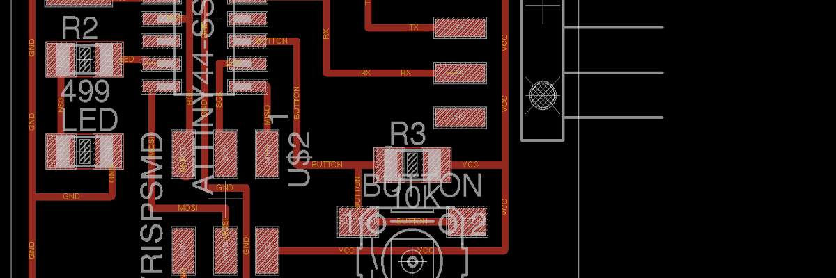
Seeed provides files on their “Fusion” ordering page which are used in Eagle CAD. There are design rules files for two and four layer boards. There are also CAM processor files to export Gerber files for two and four layer boards. The gestalt node is a four layer board with through holes. So, I downloaded the DRU and CAM files for four layers. I copied each file into the Eagle sub folders for design rules and cam processors. I made a new folder under the projects sub folder. I then copied the board file and schematic for gestalt node rev 0.3 into the new folder. Setting up the files for Eagle was all done outside in Finder on Mac OS X.
Design Rules Check (DRC) is accessible in Board View under Tools -> DRC. This will default to the Eagle Default DRC. Once the window is open, the “Load…” button gave access to the Seeed DRC. Once the check is run, the design rules are copied to the board. Running the Seeed DRC on gestalt node rev 0.3 generates quite a few errors mostly with Clearance, Keep Out, and Stop Masks.
Menus in Eagle are context sensitive (at least in Mac OS X). To export Gerber files for Seeed, (once again, in Board View) I went to File -> CAM Processor. With the CAM Processor window open, I went back to File and selected Open -> Job. This opened the cam processor sub folder and I was able to load the Seeed Gerber processor. Eagle does include Gerber processors. Depending on the board house, you should download and process your PCB design according to their requirements. One of the best explanations that I found of Gerber files was on Maxembedded.com. In an article describing PCB Design, Soumil Heble says that Gerber files are PDFs of your PCB for manufacturers. These are final copies of the layers that are not meant to be edited. So, what happens when your Gerber files cause problems for the manufacturer?
In my haste to meet a deadline (fabrication and shipment of boards from China to Boston take up to five weeks), I neglected the list of Design Rules errors. Seeed did have the Board and Schematic files for the gestalt node rev 0.3. So, they were able to supply a Design For Manufacturing (DFM) Feedback Report. This report of issues was categorized by level of seriousness between cool and hot. Hot meant the issue was a “manufacturing or reliability show stopper”. Cool meant the issue had a “low impact on cost, quality or cycle time”. Nothing on the list was Hot; yet, minor moves and adjustments needed to be made to address issues that were “Warm” or “Cool”. The issues were: “0805 package distance is too small, recommend to adjust to 0.75mm; silk screen are still on pad, need to move; There is no direction mark of IC6; Via holes are on the pad, need to move.”
We facilitated a little back and forth negotiating between Seeed and Nadya Peek. Adjusting the location of the 0805 package components would have required Nadya to change the board significantly. Seeed confirmed that we were able to go ahead with the present pad positions. The reason for such clearance concerns is that components of differing signals could influence each other if spaced too close. By Seeed’s rules, the components should be spaced 0.75 mm apart. Still, we were able to go forward with the job by only moving the silk screen and via holes away from the pads. We also added a direction mark to IC6. With those minor adjustments, we had gestalt node rev 0.4.