Electronics Design
Designing
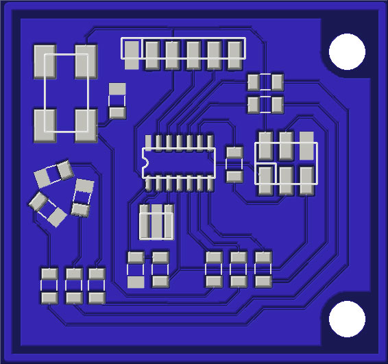
The board, designed in gEDA:
First tried the cad in the compiled fab modules, but found that it took me a considerable amount of time for adding each wire (and the points too). Too slow to make a change, then press a button to refresh, then make another change -- when a mouse could be used. So switched back to gEDA.
Downloaded some of the relevant footprints from gedasymbols.org. The ISP and FTDI header needed fixing. Referred to the land patterns document, and fixed them with a text editor. Had to make the button and crystal footprints.
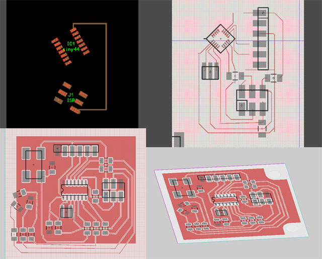
Photo above:
Top left: components on an angle in the fab modules cad
Top right: trying the qfn version of the ATtiny44 -- the routing didn't work out
Bottom left: everything is connected, still have to clean up the routing
Bottom right: cleaned up routing and looking at board in gEDA's "3D" mode
The traces were 6 mil with 6 mil clearance. If the traces need to be changed for a specific machine, this can be done by changing the Line[...] items inside of Layer(1 "top").
The copper fill is a ground plane. Some of the pads connect to it (tricky to see in first photo)
Fabricating
Will be doing this when going to EchoFab.
Design Files
You can find all of the source files in my repository