About me
Final project -
development
Final project
Weekly projects
Wk 13 Networking and
Communications (Apr 29)
Assignment:
• Design and
build a wired &/or wireless network connecting
at least two processors
Background
This week, it was suggested by our tutors that
it might be an opportune juncture to present to
each other, our current vision of our individual
final projects, including our understanding of
what inputs and outputs we would need to achieve
our objectives.
This was a great idea, as in this way, we
benefitted by:
• receiving constructive feedback on our concept;
• receiving questions to help reveal or deepen
areas we may not have considered;
• knowledge from our tutors on
electronic/maufacturing know-how;
• learning more about what technology would be
required (hardware/software);
• reflecting on our Networking and Comms
requirements for this module.
As a beginner in electronics,
for the Networking and Communications assignment
this week, I chose to make 3 boards as part of the
hello world example.
The purpose of this hello
world example
is to network several boards together in the form
of a serial communication bus (as opposed to
parrallell communication - think two-way country
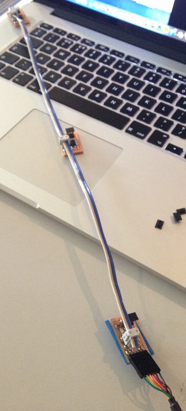
roads vs 8 lane motorway). The bridge board
(which is also a node) is connected to a computer
via a FTDI cable. The two other node boards are
connected to the bridge board.
To make efficient use of milling time and
materials on the Modela, it was suggested that all
the two different types of boards required for our
group were milled in succession, on a single
larger board. This meant that we all hit the
soldering stations at the same time and were able
to be more efficient.
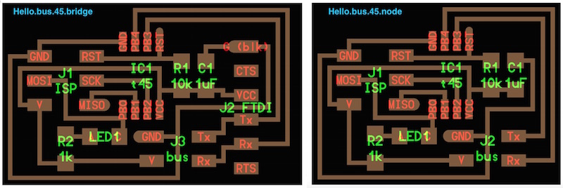
For reference, here below, are the sample boards
(bridge and node) used for this week's assignment.
It was noted that the
only difference between the two boards was
the FTDI connector added on the 'bridge':
Below, the boards have been milled, soldered.
Each board would need to be given a node ID number
or "character" (ready to be identified in the
programming):

A visual inspection was made of all boards, and
they appeared ready for cable connection and
programming.
Programming
the boards (see tutorial)
This involved downloading the
"hello.bus.45.c" and "makefile" onto my
desktop, saving them into a dedicated
folder, then renaming the downloaded
"hello.bus.45.make" as "makefile".
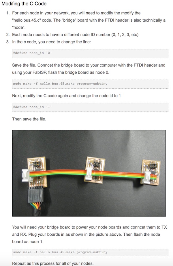
The C code file was modified so that each
of the nodes (including the bridge) could
be identified as a unique "character" on
the network and communications (as
mentioned earlier). So, starting with
identifying the bridge as "0", in turn we
identify node "1" and then, furthest away,
node "2". This is shown in more detail in
the screen grab from the tutorial below:
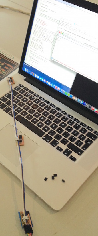
I connected my Fab ISP
to the network, connecting power
from my laptop, and succesfully
programmed each board in turn.

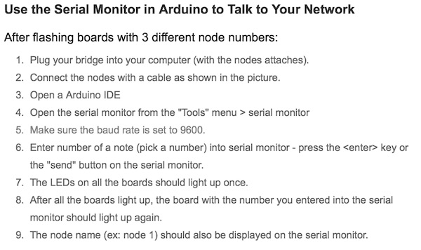
The next stage was to use the "serial monitor" in
Arduino to communicate with my network. Again, I
inlcude a screen grab of the instructions from the
tutorial to do this. See screen grab below:
Here are the successful results from the serial
monitor test:
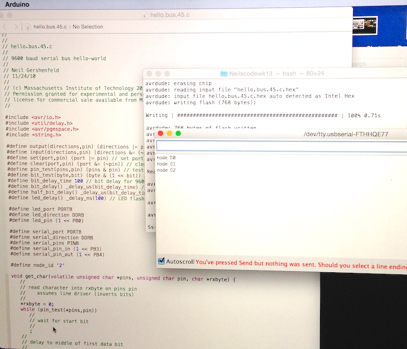
When character "0" was pressed in the serial
monitor, the led would flash on the bridge (named
"0"). When character "1" was pressed, the led
would flash on node "1", etc.


