EAGLE INSTALLATION AND WORKFLOW
TUTORIAL PICTURES:
- Download the Eagle Freeware Version and install
- Download the Fab Libraries with inventory of many useful parts
- Also keep an eye on the Fab Inventory spreadsheet which contains a list of all parts with codes and suppliers
- Create new project:
Opening Eagle and create a new project in FILE> NEW PROJECT
Within the new project you can create a new SCHEMATIC and BOARD
- Import the libraries:
On Mac the lbr (libraries) folders is in APPLICATIONS> EAGLE-7.2.0> lbr
You can drag all your downloaded libraries here.
To activate them, in Eagle IDE go to LIBRARIES> USE> and select from dropdown menu all libraries you need
- Add all needed components we know we will be using
Follow the Fab Academy Tutorial, that gives step by step instructions. I personally used this image as a reference, trying to replicate it by following the tutorial.
In my design I decided to have 2 LEDs connected in parallel, a button, and to have access to all free pins on the ATTINY, so I added a Sparkfun female 6 header through hole connector to be able to use them.
The add button on the left of your schematic window allows you to add the elements.
PARTS
1X PIN HEADER 2X3 (for programming the board)
1X FTDI SMD HEADER (powers the board and allows to talk to computer)
1X FTDI CABLE
CABLE 10 COND 300' MULTI RIBBON
1X ATTINY44A-SSU-ND
1X M06SIP (M06) through hole (for free pins)
1X CERAMIC RESONATOR 20.00MHZ SMD
2X RESISTOR 10.0K OHM 1/4W 1% 1206 SMD
1X RESISTOR 40 OHM 1/4W 1% 1206 SMD
2X LED 1206
1X SWITCH 6MM TACTILE SPST-NO 0.05A 24V
1X CAPACITOR CERAMIC 1UF 50V 10% X7R 1206
- There is a difference between THROUGH HOLE and ON SURFACE components. In the library they might have the same name, but the through hole components have green parts (parts that perforate the board), whereas the on surface ones are all red. We mainly use on surface components (as in the FabISP too).
- 1206 are the 'biggest' components, easier to solder, so we generally use those from the libraries list
- Apart from the components themselves you will also need to add GNDs and VCCs, because you will connect lots of components to them!

USING THE INTERFACE/ SCHEMATIC
Now we can start creating connections.
Commands:
MOVE left click on the cross on object to select and move
ROTATE
SELECT GROUP
NET
NAME
VALUE
LABEL
CHANGE
INFO
MOVE GROUP COMBO:
1.select move
2.select group
3. right click + command
CHANGE EVERYTHING AT ONCE:
1. select group
2. change
3. from dropdown menu select option (ex. width of cable)
4. right click + command to apply to all
- When we create NETs, we can assign names to them (and label them so that we can visualise the names), and any other net to whom the same name will be assigned, will automatically connect to that same trace. The system will ask you first if you are sure you want to connect the two nets.
- Calculate current limiting resistor for LEDs:
In the Fab Inventory list we can find the code of our LED and open the Data sheet.
In order to calculate the resistance we need to know:
LED FORWARD CURRENT: 40mA
LED FORWARD VOLTAGE: 1.8 V
SOURCE VOLTAGE: in our case we use 5V
One LED requires a 82 Ohms resistor.
In my case, 2 LEDs connected in paraller require a 40 Ohms resistor.
- To assign to the RESISTOR part its value, right click on the object > VALUE > type the value
USING THE INTERFACE/ BOARD
We can now switch to Board design mode, and connect our components.
We will need:
ROUTE
UNROUTE
to create lines between our components.
Our traces should be 0.4064 wide minimum.
We will need to make sure that the traces are distant enough so the drill bit can pass through them at least once. Since our drill bit is 1/64 inches = 0.39 mm, we use 0.4 mm as standard CLEARANCE between traces. To check we need to run DRC > CLEARANCE > CHECK on the parts. If some connections are too close to some parts, the program will create a list of errors and show them with red lines on the board.
To change wire size for example, we can select the object, right click + PROPERTIES and edit the thickness.
To correct these errors we can use GRID, which allows us to give ourselves constrictions when moving the traces around. When moving the traces, they snap to these grids. The standard grid is SIZE 2.54 mm, but we can change it to dividends of that measure like: 1.27 or 0.63.
We can also ALT. When pressing ALT while moving our objects, we can be even more precise, therefore we can give an even smaller dividend, like 0.63 or 0.31 or 0.158.
DESIGN DETAILS
In my board design I decided to make use of all available free pins on the Attiny, through a female connector, which is quite convenient for creating shields. Female headers will correspond to:
pin 5
pin 11
MISO (used to program the boards and then free)
MOSI (used to program the boards and then free)
SCK (used to program the boards and then free)
GND
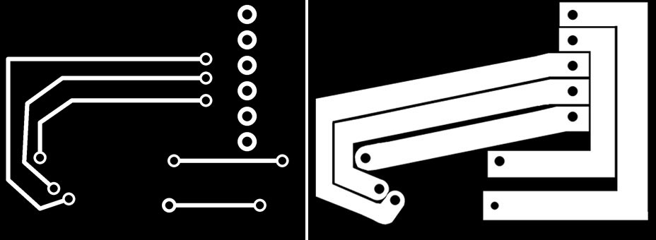
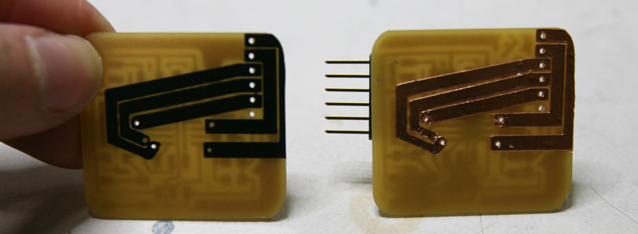
The Sparkfun component is a through-hole component. I decided to use VIAS and create a bottom layer (because I was curious of using the vynil cutter to create the copper traces for the bottom side). I created bottom layer traces that would join with top layer ones at the vias.
LEARNING:
The (final) holes I created were optimised for the 0.8 drill bit (1/32), with a diameter of 1.27.
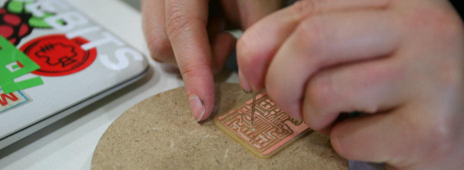
I had to edit the design of the holes many times because they were too small for a 1/32 drill bit first. I also tried to use a 1/64 but the holes were too small and nothing could go through them. I then tried to push a needle in, but I broke the copper traces and had to do it all over again...

I found it much better to drill the holes with the 1/32, because in the soldering process, where I used the leg of a resistor to connect top and bottom parts, smaller holes would not let the resistor leg through anyways.

EXPORTING THE DESIGN & MILLING
Once the design is finished we export PNG files of our design:
- Select through LAYERS option the appropriate layers to export
- 1000 dpi resolution
- MONOCHROME
- full area
In Photoshop I then created my frame, leaving 0.8 mm space on each side.
For the holes, I reversed the colours to obtain the holes in black.
Files and milling specifications:
01: external border to test z=0 @1/64 drill bit
02: top traces @1/64 drill bit
03: holes @1/32 drill bit
01: external border @1/32 drill bit

VYNIL CUTTER
The traces I exported from EAGLE were definitely too small for the vinyl cutter, so I redesigned them as big as possible (and with the least gap between each other in Photoshop. This is really the minimum size to be able to weed the parts from the copper roll.

I used FabModules to create the file for the vynil cutter.
I selected the copper default settings and diminished the drill diameter to 0.1 to obtain better resolution.
I first run a test with vynil to check my design was ok, weeded it and glued to the back of my failed board. I then cut the copper sheet, weeded it and stuck it on the back of my board. After a bit of adjusting of holes and distances between traces it works beautifully!


Files:
01: Bottom traces
SOLDERING THE COMPONENTS
TIPS:
- LED green line corresponds to ground
- ATTINY has a direction
- For my top and bottom parts, I connected the vias on the two layers by soldering through the legs of old school resistors.

PROGRAMMING THE BOARD
To check if the board works download the programs (for mac):
- Arduino 1.6
- Attiny Board files for Arduino 1.6 . I followed this tutorial to move them to the right folder. They are needed because otherwise the Arduino IDE would not give you the options for ATTINY microprocessor.
- FTDI drivers
[FROM THE TUTORIAL:]
- Unzip the attiny zip file. It should contain an “attiny-ide.1.6.x” folder
- Locate your Arduino sketchbook folder
- Create a new sub-folder called “hardware” in the sketchbook folder, if it doesn’t exist already.
- Copy the “attiny” folder (not the containing attiny-ide-1.6.x or attiny-1.0.x folder) from the unzipped ATtiny.zip to the “hardware” folder. You should end up with folder structure like DOCUMENTS > ARDUINO > HARDWARE > attiny > avr that contains the file boards.txt and another folder called variants.
- Restart the Arduino development environment.
- You should see an ATtiny entry in the Tools > Board menu. When you select it, you should see additional Clock and Processor sub-menus in the Tools menu. These allow you to specify your ATtiny configuration.
I then connected:
- the FabISP to the computer via usb
- the Hello board to the computer via FTDI cable
- and the two boards together through the 6 pins connector *MAKING SURE THAT ALL PINS ARE THE SAME!!! GROUND TO GROUND*
On the Arduino IDE, in the dropdown menu I selected:
TOOLS> BOARD> attiny
TOOLS> CLOCK> 20 MH
TOOLS> PROCESSOR> ATTINY44
TOOLS> PORT> my .cuusbserial port
TOOLS> PROGRAMMER> USBtinyISP
TOOLS> BURNLOADER
This is a table of the pins correspondance between attiny and Arduino, to program the board with Arduino IDE:
ATTINY 44A / ARDUINO / DETAILS
01 / - / VCC
02 / 10 / -
03 / 09 / -
04 / - / RESET
05 / 08 / PWM
06 / 07 / PWM, ANALOG INPUT 7
07 / 06 / MOSI, PWM, ANALOG INPUT 6
08 / 05 / ANALOG INPUT 5, PWM, MISO
09 / 04 / ANALOG INPUT 4, SCK
10 / 03 / ANALOG INPUT 3
11 / 02 / ANALOG INPUT 2
12 / 01 / ANALOG INPUT 1
13 / 0 / ANALOG INPUT 0, AREF
14 / - / GND
I used the Blink example (which is set to Arduino pin 13, since Arduino has a on board LED there) and changed to output PIN 7, which corresponds to my PIN 06 on the Attiny.

Working!
FILES DOWNLOAD LINK
HOME | ABOUT | WORK | CONTACT
Francesca Perona © 2015

This work is licensed under a Creative Commons Attribution-NonCommercial 4.0 International License
Original open source HTML and CSS files
Second HTML and CSS source
Francesca Perona © 2015

This work is licensed under a Creative Commons Attribution-NonCommercial 4.0 International License
Original open source HTML and CSS files
Second HTML and CSS source