
Electronics Design
This week, we have had to add components to a PCB-design. There are many different programs that can do this, but I have chosen to use eagle as it is one of the more established softwares and therefore has many tutorials.
After having downloaded and installed Eagle, I downloaded the component libraries that are made in the FabLab environment, with the most common components. Besides that, I also downloaded the Hello World Board which I had to work with for this week assignment. The task was adding a LED and a switch to the board, which will then be programmed next week.
Workflow
It is very new for me to work with electronics in this way. It has surprised me how simple the workflow is and what opportunities there are with these skills.
I opened the Hello World board in Eagle and gained an overview of how it operates. There after I found in the library, the components I needed.
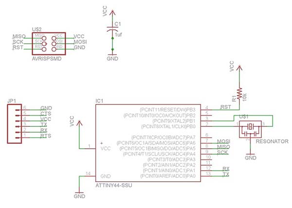
Here is the diagram that is starts with. I could see that pin 6, 10 and 11 was free.
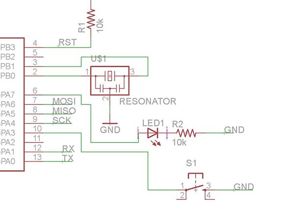
After finding the switch and the LED in the library, I placed and connected them with the free pins. When the components where located roughly I used the "wire" function to drag the connections.
When the connections are drawn, you can go to the "board" mode, where you can see the layout of the board, and the physical traces. In my case I had to relay components so the design made more sense. When the design considerations are done, you can run a debugging that tells whether the design meets the fabrication parameters you have set in advance. One of these parameters is, for example. the diameter of the cutter. It is important that the traces are not too close, that the milling-bit cannot enter in between them.
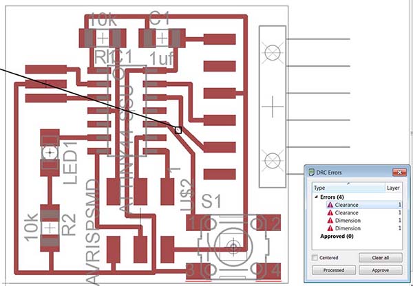
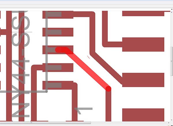
I got a total of four errors. I therefore adjusted the components and traces that created the individual errors. Here after I made a new debugging and there was no errors.
Now the PCB was designed the way I wanted it, and I was now ready to export the design as a bit-map which can be used in fabmodules where I setout to mill the PCB. Eagle can work in many layers, but it is not all layers that are important when it comes to routing the design. Therefore, you should before you make exports turn off all unnecessary layers. The easiest way is to turn them all off to start with, and then turn on the 3-4 layers you need.
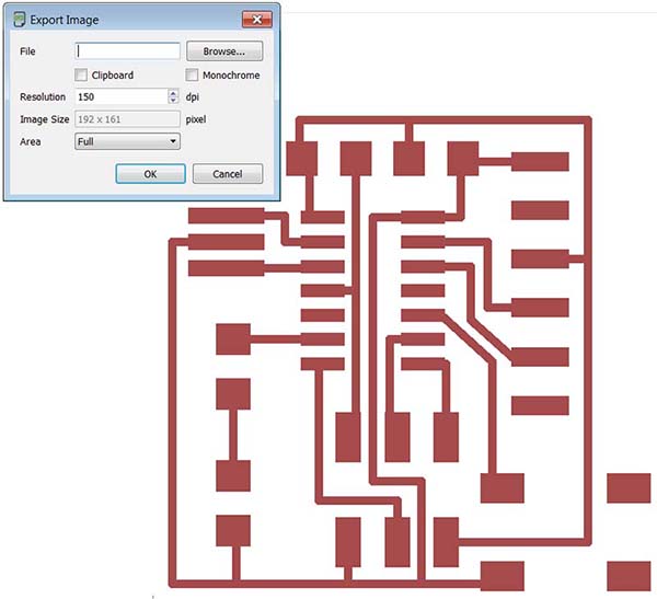
When you export to a bit-map, you must choose which resolution. Basically 500 dpi is fine, but if you are doing some more detailed designs, it may be necessary to increase the number of pixels.
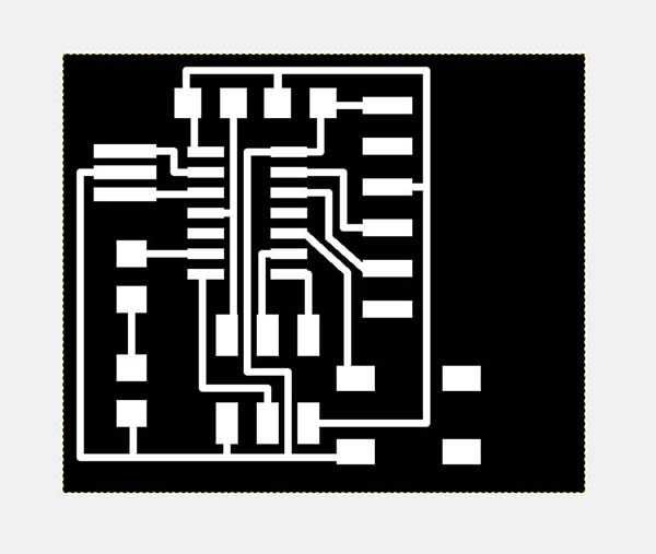
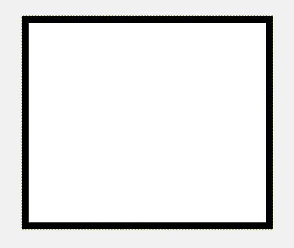
When the export is made, you have to manipulate image abot. The image is exported, is only a representation of the traces, so it is necessary to add an edge as fabmodules can use that to make the paths to mill the outline of the PCB. This is done, for example. In GIMP or Photoshop. I used gimp, where I added 20 pixels on all sides of the board.
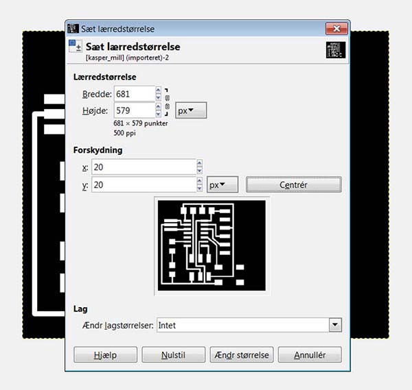
I made two images in GIMP, a picture of all traces, and a picture of the outline.
Now the PCB is ready to be milled. I refer to the description of the tasks that were solved in Week 4 "electronic production."
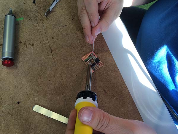
When the board has been machined, it is time to solder all the components; here it may be advantageous to print the schematic from eagle out and use it to locate all the specific components.
You can find my design files here. board and schematic .