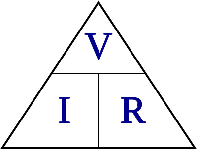
Theory
Convention is that current flows from + to -, in reality it is the reversed, it is the tiny electrons that flows and not the protons and neutrons as they are much larger.
Calculating the current limiting resistor in a single LED circuit.
LEDs are simple, and a fairly universal first electronics project. To calculate the correct current limiting resistor find the forward current and voltage in the data sheet.
(Voltage drop across an LED, also known as forward voltage, tells you how many volts are needed to light it up.)
R=(V-Vd)/Id
To calculate the resistance for your circuit subtract the voltage drop from the supply voltage and divide by the desired current.
Data sheet states the LED’s typical forward voltage is 2V. From the same data sheet the optimal forward current is 20mA. If we power this with a 5 volt supply the calculation is as follows.
R=(5V-2V)/20mS = 3V/20mA=150 Ohm
if the result is not a standard resistor value select the closest one.
If you can't be bothered with all this, just use our rule of thumb for prototype board LEDs:
You might have noticed that these values are much smaller then the rule of thumb values we gave earlier. This is because we don't want the LEDs to be at full brightness. It's often distracting to users.
It also doesn't matter if place the resistor before or after the LED because is the amount of current the resistor limits as not to burn the LED. In a series circuit the current is the same for all components and because the LED and the resistor are in series you can connect either way.
Links
Kirchhoff's First Law
The algebraic sum of the currents flowing through a junction is zero. Currents approaching the junction are + while currents going away from the junction are -
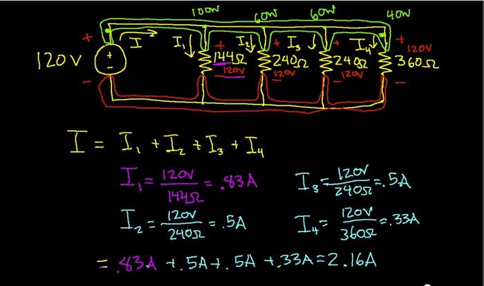
Kirchhoff's first law when officially stated (see link) sounds more complicated than it actually is. Generally speaking, it says, the total current entering a junction/node must equal the total current leaving the junction/node. After all, no charges can simply disappear or get created, so current can't disappear or be created either. A junction/node is any place in a circuit where more than two paths come together. Or to be more precise, a node is not where the wires, a node is all the wires up to a component, see images below. Kirchhoff's first law animated.
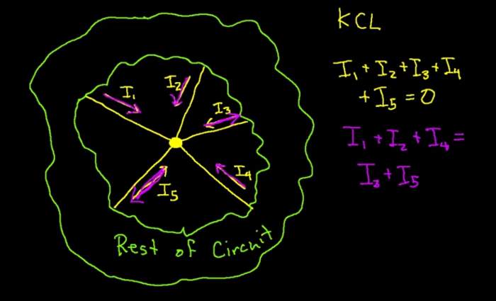 Current is dividing itself taking differet routs out of a junction.
 Here drawn in green is one single node and red is another .
Designing the Hello board in Eagle
I started to watch a tutorial on Eagle to get the basics. With the imported Fab library I creating the schematic with the button and LED added. It was a bit confusing but not to difficult. Routing the board how ever turned out to be much more difficult
Dragging nodes and connecting the dots was at first very enjoyable and big plans of making a pretty layout was drafted. But after over an hour of trying to find the perfect layout without crossing lines or make a two sided board I reverted back to KISS principle (keep it simple stupid) I customized my own short cuts under option/assign to speed up the work flow. It will really speeed up your workflow.Started to routing with 0.6096 line width. But theses where to fat to fit 3 lines under the IC1 so I change it to 0.4064 and with some manual tweaking it was just possible.
In summary I liked it . A lot of micro management with some frustration of lines not connecting properly but just lying on top.
I continued to export a monochrome .PNG at 1200dpi opened the file in gimp and made the exterior cut a selection and stroke. (did not realize I could just have exported the dimension layer)
Milling the board was straight forward but here I realized my mistake! One of the rout was to close to the pins so the end mill could not go get between them... but nothing a xacto knife could not fix. Coming back to Eagle and tweaked the spaces between the lines under the IC1 and double checked it in the Fab modules so it will work for the next board. for now keep moving forward.
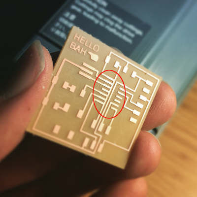 The VCC rout was to close to the pins.
 Result after operation.
So what I should have done to avoid this problem was to 3. Load Design Rules In order to make sure the PCB we're designing can actually be made on the milling machine it will have require a certain spacing between paths and pads, the milling bit will have to fit in between. First download and save fablab.dru (link at bottom of the page), a set of rules created by Marc Boon. To load these rules we'll have to click the DRC tool. Then press the "Load..." button and load the fablab.dru rules. Once loaded press the "Check" button. No messages should appear, although if you use very small components there might be clearance errors.
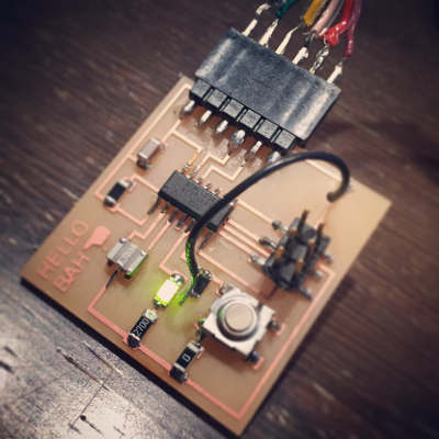
Does my Hello board work?
I connect my ISP (programming) and the FTDI (power and communication) board I my made in week 4.
Following tutorial of Scott Zitek: link I downloaded a AVR assembler Gerd's AVR Assembler and installing it.
With the help of Francisco I wrote the assembly code in Sublime text 3 and saved it as an .asm file.
Next step was to compile the .asm file with gavrsm compiler. In the folder where I saved the blink.asm file I run gavrsm (through terminal) with the command gavrsm blink.asm. (gavrasm 'filename.asm') This creats 2 files in the same folder, a .hex and a .list file
After that I created (modify) a make file. In the same folder as the .hex and.list file. From terminal I run "make fuse" (fuse to initialize the board run once and "make program" (commands that are defined in the make file) this copies the assembly code over to the ATtiny44
The force is strong with this one.
A misunderstanding of the how the pull down resistor works made it possible to turn the light on just by having your finger close to the button. What I had was made was pin to button to resistor to ground in a series. not connecting the resistor to VCC before the button.
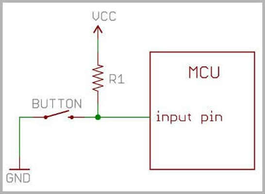 This is how a pull up resistor is designed
 Fixing mistake with solder jumper.
Now working as it should.
Other Softwares
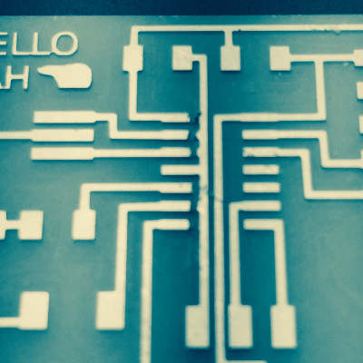
The sweet vanilla smell of Kokopelli and (local) Fab modules
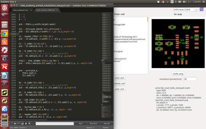
Next up I re-drew the hello board with Kokopelli and Fab modules. In the beginning it was a mouthful and it looked impossible. But slowly and over many hours I got to grips with it and finished the board.
We did not have the older version of Kokopelli where the board updates automatically as you write code. So the solution was to write code in Sublime test have the .cad file loaded in Fab module click reload file and make .PNG. Not optimal in any way but I hard core enough to write code in the tiny monochrome window of Fab modules. Thats level 40.
I like the fact that it is so simple, and with simple I mean that everything is included in the text file and you are not bound to one software to open and edit that file. It took me longer and you really need a clear idea of what you are doing. Moving things around like a puzzle game works fine in Eagle but is a pain in Kokopelli. However if you got a structured plan linking components to each other it becomes really powerful.
Some hard learned lessons where:
Update: Here is a download link to the old Kokopelli Retro download
Kicad
Kicad is an EDA software suite for the creation of professional schematics and printed circuit boards up to 32 copper layers with additional technical layers. KiCad runs on Windows, Linux and Apple OS X and is released under the open-source GNU GPL v2 free of charge.
I really liked working with the schematic. It is super fast to add your components and get them down on your schematic. As with Eagle it to got some weird user interactions, but there are some super short cut which really speed up the workflow. I had some problem of connections not sticking to the pins and it gave me errors that things where not powered. This seems to be a common problem and the solution is to make a PWR_Flag where you want power.
In Kicad you add generic components and when your schematic is built you have to define the pads for your components, before you can go to PCB editor. Here I ran in to problems as I did not have the parts/pads we use. I tried to just go with alternatives but it all became a mess.
C'edric Doutriaux was kind enough to share his Fab Kicad library with me. I have not tested it yet but he says it works but the pads needs a bit of modification. you can find it in the download link at the bottom of my page.
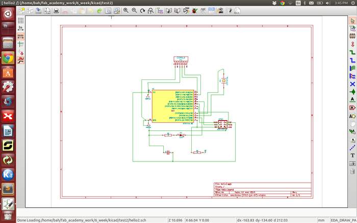 Kicad schematic view.
123D circuit
Circuits.io was bought by Autodesk some time back and is now running under the 123D circuits. It is all free and runs in a browser. It got a virtual breadboard with simulation, component editor,schematic editor and PCB editor.
Also here where the schematic editor quiet good. Adding and connecting components. How ever moving components around after they are connected gets really messy. The biggest drawback is that you can't specify what your component you want, so it is not really useful for our purpose.
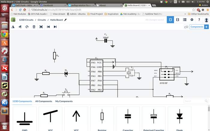 123D circuit schematic view.