This week I have to modify an existing circuit adding [at least] a button and a LED. After changing the schematic it should be milled and, then, all the components welded.
Learning how to use Eagle
This was not my first time using circuit design programs such as PSpice. But, since I was going to use Eagle the next few months for designing the circuits, I decided to create the Hello World board from scratch.
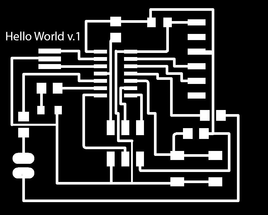
Placing all the basic components of the Hello World board in the schematic was the first step. Once I copied Neil's board design, I added a button and a led with the needed impedances. I did this before designing the layout of the board, so I didn't have to reorganize all the components.
Once I realized that two pins of the microcontroller were not being used, I added a two port connector. This will add to the board the potential to be expanded in an almost infinite number of ways. Hopefully they will be useful.
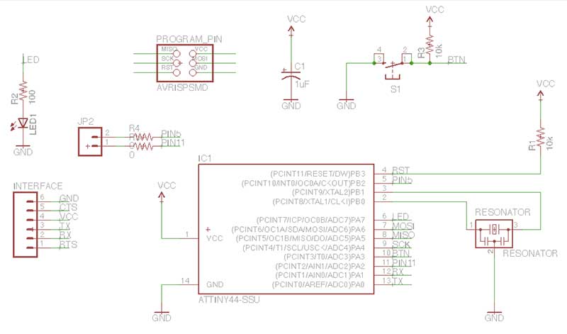
Then it was time to design the board. After reordering the components several times, the connections between them resulted in a design that didn't have crossing wires. In order to avoid those crossing paths, I had to add some bridges, so the two pin connector could be added to the board. I did those bridges by adding two 0Ω impedances.
A few minutes later, the board design was finished. Everything seemed correctly connected.
Checking the errors
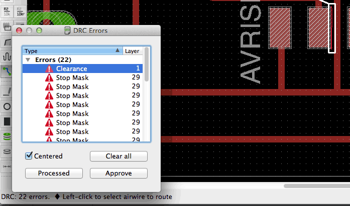
Before creating the *.png file I checked the error list. Unfortunately, a "Clearance" and several "Stop Mask" errors appeared.
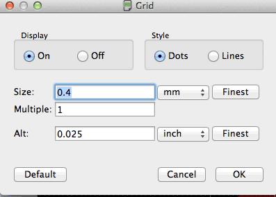
The "Clearance" error was quite easy to fix. I moved the path a little bit to the right. At first the program didn't allow me to perform the operation without changing the predefined parameters of the grid. Once I changed that parameter I was able to move the path as desired.
The second error confused me a little more. After some research, I discovered that the error came from the layer 29th (tStop). This layer would be significant if I were using other board printing techniques. Once that layer was disabled, all those errors disappeared.
Milling and welding the board

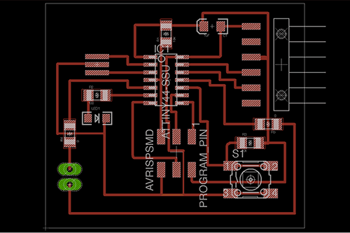
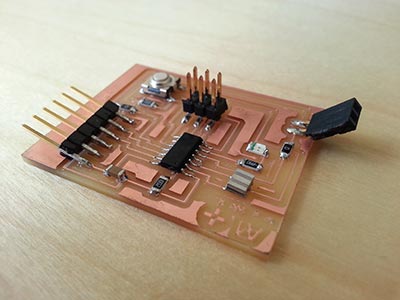
Once I exported the layers 1 and 17 to a *.png file, I decided to add the version number in the upper left corner. Using Gimp I added the text and a logo.
Milling the board was quite straightforward. I followed the same steps that were used a few weeks ago in "electronics production". But I had a problem. The version number of the board was not properly milled. The font size I used was not big enough to be milled using the 1/64 drill.
Finally I welded all the components. Everything seems connected... Will it work?
Heating or cooling an incubator needs more power than the rest of the circuitry of the device. The Peltier device needs 12V at 6A to work properly.
I had two options to deal with this device:
- Using a high power Mosfet with diodes to avoid inverse currents
- Using Relays
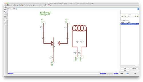
I decided to use two relays V23092-A1012-A301. Unfortunately I didn't find any eagle library with its footprint. So I decided to create my own element.
To learn how to build my own component, I watched this youtube video:
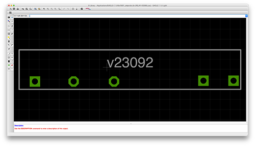
The component can be downloaded below, under the "files" section.