
Loes Bogers
FabAcademy 2015
Week 06 - Electronics Design:
Eagle, milling etc
Assignment: Redraw the Echo Hello World board. Add at least a button and an LED (with resistor), check design rules, make the board. Optional: simulate it. We'll program it next week
Back to electronics school with Emma
I've done some work with electronics during my MA and in my work but it's been a while so I decided to go to a refresher day at my local lab to get back into the mood, the physics and the formulas. Oh and here's a resource to explain some as well Electronics for Dummies (pdf)
Some definitions
- Circuit = is a closed loop that electrons can travel in.
- Current(I) = electrons flow, always from + to -. Rate at which charge is flowing. You generate it simplest with a battery and a resistor. Unit of measure is Ampere.
- Voltage(V) = difference between two points (the - and the +), it's not an absolute value. It's the difference between VCC (plus of battery) and VGND (minus of battery, eg. 9-0) But remember! Don't just look at + value, it's the different (GND is not always 0).
- Battery = power supplly of circuit, has two sides: plus (VCC, V+, +V) and minus (GND). Unit of measure is V(olt). It has an orientation
- Resistor = reduce current flow, and, at the same time, act to lower voltage levels within circuits. Unit of measure in Ohm. Has two sides, no orientation.It gives obstacle and in the electrons' flow (the current)
- Resistancy(R) = material's tendency to resist flow in a circuit, measured in Ohm.
- Ground = lowest voltage you have in a circuit. More than often it's 0, but in more complex circuit it doesn't have to be. You can hav emore GNDs in one circuit.
- Power(P) = how fast electrons are moving. Unit of measurement is Watt (W). If it is high, circuit gets hot. If power is higher than power specified in a component, the device burns.
- Schematic Is a symbolic representation of a circuit.
- Board Layout = how components and traces will be laid out on the board
Laws, relationships, equations
- Ohm's law = voltage, resistance, current. Voltage(V) = Resistance(R)*Current(I) or V=RI. So also: I=V/R and R=V/I. You need to know this because every component has specs (see its datasheet) that define what it can handle (eg. microcontroller can take max 5V), so to design a circuit that works you have to calculate these.
- Power(P) = V*I (or: Voltage(V)*Current(I))But you can take this further because if V=R*I then P can also be equalled with P=(R*I)*I or, P=R(I^2) or I=P/V. Eg. Resistors will specify how much Watts (power) they can max support)
- Current= I=P/V or I=V/R
- Kirchoff's Law = when you have a crossing of connections, the current (I) that goes into the crossing = equal to sum of currents going out of the crossings.
- In parallel vs in series: There are different ways of connecting components: in series or in parallel. This has consequences for the current in the circuit of course. If you connect batteries in series, you'll get higher voltage for example (9V + 9V - 0V = 18V).

Components
- Tact switch: is physically always open, as long as you keep pressing it, it closes circuit. Note: place switches closest possible to the high voltage! Then you make sure there's really no supply of voltage going into circuit if you don't want it: 0V everywhere please.
- Slide switch: this switch is either on or off and will stay there. Note: place switches closest possible to the high voltage! Then you make sure there's really no supply of voltage going into circuit if you don't want it. 0V everywhere please.
- LED: Light Emitting Diode. Has an anode and a cathode. Current flows from A to C, so anode goes closest to the VCC (plus). Read the symbol like a funnel: widest part first (+ or anode), narrow part is out (- or cathode). In datasheet: look for Vf or Forward Voltage: the max voltage at sides of LED when there's current through it. Also look for If or Forward Current, (see datasheet: Current Test): the maximum current you can attach. Generally, a LED accepts 5mA of current (I). The LED has negligable resistance so you don't have to calculate it (current will only be a bit lower, which is always safe, your LED might be less bright but you will hardly see that. You can take it into your calculation: then look up Vf in the datasheet to calculate actual resistance. If LED is not bright enough, you can lower resistance (be aware of limit). The stripe on the LED marks the anode (or - side). The resistor can be placed befor OR after the LED, so at all times look at the GND to determine orientations
- RGB LED: three LEDs in one. Has three legs and GND. With it you can produce all colors by regulating current per color R(ed), G(reen), B(lue). You need a resistor for each color (so 3: one for R, one for G, one for B). With a three point switch you can alternate between colors. But you can also mix the colors into one. There's RGB LEDs with a common Anode, and RGB LEDs with a common cathode, watch this to get right orientation!

- Microcontroller pins are High or Low, as with Arduino (5V or 0V)
- Capacitor: is energy storage. Unit of measurement: Farad (usually in nano, pico and microfarad. Higher gets dangerous.The current doesn't flow through, they jump in and stay there, for emergencies :D but only very little. Eg. unplug something, light takes a second or two to turn off. Polarized (has orientation) vs non-polarized: you use the polarized one as throughhole device
- Crystal resonator: unit of measurement: Hz (frequency). Used to generate a clock for the microcontroller, you will need a resonator. A "clock" means, signal that changes regularly; a periodic signal alternating high and low, like a metronome. Useful inside a circuit, but also for communication with another device.
- Diode: there's different kinds; LED, Photodiode (opposite of LED), Schottky diode, Zener diode. All characterized by Forward Current, or a forward drop.
Reading a diagram in Eagle
Take into account the laws when reading. Here's some signs (may look different in Eagle)....

- Look at name & value of the component, these are pretty standardized. Eg. R1: 10K, IC (integrated circuit, usually microcontroller).
- Voltage nodes: eg VCC, 5V or V+ for supplies. And GND or AGND for ground
- Tags you apply tags to connections between component, rather than draw actual lines, to keep it cleaner. Some of these names are standardised.
- Nets & Junctions: when two lines are connected there is a dot. No dot? then the lines may cross but they are not connected.
- Schematic vs Layout: the schematic is symbolic representation (of how the circuit works and is connected). The layout is how the actual components will be layout on a board.
- symbol vs footprintsymbol is icons in the schematic. The footprint is what the actual component looks like, how much space it needs on a board. That's why important you select exactly the right component. Eg. we use resistor1206.
- Eagle libraries: most manufacturers of components also provide Eagle libraries with symbols and footprint that match their products. Use ng.lbr (neil's), fab.lbr and RCL.lbr. Be sure to choose the 1206 components.
The Assignment
I used this tutorial page to go through the motions. And also looked at these general eagle video tutorials (really good!), and these two videos: number 1 and number 2.
A quick overview from Emma's demo:
- make new project> New > project. Go to project, go inside: > new > schematic. Also create a new board (toggle views and it will ask you to create one from the schematic you're making
- libraries Use FAB libraries, NG lib, and RCL libs to be 'safe' that the components are available in fabinventory. Always go for 1206 components, they have the right size, and make sure you pick surface mount things and not through hole depending on your board plans.
- put symbols on schematic til done with the Add tool. Give values and names.
- Creating connections with nets toolmake connections between parts to connect them. Create dots on crossing lines to connect them. Use Nets tool to do make connection nets. Name then to make sure components are connected to the right groups (see tutorial vid 1).
- Run > Tools > ERC (Electronic rules check) from schematic view and fix any errors that might pop up.
- designing board Then switch to board view: Yellow lines are connections, but these are not traces yet.
- Use the Ratsnest tool to simplify your layout.
- Align all components neatly with some space between
- Optional: for vinyl pcb:Edit > Net Classes > 0.1mm for all to set settings before using autorouter
- Use autorouter (yellow lines turn red), or do it by hand with "route" tool. Tutorial recommends 7 mil routing grid because it's the default for board houses. Be sure to set the bottom layer to N/A or it will trace the board as a double sided board! Vinylcut circuits need at least 1 mm. Download fab.dru to make sure you have modela rules find them here
- Ground plane You can make a ground plane to cover the board in copper (less milling) and add gaps to disconnect stuff from GND. It looks nicer I think: Use polygon tool, select top layer, make sure "keep orphans" is on. Set the width (the tutorial use a 10 mil width and a 12 mil isolation when working on a 7 mil grid. 7Mil distance is what board houses often require. Create a closed outline on the outline of the board. It should snap to a dotted line when closed. Use name tool and name polygon GND - don't forget this! Use Ratsnest tool to fill polygon. When closing and reopening program, you have to do this again.
- Run Design Rules Check DRC command from board view: is list of rules you want your layout to respect, eg distance between traces, how wide the traces should be. It checks it for you.
- make the board smaller, so it everything just fits
- Check layers of the file: top layer and bottom layer of the board (for double sided)You have to make sure the right stuff is on the right layer. You have to activate the right layers to see them. > apply
- Then design a rectangle in a layer that is not being used. Make it a few mm bigger than the board. Then deactivate the layer (so you don't see the rectangle anymore. You need this because otherwise you won't see the outline of the board (it will be the border of the file).
- Generate the trace file: with Top, Pads and Vias layers (usually anyways)>apply > export > image > monochrome > resolution 1000 > save as [circuitX_top]. This is the file for the traces. It will have the exact size of the hidden rectangle
- Generate the cut fileSelect layers Pad & dimensions > apply > export > image > monochrome > res 1000> save as [circuitX_cut]. This file will have exactly the same size as the invisible rectangle again. it needs the profile line to recognize it as a cutting board. If the profile = equal to edges of the file, it won't see any outside line to cut (so you draw a bigger rectangle so the profile inside it is visible to machine).
- Modify the cut file in Gimp/photoshopthen you have change the inside of the rectangle in the CUT file to white (don't invert it): board will be white, outsides will be black
- Optional: add text to board make it very thick with wide spacing. Choose "vector" and at least 1.016 size so it cuts.
- Optional: hange outline of board: go to the "Dimensions" layer, pick "wire" tool, set it to zero and draw desired shape of the board.
- Optional: clean ground plane clean the nitty gritty from the ground plane with the bucket tool. Especially around ICs and components with tiny legs.
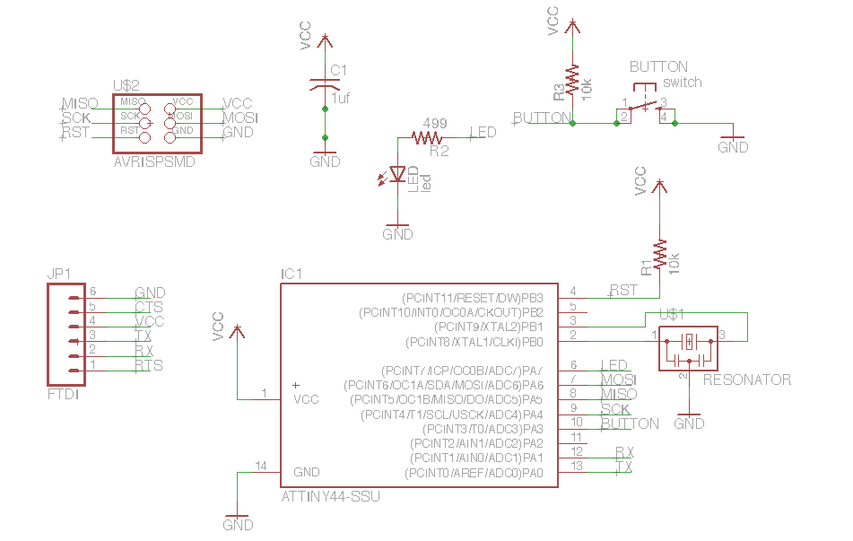
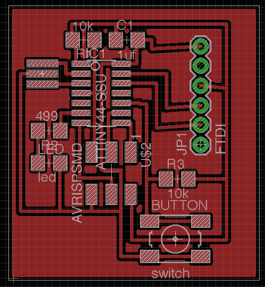
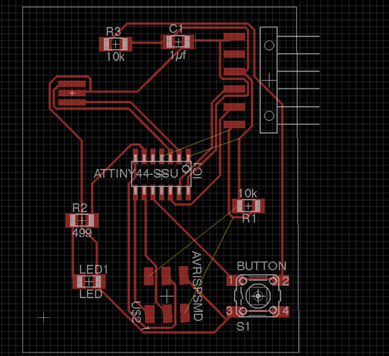
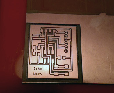
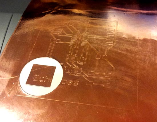
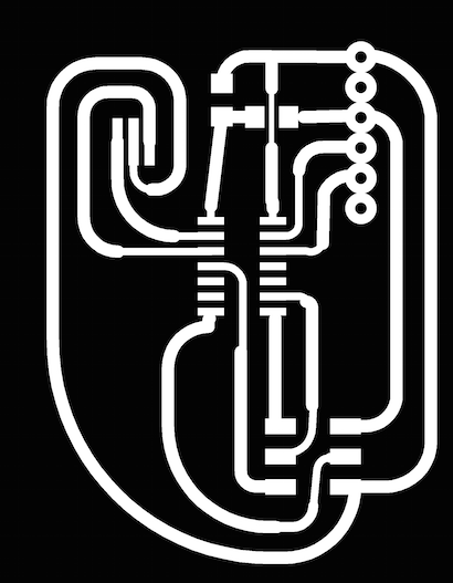
the final schematic and board layout
Things I found
- Do not press "drop" when adding components, you'll disable the active library ughhh. I thought this was meant to add component to the schematic. I'm not the only one, apparently.
- I had a hard time finding the right components sometimes. When I opened the original board I could right-click on a component and view its properties which gave me clues as to how to find it in the libraries.
- When naming the nets (they become invisible connections): first name them, then use the label command, click on the connection again twice and the name of the net will appear. It's easier to read it that way.
- I cleared up all mistakes with > Tools > ERC. But got stuck on: "Only one pin on net CTS". I couldn't find any info on it and quadruple checked my board with the examples so just decided to lose it. What's the use of having a net with nothing connected to it?
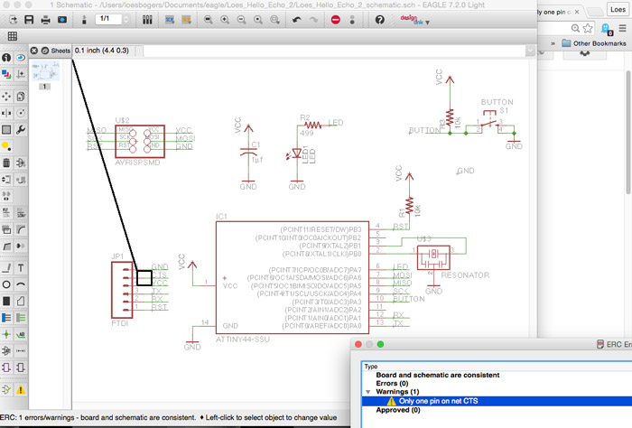
- Big mistake, it turned out: I thought there's a mistake in the naming on the FTDI: RTS should be RST (thats what all the other nets are called anyway). So I changed it, but when routing the board I saw all sorts of connections that weren't there in the examples. So at some point I changed it back to RTS. And the ERC of course told met that there was "only one pin connected to net RTS" and the CTS net mentioned above. Rather than deleting the names, I triple quadruple checked how the connections were running in the examples and decided to keep the names and just accept these errors because there was no reason for me to assume this would be a problem. It would just become a square to solder the leg to...? Right??? Fingers crossed on that. Routing became so much easier after that...
Impossible airwires, probably caused by me changing RTS to RST....and generating extra connections
- type "ripup;" command to unroute all autorouter traces in one go as I found here.
- when running the autorouter, I kept having some unconnected airwires. Some research told me that adding a 0Ω resistor could act as a bridge to cross over another trace. I didn't use this in the end, because I managed later on.
- It took me a while to find the Design Rules Document for the Roland Modela, first a found one that gave me a lot of errors, then I found this one that seemed to work better. Here it is the one listed here
- I made a version with a name on the board and and a ground plane (looks nice, saves milling?). Having the text gave a DRC error as well, which I accepted because it doesn't influence the circuit. But of course later on it didn't cut properly.
- I made a screenshot of a board overview with component names and positioning, of the schematic, and I exported a parts list for each design. Easy for later. Find them all in the zip file below.
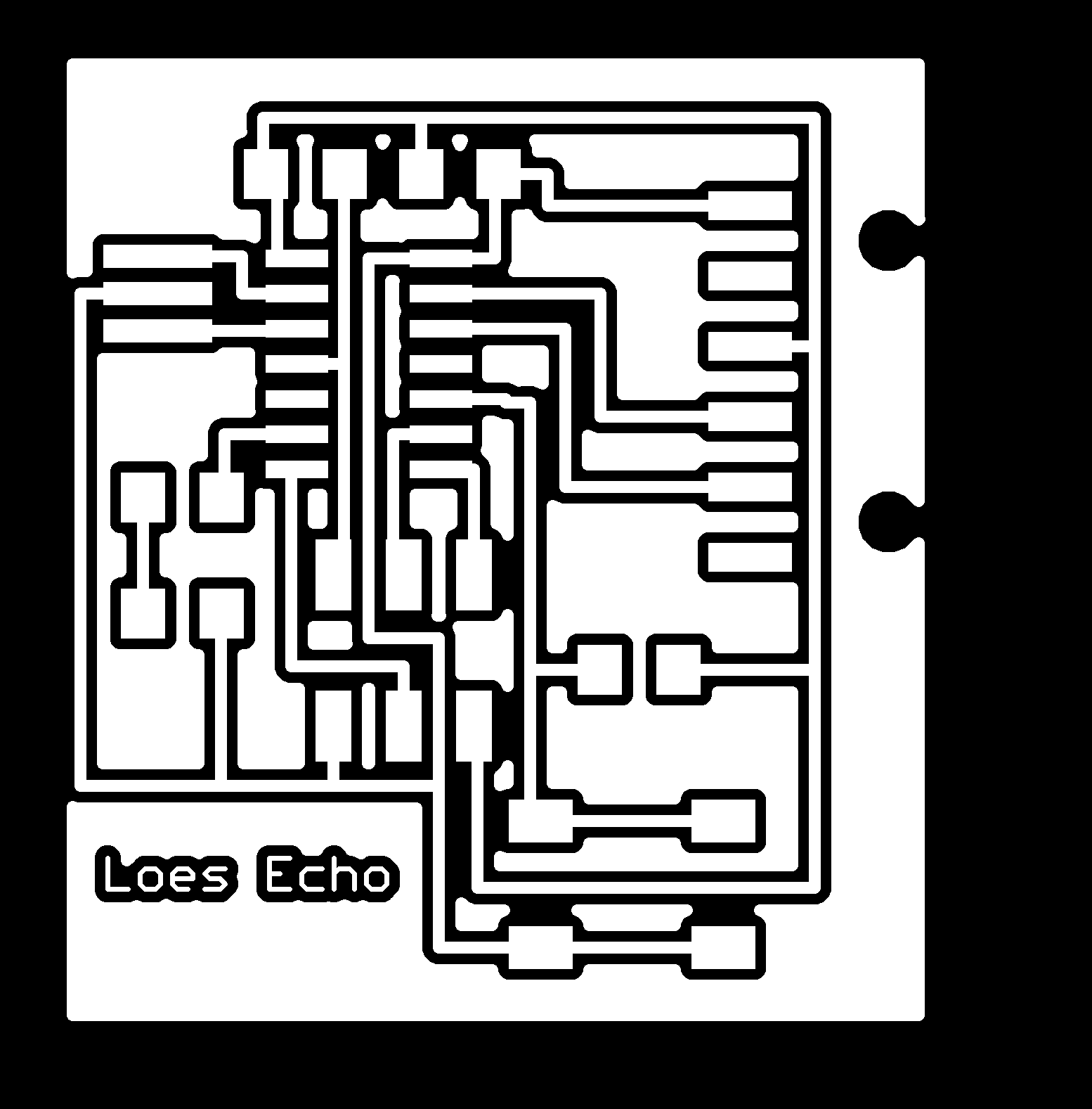
the traces for the board with a ground plane
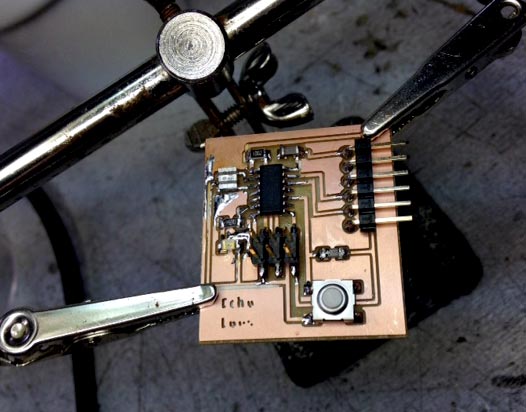
Milling and stuffing the board
For the milling I followed the steps as documented in the Electronics Production week . I used these settings:
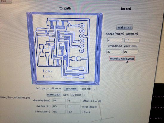
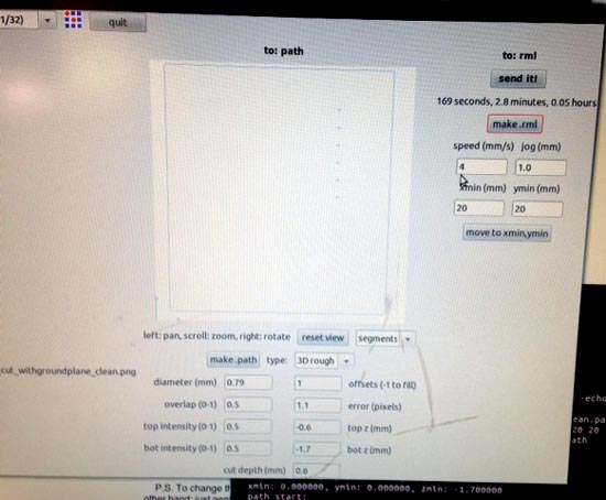
The settings for the modela
- I had to replace the FTDI for a surface mount one from sparkfun. I downloaded and installed the "sparkfun connectors" library for it, put it in without nets, checked if it was the same size as the previous connector, and then replaced it with the replace command
- my name didn't mill so well I guess the letters have to be even bigger still. I did it in Gimp but should have scaled it up.
- the lowest trace on the bottom left is really thin but I checked all connections and they work fine.
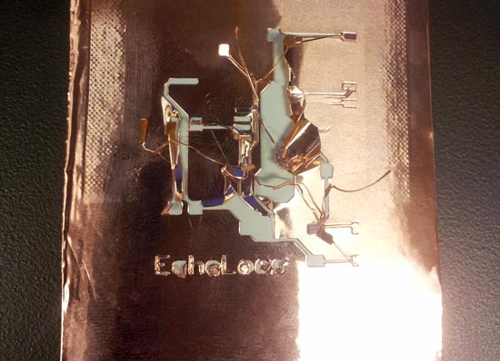
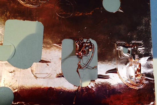
- I milled the board with the ground plane. Before I sent it to the machine I cleaned off some fiddly bits around the IC to make sure the traces are clean around the little legs.
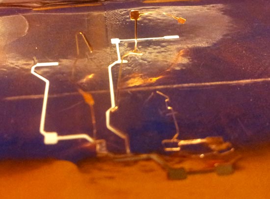
- Stuffing went alright, I had to look up whether some parts had an orientation but now know what to look for in the datasheet. Usually they mention drawings indicating GND or cathode if they have an orientation
- I didn't have the best soldering day (shaky hands). There's some solder spills so it doesn't look super but it does the job.
- resonator trick by Casper: solder the three lines, then hold the component steady on top while heating it with the heat gun until it sinks. Top job.
- next time I'll give the board rounded corners, feels a lot nicer in your hands (especially when washing the board haha)
Workfiles
- final milling files
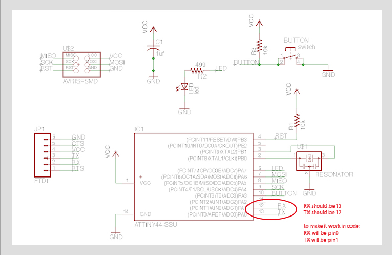
Update from the future: mistake in schematic!
in the programming week I noticed a mistake in the schematic, see below and check out the documentation of week 07 to read more
Design for the Vinylcutter
I was intrigued by the idea of making flexible circuits so used this week's assignment to try it out. I used these resources to find out how and what:
- this fab tutorial. The link to the custom dru was broken but I retrieved it via Waybackmachine. This is the dru file again
- this one by astrid lubsen
- and this one on how to operate the machine
I didn't find a whole lot of information on what design requirements to follow for Vinylcutter circuits, except this guy mentions that 1 mm traces worked for him. So I tried it. So to keep in mind, tips by Neil and read in resources:
- Set design rules for vinylcutting (see dru file above) in > Edit > Design Rules
- make round curves (easier for the machine that straight corners)
- make 1 mm(!) wide traces. Note that ICs and small legs will be very difficult to do
- set the Net Classes before autorouting: set all to 1mm (found under > Edit > Net Classes
- reinforce connectors with gluegun after soldering
- make sure copper foil is not crumpled
- put copper foil in the middle of machine: edge is more straight there
- send cutting job via illustrator
- test to find right force and speed
- when foil flies up while cutting, pause it, press it back
- draw extra squares for easier weeding
- weed it from the backing
When I finally found the right dru file I could easily do a DRC check and autotrace the board. Saved only top layer as png, and ready to roll!
Fail fail and fail some more :)
So the whole vinyl thingy didn't work out in the end, here's how it went down...
- attempt 0: 20cm p/s and force 150gf was a trainwreck. Cees suggested I try this too because he uses these settings usually for vinyl. I was sceptical but always willing to try...
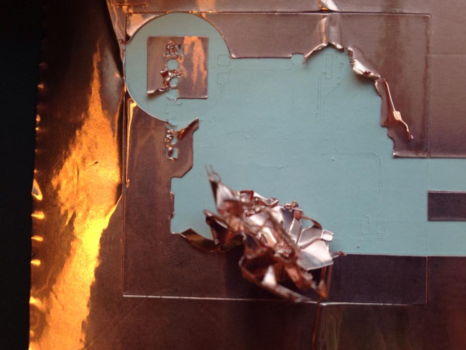
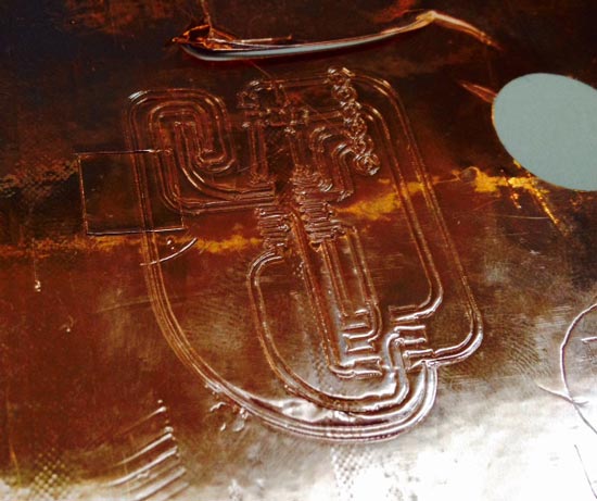
- attempt 1: 1 cm/s and 45gf: did not go through. But was a pretty picture
- attempt 2: 2 cm/s and force 100gf: perfect test, terrible circuit, traces were flying through the air.
- attempt 3: 1 cm/s and 80 gf, didn't go all the way through.
- attempt 4: 1 cm/s and 100 gf, traces flying in the air...Beautiful result though I wish I could cast it in silver and I would wear it like a broche.
- this was when I started considering changing my drawing, however this circuit is quite and routing with 1mm traces only gave max 45% succes with autorouting, 0.8mm which I was willing to try only 62% so I decided it wasn't going to happen this week. I still had to mill my board. First things first.
Some conclusions about PCB production with the vinyl cutter
The settings listed in other people's documentation (1-2cm/s and 40-50gf) were way off compared to what worked for me. It didn't even go through at those low settings, I was looking more at the 80-100gf range. I now did find a way to control the thickness of the autorouter settings which is super useful if I'll try again in the future. (Edit > Net Classes). I will for sure try this again with simpler circuits, eg. led strings etc. The teeny tiny legs of the microcontroller made it almost impossible to route the traces with a thickness and clearance of 1 mm.
The last thing I tried was to redraw it AGAIN. I got rid of the button and the LED for the purpose of the exercise. Added a 0ohm resistor bridge (this resulted in an airwire but ok). And I rerouted all traces with 1mm, except where the clearance became a risk, there I had bits of 0.6 or 0.8mm but kept to a minimum. This will be my last shot at fame...here goes nothing.
No successes later on either. I tried loads of settings, high low, fast, slow, everything. Cut on the left of the machine, cut on the right. Did multiple runs on the same route. Not of it worked. Either it didn't cut through or it flew up and wrecked the circuit. Zaerc is looking up his documentation to see how he did his successful vinylcuts and I'll take it from there..
Workfiles vinylcutter
- the vinyltraces that didn't work
- and more vinyltraces that didn't work
- And the last results....
