Rotogravure Printing PCB
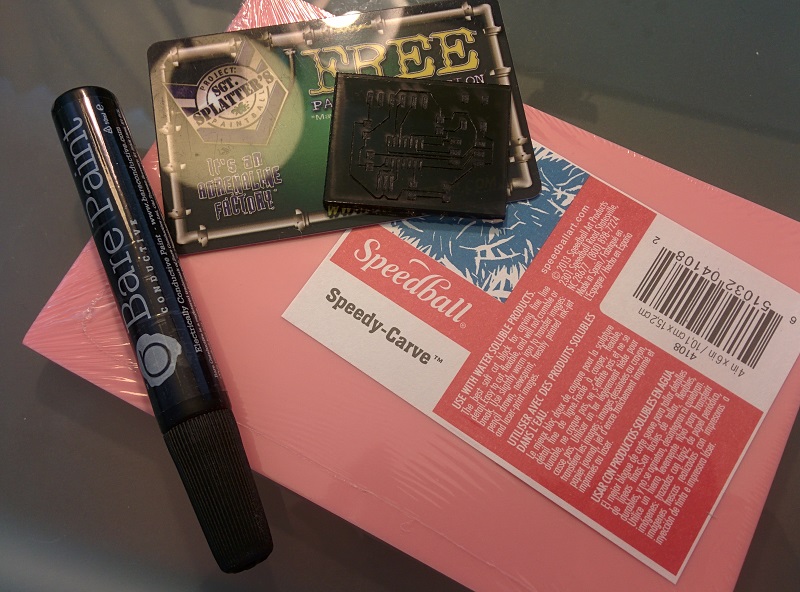
Basic Equipment: stamp rubber, laser etched acrylic with PCB traces, conductive ink/pain/glue, something that can be used as squeegee to wipe off excessive ink/pain/glue.
 First, I laser etched the PCB traces onto a piece of acrylic. It's about 1mm deep.
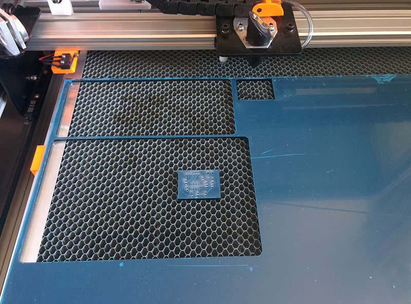
First, I laser etched the PCB traces onto a piece of acrylic. It's about 1mm deep.
I use Bare Paint Conductive paint since that's what I have on hand.
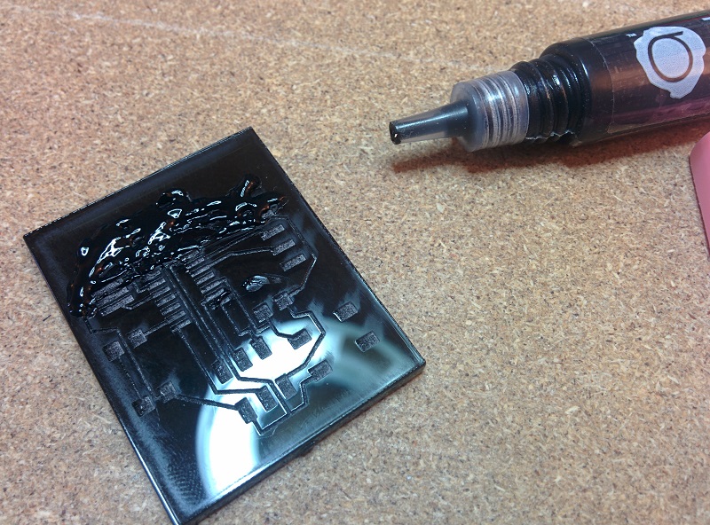 And use a plastic card as the squeegee to wipe out the exessive pint.
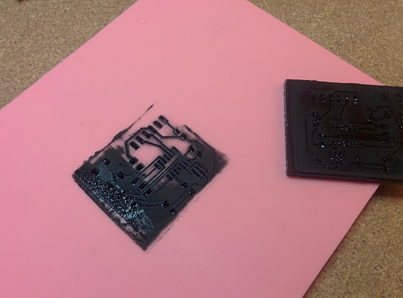
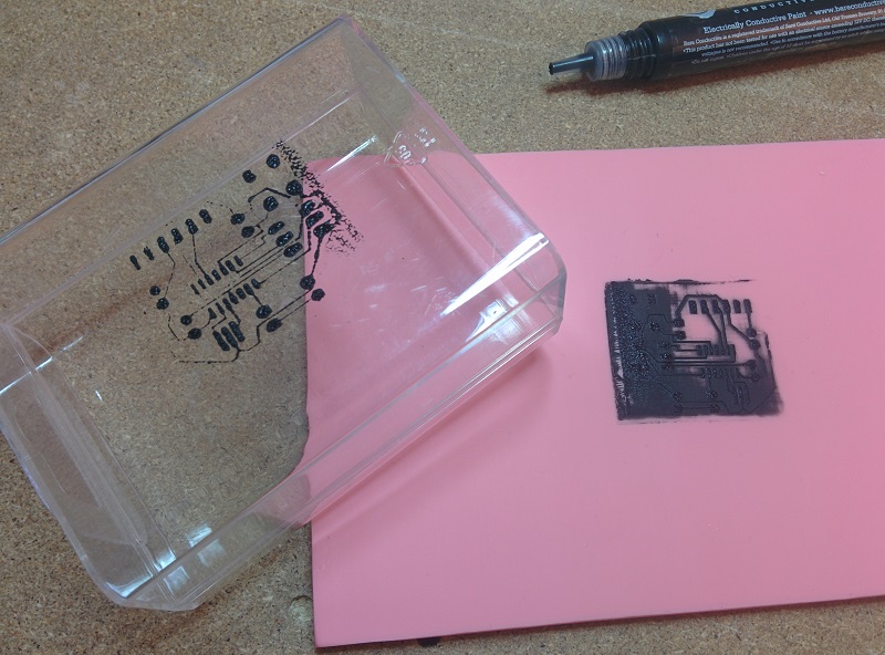
 With only paint left in the traces on acrylic, I used the stamp rubber to transfer the PCB trace shaped paint onto a piece of clear plastic (in theory, can be any surface that's not conductive). The transfer process is to simply press the stamp rubber onto the paint filled acrylic to collect the paint, and use the same stamp rubber to stamp onto a surface of ur choice.
And use a plastic card as the squeegee to wipe out the exessive pint.
With only paint left in the traces on acrylic, I used the stamp rubber to transfer the PCB trace shaped paint onto a piece of clear plastic (in theory, can be any surface that's not conductive). The transfer process is to simply press the stamp rubber onto the paint filled acrylic to collect the paint, and use the same stamp rubber to stamp onto a surface of ur choice.
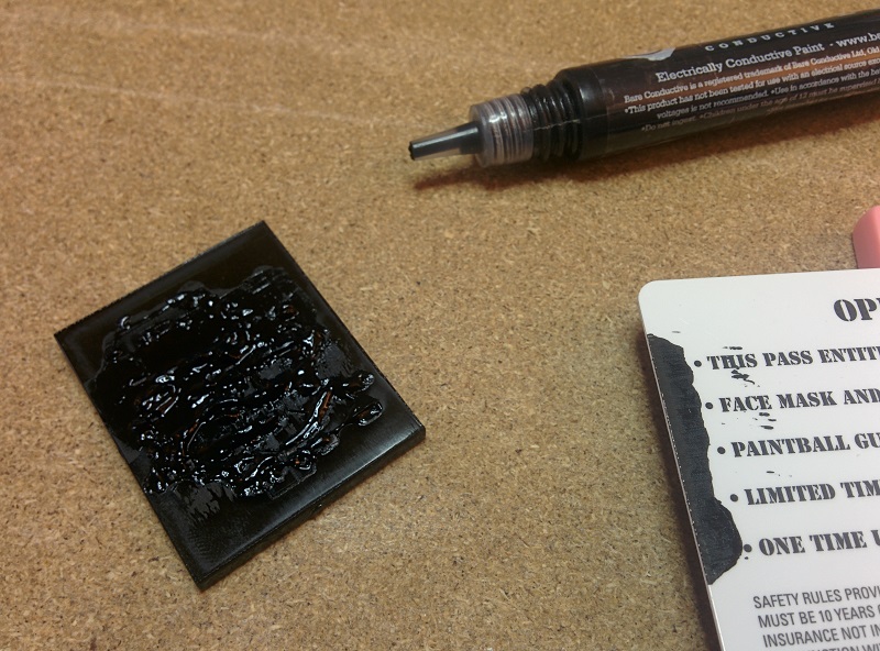
 Even worse, the resistance of the traces that has been successfully transfered and dried are really high. Mostly due to how thine my traces are.
 The experiment is far from successful, but I do have some ideas that might improve the result.
First, make the traces wider and also laser etch the traces deeper, so there are more paint to form the traces, hence lower resistance. Secondly, try other pain. Since the process was successfully used with nail lacquer, I'm thinking about mixing graphite powder with clear nail lacquer to form a new conductive paint to try.
The experiment is far from successful, but I do have some ideas that might improve the result.
First, make the traces wider and also laser etch the traces deeper, so there are more paint to form the traces, hence lower resistance. Secondly, try other pain. Since the process was successfully used with nail lacquer, I'm thinking about mixing graphite powder with clear nail lacquer to form a new conductive paint to try.
 That's it for now, at least untill I receive my graphite powder and steel shim.