
Assignment Week6
Electronics Design
This week’s assignment is “redraw the echo hello-world board,
add a button and LED check the design rules, and make it"
I try to make it and adding switch and LED.
Using EAGLE Schematic Editor
I have already installed EAGLE.
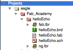
So first, I download “helloEcho” circuit data.
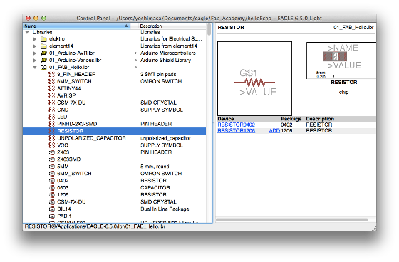
library file move to EAGLE lib folder.Then, I can find some device about Fab Academy assignment.
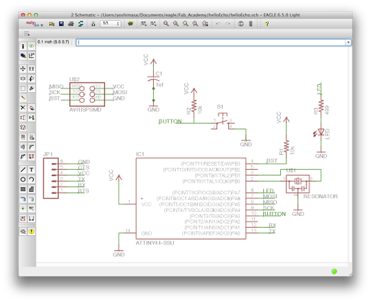
Next, I opened EAGLE schematic file “helloEcho.sch”. And added switch and LED. Switch and LED found in “fab.lbr” library.
To attach icons of devices in EAGLE schematic, selected and cricked text “ADD” in neighbor frame
By the way The number “1206” is explain size of parts. “1206” is 3.2mm x 1.6mm.
Then, when mouse cursor put on schematic window, I could see moving icons of devices.
Line tool can connect between icons and icons. If you complete this process, next, we have to check “net”.
The “net”explain connection between parts and parts.
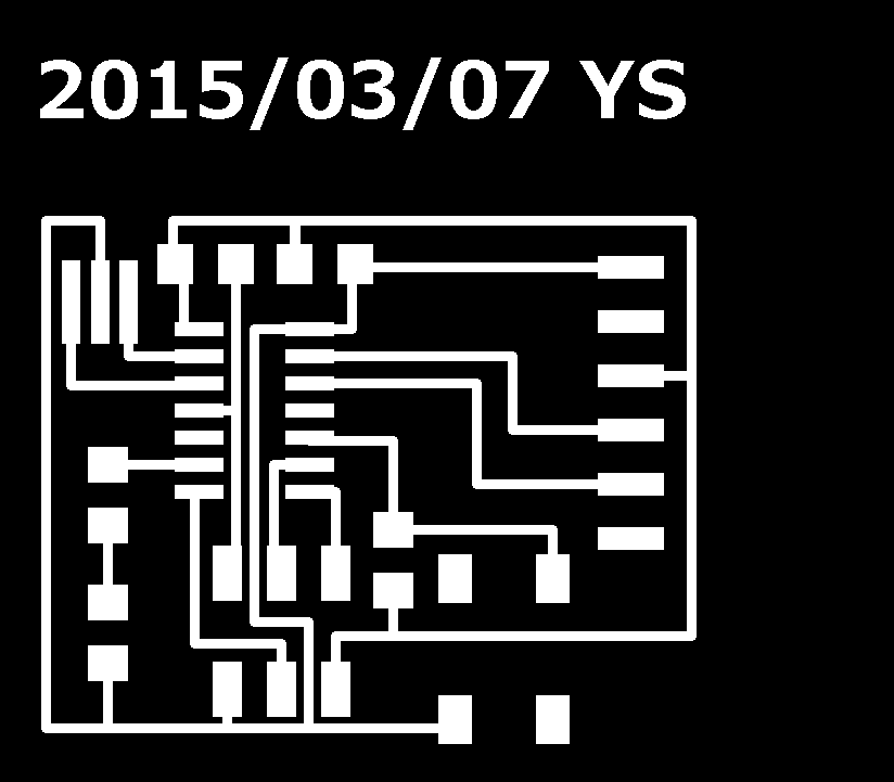
Using EAGLE Board Editor
If we finish edit the circuit schematic, next, have to edit board pattern.

This window can edit parts layout. parts can't put out of board area. And, can't layout parts that cross pattern. Circuit pattern line can draw "Route" tool. Board area can edit. Select "info" tool and click on white line of PCB outward form.
Then the info window of outward form appear, so we can see Coordinate numbers of outward form.
So we can edit PCB outward form.
If we complete editting board pattern, next, make .png data of circuit pattern and outward form.
Select "layer setting...". and appear layer window.
To make circuit pattern, display only "Top" layer, and export "image".
To make outward pattern, display only "Top" layer, and export "image".
Milling PCB
.
I mill PCB board using MDX-20 and Fab Module. The config of Fab Module is same. But I had trouble. When I was milling PCB, the end mill was broken, and PCB's surface had very dirty burr. I didn't know why that burr was made.
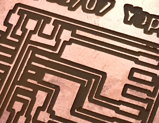 Very dirty surface. Circuit pattern was broken.
I was given some advices from instructor Take. He recommended to edit Fab Module's config of circuit pattern.
So I edit parameter and try make.path. Then preview picture of path become more straight and beautiful. I find that Fab module's config is very important for milling. quallity.
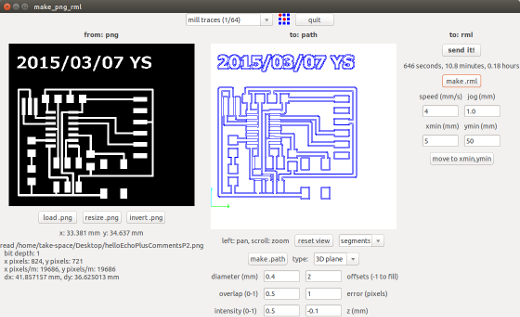
 Berore editting parameter. The preview of circuit pattern is not straight line.
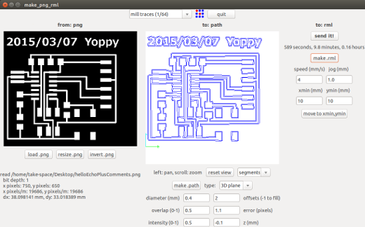
 After editting parameter. The preview of circuit pattern is straight line and beautiful.
The difference of condition is number of Fab module's parameter "error(pixels)".
I don't know why the parameter is make difference, but I find this parameter is important to mill PCB.
I inform Take and other member of FABLAB Hamamatsu.
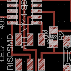
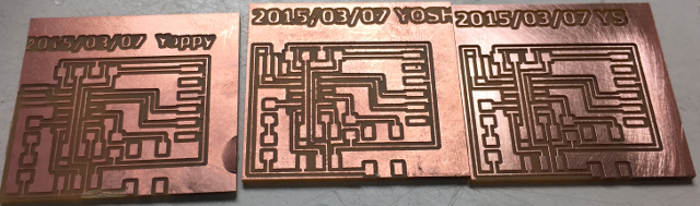 Left and center PCB is fail version.Right PCB is success version.
Circuit pattern data can download here.
Circuit board data can download here.
There are Eagle data. sch and brd.
I soldering electric devices, and check the connection using tester.
 Complete !