- Logged in as: fablabtaipei (fablabtaipei)
- Recent changes
- Media Manager
- Sitemap
- Admin
- User page
- Update Profile
- Logout
User Tools
- Logged in as: fablabtaipei (fablabtaipei)
- Admin
- User page
- Update Profile
- Logout
Site Tools
Table of Contents
Electronics Design
MultiSIM Blue
 First I tried MultiSIM Blue. Because my laptop is a MacBook Pro, I installed the latest Parallels (14 day trails) and create an instance of Windows 10 Technical Preview. MultiSIM runs fine on this latest version of Windows. However, the GUI looks a little old-fashioned to be and the icons are really small on my retina screen. It was not fixed even if I magnified the font size on OS, so I gave it up.
Fritzing
Schematic
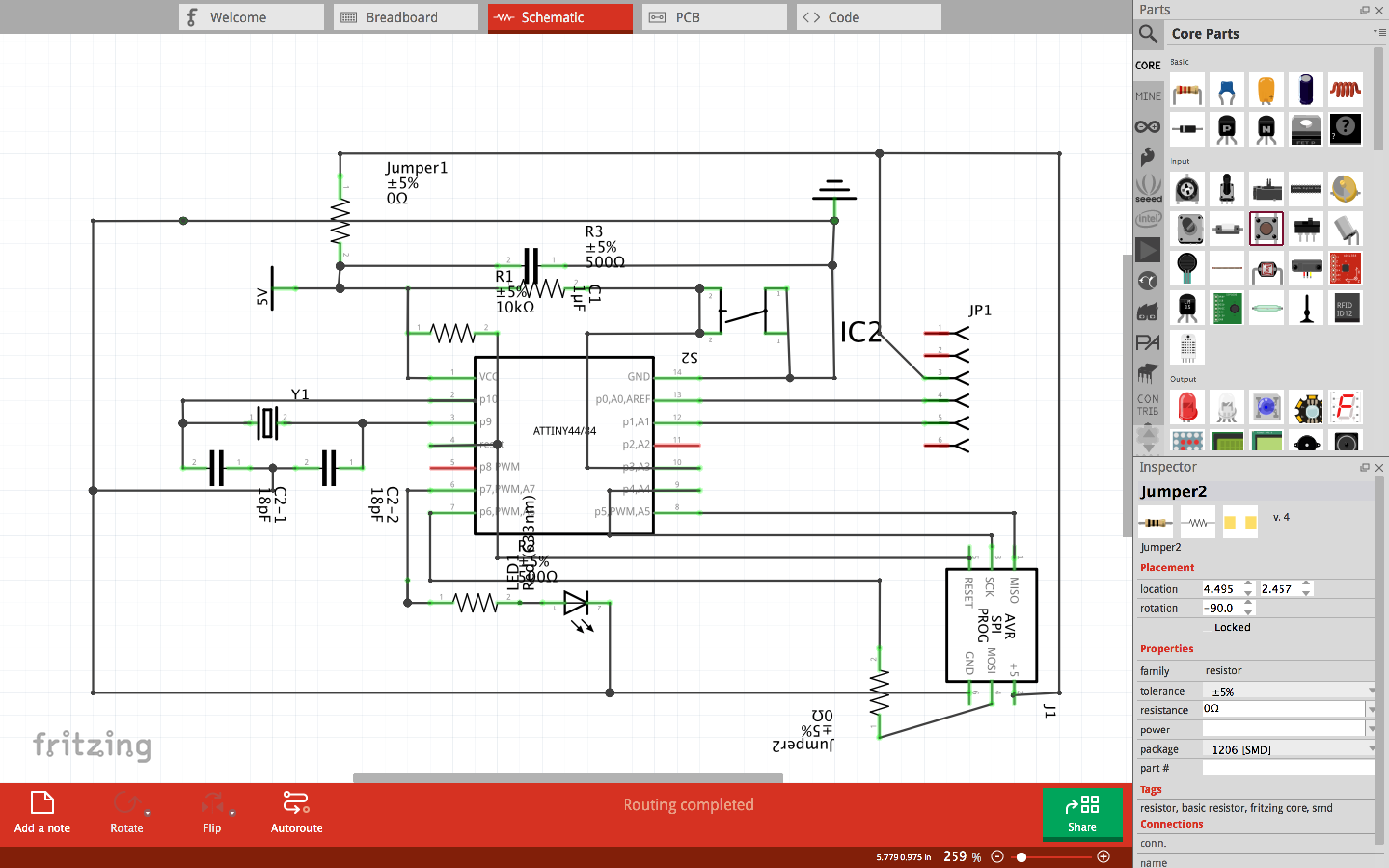 Then I jumped to Fritzing. I love the style of its GUI and I don't need any tutorial to hand on it. I searched for the components very easily with the Parts panel, except for Attiny44, which is not in the library. Fortunately Fritzing allows creating your own parts and adding to your parts collection. I found exactly what I need on The Project Inventory. Making schematic in Fritzing by drag-and-drop is easy. Laying wires is very straight-forward, too. After a couple of fun hours, I got the following.
PCB
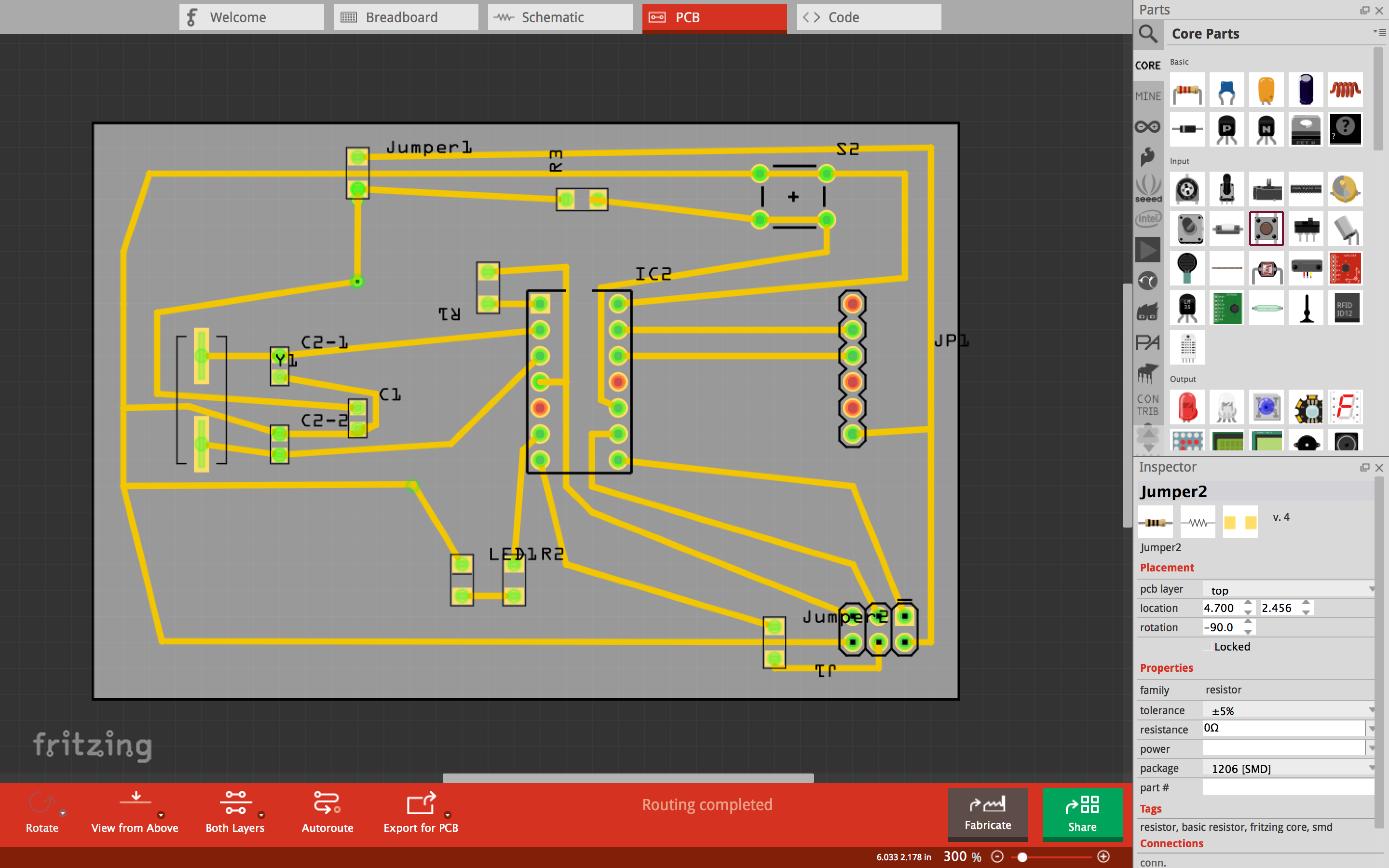 Switch to PCB tab. It was a mess because all the parts are randomly displayed (looks so.) Before clicked on auto-routing, I rearranged the parts to be like what I did in schematic (Otherwise routing is definitely in vain). I was confused why I had to lay my parts again. It turned out that I did not have to put everything in one piece in schematic, but early efforts were not in vain because I could repeat the layout. Finally I auto-routed it and changed some wires to avoid shorts. Two things to note: one is that Fritzing always route it in two layers: top and bottom. It will put the wires to the bottom layer when there are unwanted intersections. In my case, I wanted wires to be only in one layer, so I remove all the intersections and put all the wires to the top layer. The second thing is jumpers won't find the right places. I had to carefully arrange the position of jumpers to let the wires go under them.
Export
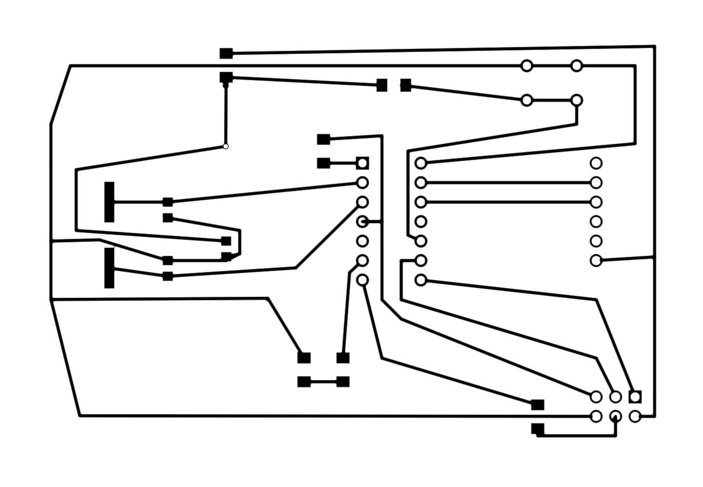 Completing my layouts, I exported it in pdf format. At first I exported to svg format and fed it to fab module, but fab module seemed to treat the file for laster cutting rather than electronics production. Therefore I used pdf format instead and converted it to png file. The image should be inverted in color (the lines should be white and the background should be white.) but I found that fab module could do the job for me.
Enhancement
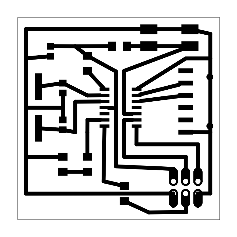 The first version of my PCB is 8 cm by 5 cm with much space between parts and wires. Therefore I made s second version with a compact, 4.2cm square layout. I also replace the through-hole parts with SMD parts (appears as squares, not circles.) To choose amount SMD parts, check the top three icons on the property window after click on it.
 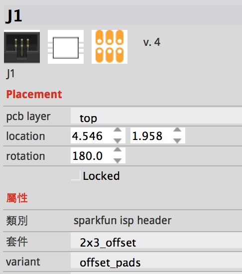 The center one shows what it appears in schematic and the right one shows what it appears in PCB.
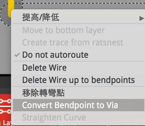
Another tip is lay the bendpoints with parameters. This was not possible before converting the bendpoints into via by right-click on them. After the vias are set in the right positions, right-click on the again and convert them back into bendpoints, because vias has a hole that we don't want on PCB.
You may download the file week6.fzz.
Production
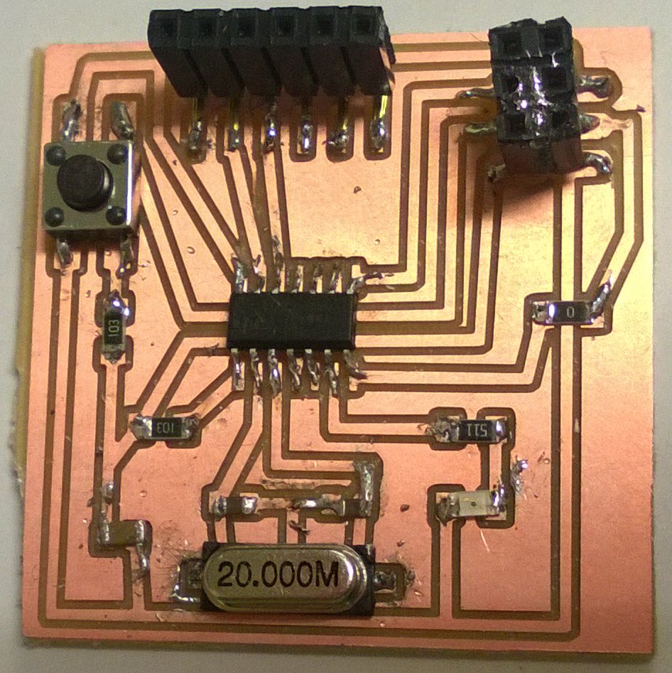 Finally put it into production. I use Roland Modela MDX-20 and the default setting with some minor changes. I drill two traces instead of four to cut half the production time. When cutting out the board, I set the depth with 2mm. Then I solder the parts onto it.