week 4. Electronics prodiction
What are we about to do here?
|
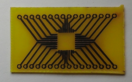
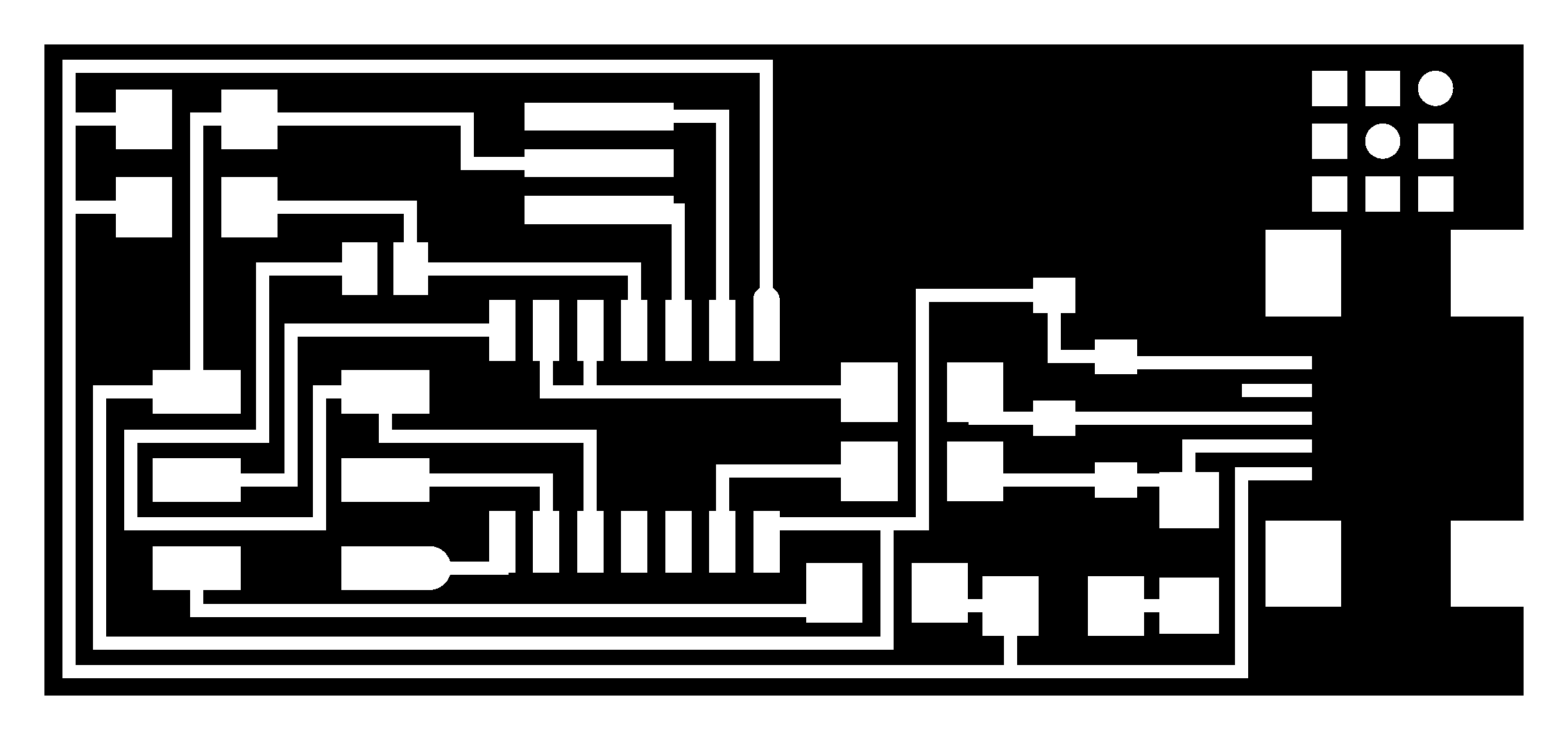
Our assignment for fourth week is to make the Fab_ISP in-circuit programmer. We already have the outline in png-file (you may see it on the right) and all we need to do is to turn it somehow into the instructions for modella and then send it there. There are few ways to each of this steps. Let's see what's that all about!
The right way to make our pcb...
... is to use fabmodiles and be happy. It is really nice way, but first I thought that it needs either to run ubuntu or MacOS on your computer or to compile it in cygwin. And what if you dont have any of them at the moment and it is difficult for you to build fabmodules from source code?
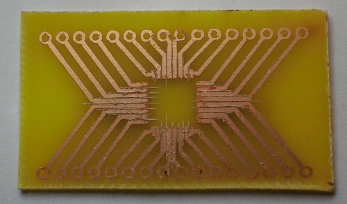
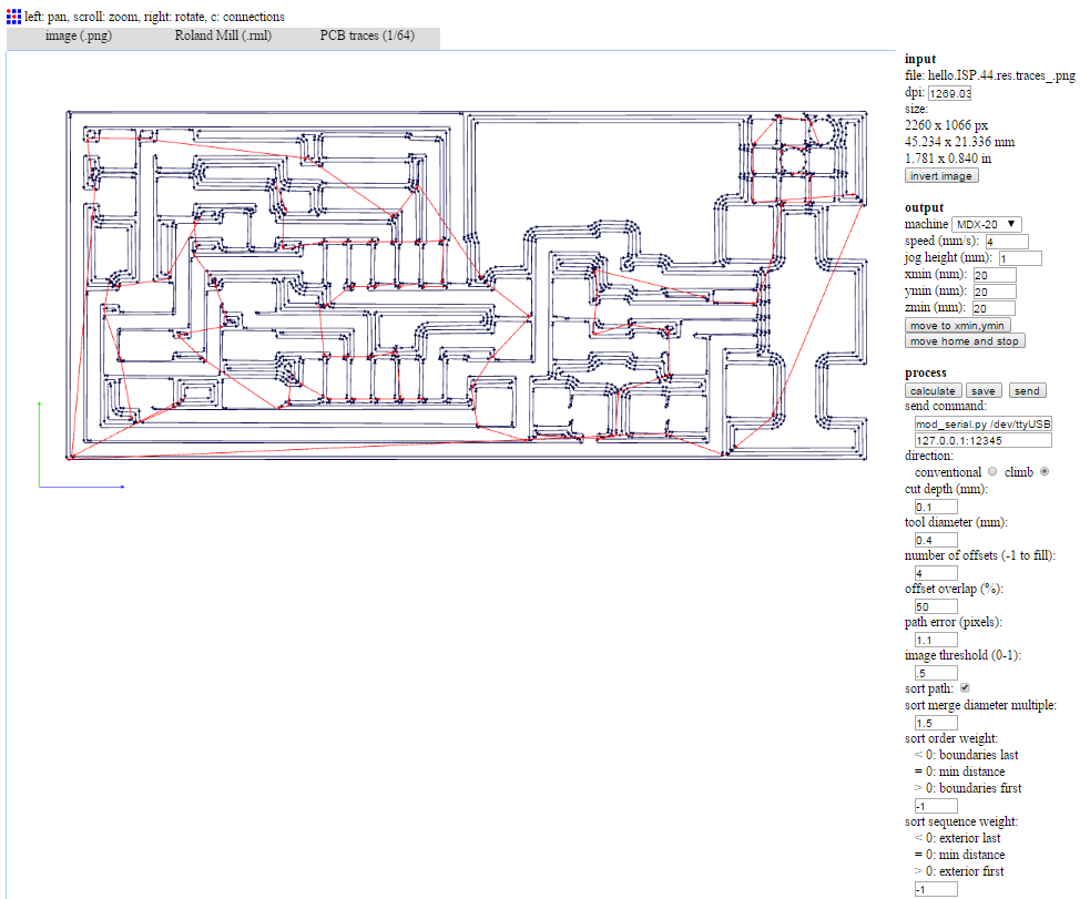
Luckily we can use the online version of fabmodules (you can find it here). Here we need to pass through several steps (When we're done, we shall have the nice pcb, just like mine on the right):
|
|
Luckily we can use the online version of fabmodules (you can find it here). Here we need to pass through several steps:
choose the input file
choose the output format
choose the way you want your pcb to be processed (A little more about that below)
Set any other parameters you would like to change.
send it to modella or export to *.rml if you have problems with access to the com-port from browser. If so, you can send your rml-file (let's call it out.rml) to port straight from comand line using comand "type out.rml > com1". I got this information from here.
If you have tool thin enough to make this pcb (it was designed to be milled with quite thin tool any thicker thnn 0,4 mm will give us a mess during the calculation. I'll show that below), then it is ok to choose the parameters shown on the screenshot below
The tricky way. What problems did I face?
First, I didn't have any tool thinner than 0,5 mm. Let's see what do we get if I change tool diameter to 0,5 mm:
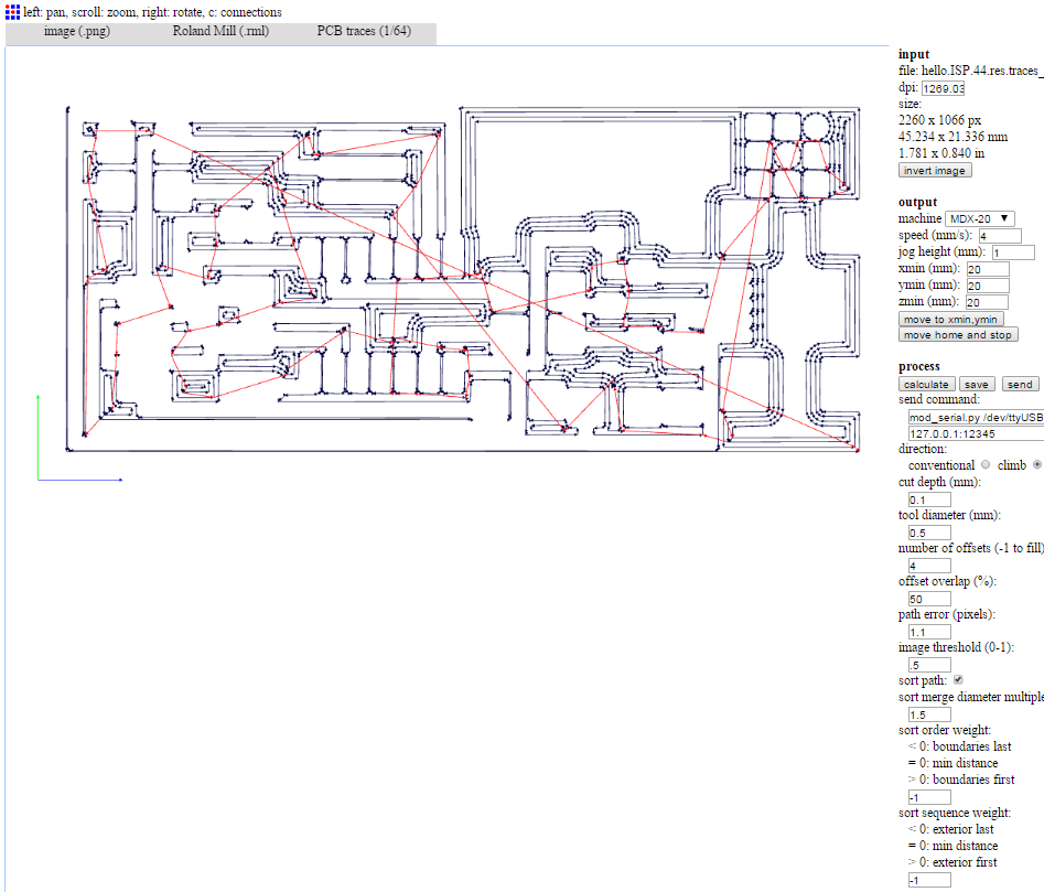
As you see, the traces at the place of usb-jack are connected. What can we do in such a tricky situation? The problem can be solved (I milled my pcb with 0,5 mm tool). To solve that we need to convert our png file to svg and then edit it in inkscape or corel draw (I made some extra contouring to encrease the traces thickness, then exported it to *.dxf and imported into dr.engrave - modella native printing agent). That is not as cool as using fabmodules, but it gives the result.
More illustrations for this process can be found here
Are there any other ways?
To be honest I didn't play with fabmodules for long enough to make sure, that there is no any other way to make this pcb with thicker tool without quality loss. Maybe there is.
We could also redraw the pcb in eagle (or some other cad) and export another png but this is beyond this week assignment. What's not is fabricating, soldering and flashing the FAB-ISP
Soldering and flashing
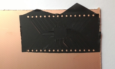
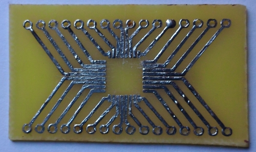
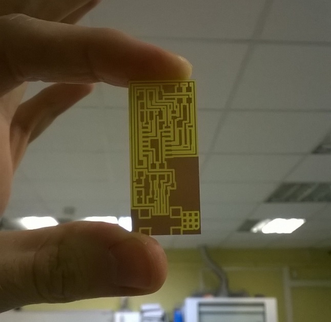
After all those tricks I told about before I suceeded to mill the FAB-ISP board:
Then I soldered it:

Half-soldered board
|
Soldered completely, not flashed yet.
|
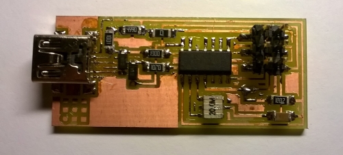
Then I flashed it and now I use it for flashing other boards:

Some uncommon technologies for PCB fabrication
Why on earth not to mill?...
The answer is very simple - we were out of tools for modella! I mean out of really nice thin tools you could mill everything good with. So I started looking for alternative ways to fabricate the PCBs and one of them is etching. I know that etching is really nasty, that's why I am working on the recycling process right now not to depend on anyone else
Disclaimer!
The data below does not pretend to be absolutely correct. It is author's opinion about this subject based on his personal experience and may contain some factual errors. Thus any technology described below should be used by anyone only at one's own risk and the author assumes no responsibility for any consequences of using the described technology.
But still, my concern was to make it all as fair as it can be.
Safety and accident prevention.
Working with chemicals may be a little bit dangerous if you are unprepared, so what you need to know is:
Ferric Chloride (Iron(III chloride) is slightly toxic, so to work with it you may need to use personal protective equipment such as: gloves, respirators, protective glasses.
If the ferric chloride gets on your skin, rinse it immediately in running water with soap.
If the ferric chloride gets into your eyes, rinse immediately in running water.
During the copper etching process the solution may become warm and thus some amount of chlorine gas may be released (but not necessery will because the reaction depends on solution temperature). Anyway, good ventilation is highly recemmended.
CuCl, which is the product of the copper etching reaction is a toxic waste and should not be poured into water-piping. Thus, it has to be utilized.
Speaking of etching
Etching is the process of using strong acid or mordant to cut into the unprotected parts of metal to create relief in metal and is, along with engraving, widely used in printmaking today. In our case etching is used to remove the copper filling from FR4 to shape the pcb-outline.
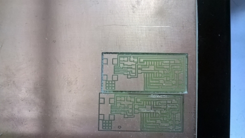
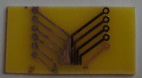
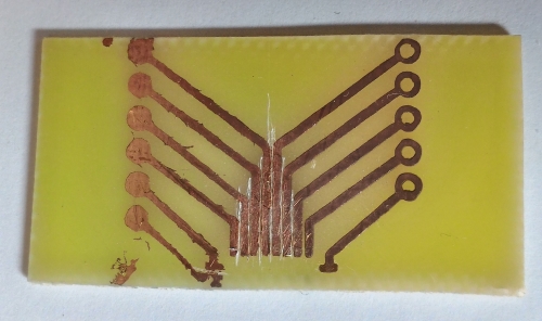
The result is something like this (on this picture you may see the etched traces covered vith vinyl protection on the left and without it on the right):
A bit of a chemistry and a key to recycling
The equations for this process (which is going through two stages) are:
FeCl3 + Cu → FeCl2 + CuCl;
FeCl3 + CuCl → FeCl2 + CuCl2.
That's the straight direction for the process. The question is: can we revert it? What if we add some iron nails to the solution?
CuCl2 + Fe → FeCl2 + Cu
Not bad... We could try to remove the copper precipitate by filtration (Hey, we've got some copper!) and then to activate the solution with hydrogen peroxide or with passing the oxygene (just air compressor and a tube) through it. This technology is more in theory than in practice right now, but I would really like to implement it during the rest of the summer and more than this - to provide the process (if needed) with fabricatable equipment to make sure it's really safe for user!
Technology, at last
Vinyls masks
Using vinyl positive
Using vinyl negative
Vynil positive/negative protector(left part of this PCB is protected with nail polish through the vinyl negative mask, right is just vinyl positive mask):
The left picture is before vinyl and nail polish removal, the right is after removal.
laser-cutting the outline
TBD
What's next?
More etching here is TBD.
Back to my assignments-list
Back to my main page