
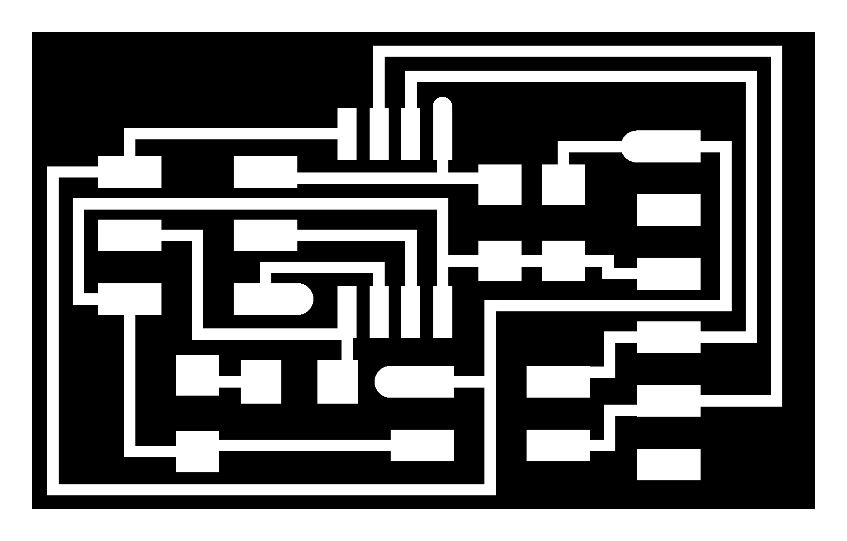
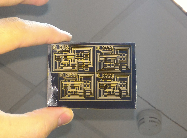
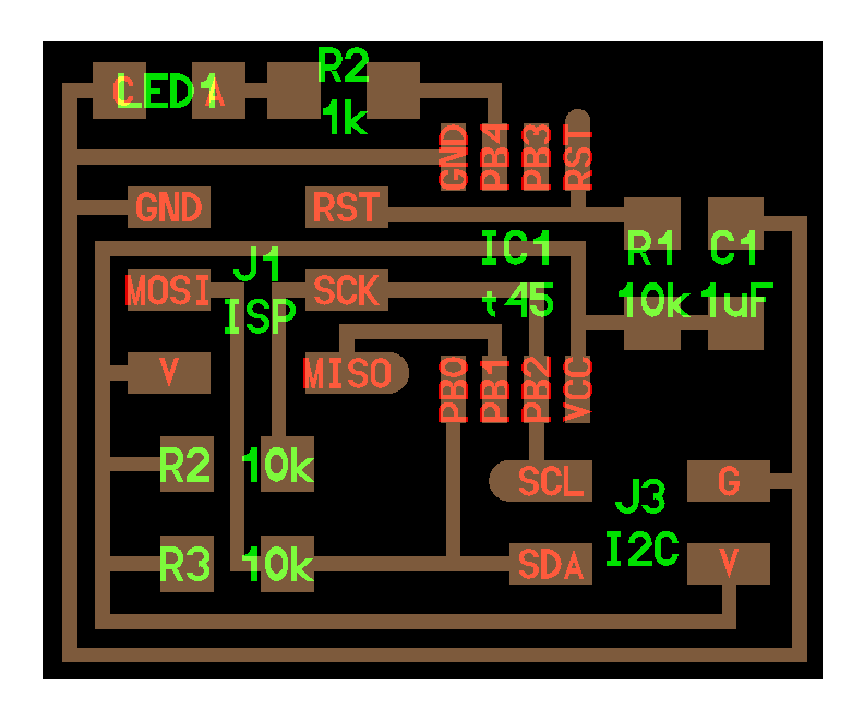
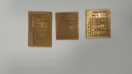
hello.bus.45.bridge board
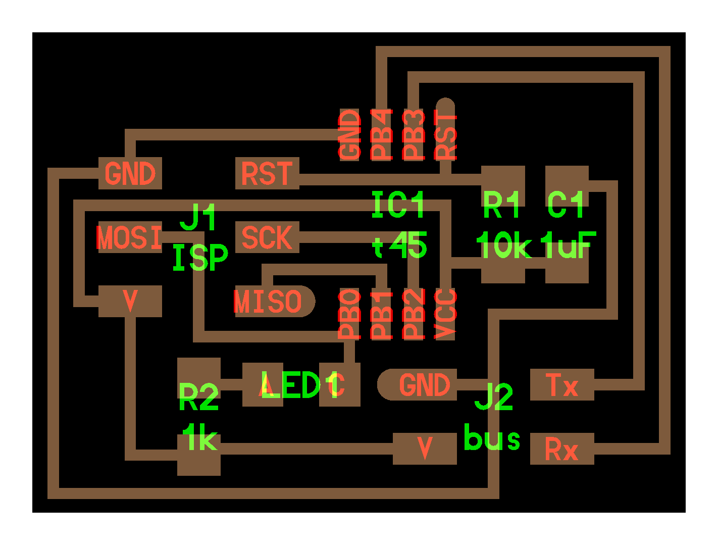
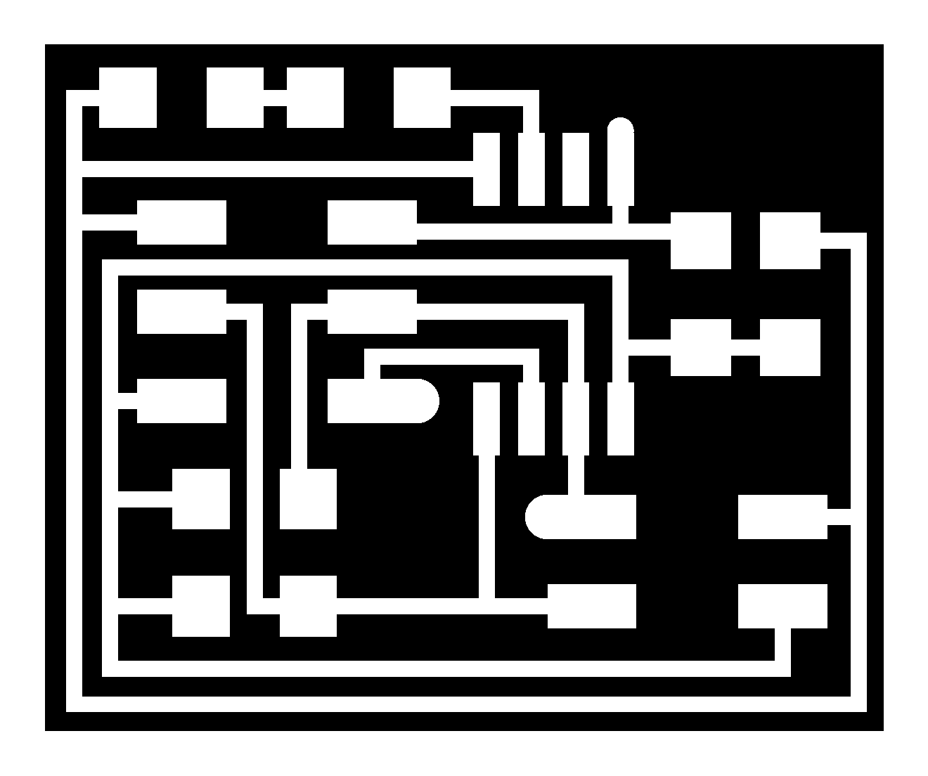
hello.bus.45.bridge traces

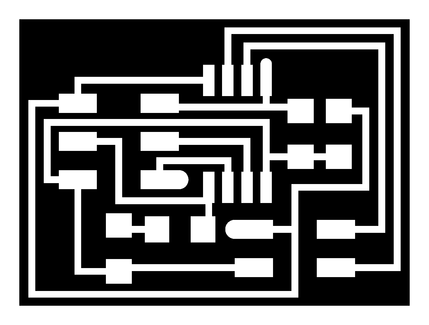
hello.bus.45.bridge interrior
Our assignment for this week was to "design and build a wired and/or wireless network connecting at least two processors". I decided to start from fabricating the all the example boards for serial communication because the more I practice the better my skills are and it is always good to begin from something simple with example c-dode (like hello.bus.45.bridge and hello.bus.45.node boards).
At the same time playing with hello.I2C.45.bridge board with two hello.I2C.45.node boards could bring me closer to understanfing the way to make SPI-communication using tiny-TWI. I want to learn SPI communacation to play with wireless communication using nrf24l01-based modules and that is what I wanted to use in my first final project proposal.
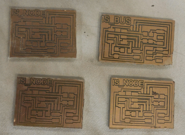
Here are the board, traces and interrior from networking and communications
|
hello.bus.45.bridge board |
hello.bus.45.bridge traces |
hello.bus.45.bridge interrior |
hello.bus.45.node board |
hello.bus.45.node traces |

hello.I2C.45.node interrior |
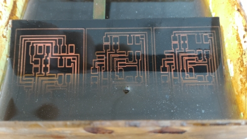
I made those boards with laser-etching technique. I described all the steps in details for hello.I2C boards below. I just added a signature to tell them from the other boards. Here are some pictures from fabrication process for this board:
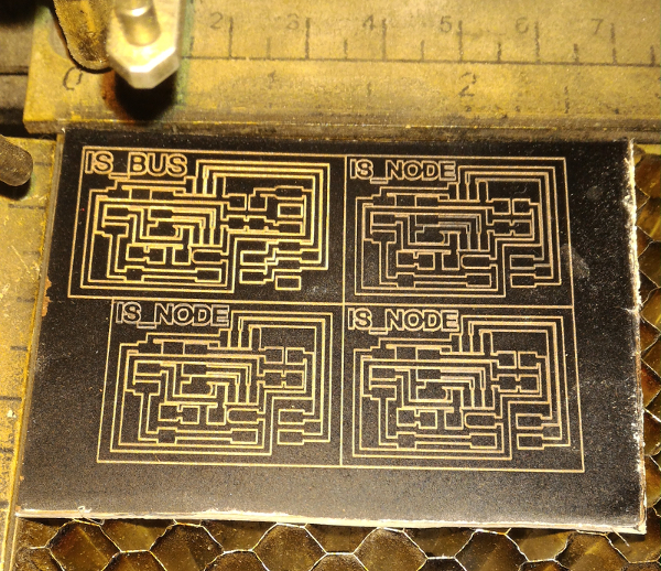
That is the board with laser-cutted paintspray-traces in our epilog laser.
The same after etching.
after the paintspray removal.
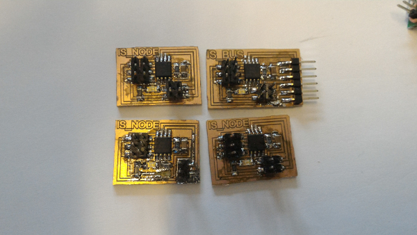
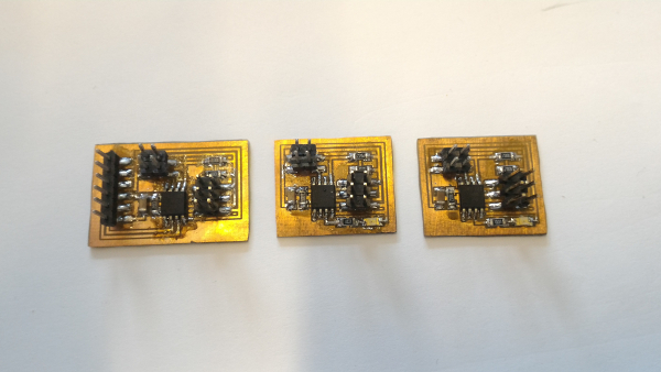
The boards are soldered!
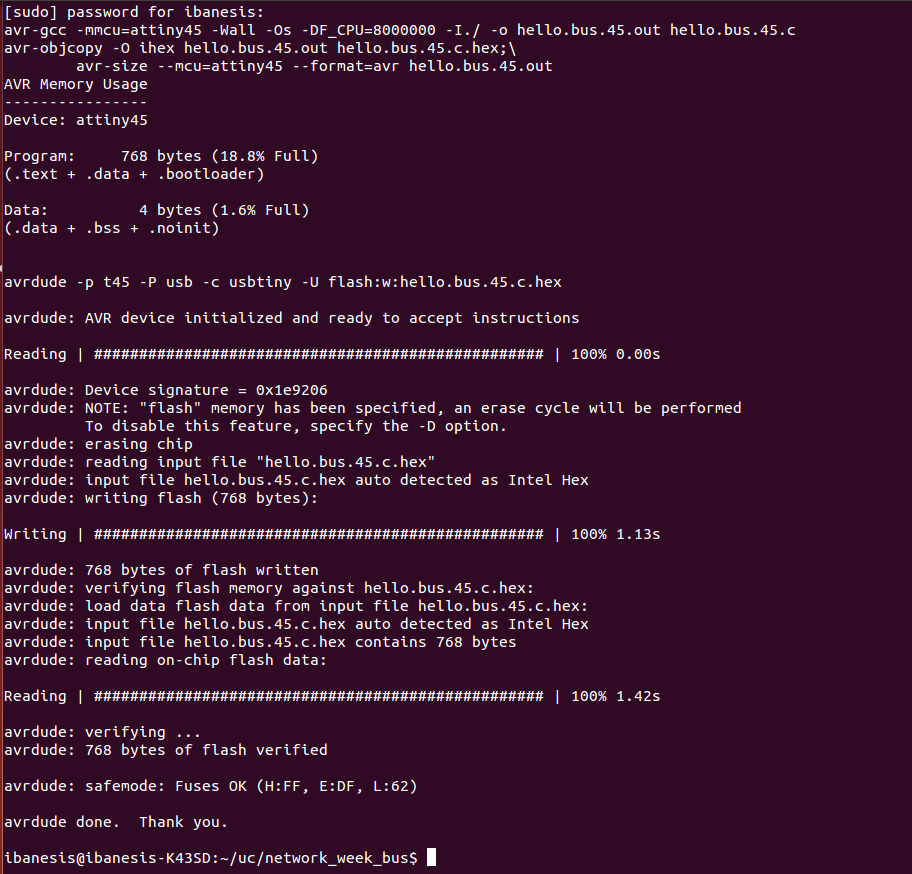
I used the example hello.bus.45.c and -make files from FabAcademynetworking and communications week.
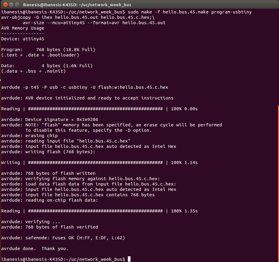
To program the board you need to type in therminal (opened in the same folder where you copied the c-file and make-file):
sudo make -f hello.bus.45.make program-usbtiny
You should get the response like this:
That was for the bridge. Now we need to flash the nodes. Each node operating has to have it's ID (you may set it in program. I typed "nano hello.bus.45.c"):

Let's see what will be the responce for trying to program the first node:
After we have flashed all the boards it's time to try them! We need to connect all the boards with wires and communicate with the bridge via serial port. I use arduino serial monitor on 9600 speed.
That's how it works:
The first problem I faced was spoiling one of the nodes while soldering. The problem is that I only had straight through-hole connectors and to solder them I had to bend them with pliers. It was hard to make absolutely same bands and it made the soldering difficult. That's why I kinda overheated one board and wrested out the contact pads. But I soldered connectors to the traces and I believe it is still possible to use this node, however it can not be connected with common wire.
Here are the board, traces and interrior from networking and communications

hello.I2C.45.bridge board |

hello.I2C.45.bridge traces |

hello.I2C.45.bridge interrior |
hello.I2C.45.node board |
hello.I2C.45.node traces |

hello.I2C.45.node interrior |
I fabricated this board with my laser-etching technology (Why not to mill? Here's the answer!), which is quite nice and fast. After I cutted the PCB outline in the laser cutter I etched the board till all the outline-copper was removed. And then I need to remove the paintspray with solvent and trim with file:
This time I decided to show you the etching process in stages:
The etching began... |
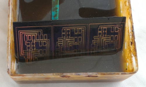
...some traces removed... |

...almost done! |
Then I cutted the boards with dremel:
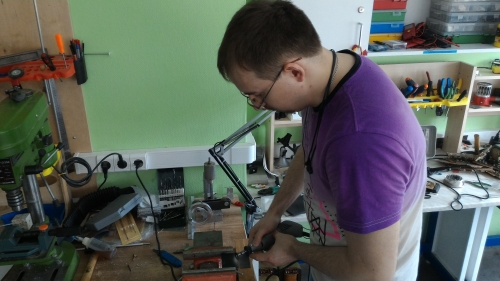
Thats' me cutting them with the dremel-tool |
Closer look |
Finally I have those boards:
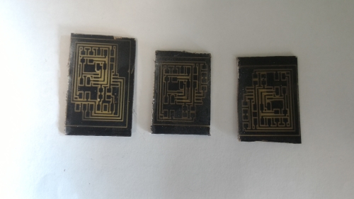
Roughly cutted with the dremel-tool |
Now they're trimmed and cleaned! |
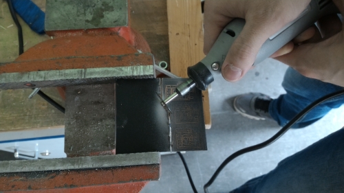
Then I slodered the PCBs:
The main difficulty was the electronic shipment: we were out of attiny45's and I had to purchase them. I did from one expensive shop in hope to get them on the next day, but it longed for four days. I understand that in some other places even four days for electronics shipments sound like a pleasant fairy-tale, but in Moscow I could try to find some other options to save some money in this time terms.
Back to my main page