Electronics Design Assignment
This assignment was in its own way, very interesting, as I was able to
get out of my comfort zone and learn a little more about electronics.
We first started from the Hello Board:
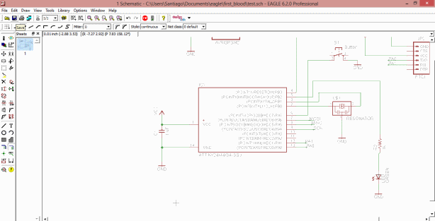
As I was
designing, I used the Board Reference model in this stage, which
helped. The ERC check showed warnings, not errors..
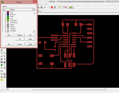
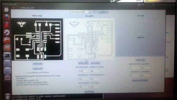
At that point, I did not know how to select which design layers would
actually be exported for the milling, so I ended with a PNG that would
need a lot of work erasing and cloning pixels to get it to proper
shape, fortunately, a friend helped me to correct this mistake. Still,
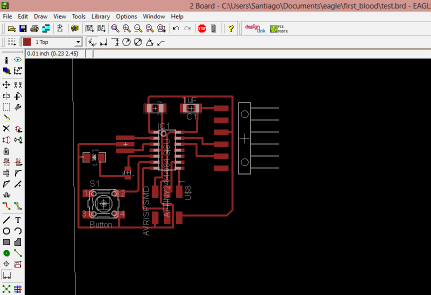
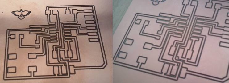
befor doing this, I realized I had made a few blunders in the milling.
Marked in red ther is a track was not properly designed. Correction was
in
order.
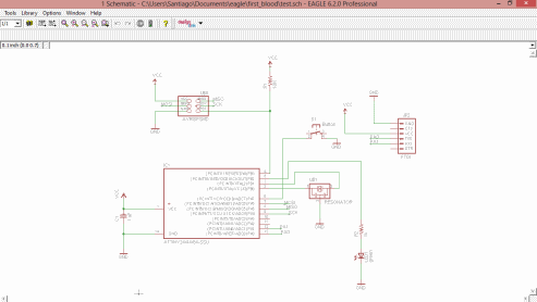
After correcting
the mistakes and selecting the proper layers, I had a PCB 90% ready for
milling:
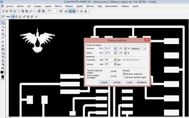
Just added a logo using a photo editing software and then I was ready
for milling.
I made two versions of the card, one as-is and other one with the same
dimensions as the hello board PCB in the academy website, in the end,
it was not necessary.
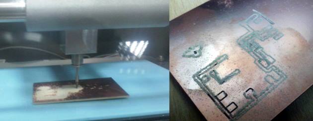
The milling was not to be without incidents, as the first plate I put
in the modela was not bonded strongly enough, and got loose as it was
milling, Modela 1 - Isaac 0.
After placing a second plate and checking it was properly bonded, it
worked, although the z-calibration was not optimal and the
tracks were not in its optimal shape, had to try again. The second
time, the tracks went better, but some residues were still in the
tracks, so some sanding was made before the plate could actually be
welded. But first I had to cut the plate using the 1/32' mill, for this
I created a new frame for cuttng:
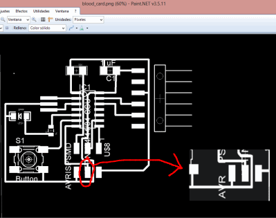
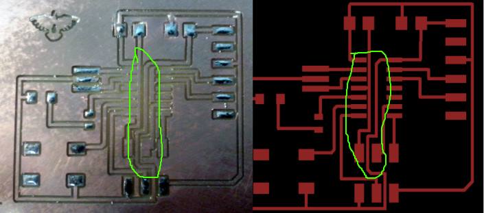
With this I had the plate ready for soldering... or so I thought. As I
was starting to add flux to the terminals I realized the center track
touched all of the Attiny terminals in the left side, when It was
supposed only to touch the fourth from the top, so the most
analog solution was to cut those threads using a scalpel, available at
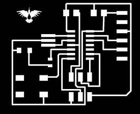
the lab. As a sort of Plan B, I modified the PCB design and changed the
routing, since what caused this was sending too many routes through the
center, under ther Attiny chip.
Modified Routing.
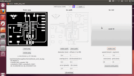
Afterwards, I sent the new design to the Modela, this time without
incidents.
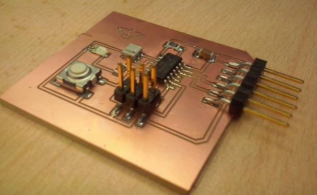
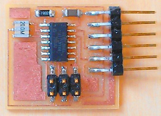
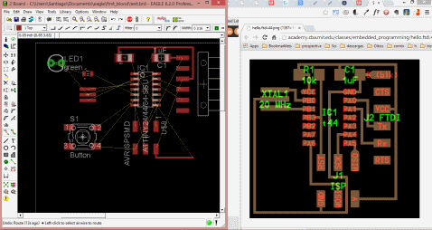
This time the tracks were well milled, no copper residues, no missing
tracks or separations:
Welding, as in
assignment number three, proved somewhat difficult, in particular the
resonator, since you need to solder all of the terminals underneath
it,and your visibility is not the best to do this, however, after some
fully-focused work, it was done:
As a sort of conclusion, I will say that, even though I learnt much
about electronics, there is still much to be learnt in order to get
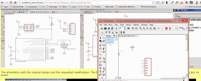
succesfully to the final project, also, The timeframe was not enough to
get to the circuit simulation, since the learning curve of the
necessary sotfware is somewhat steep.
|