

The discussion today focused on Circuit CAD software.
I'm going to do this in reverse order... I'm first going to show the PCB I made and the code I used to test it.
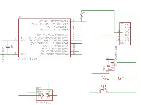
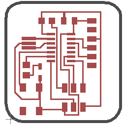
This is the board flashing the LED when I push the button. It worked just as expected.
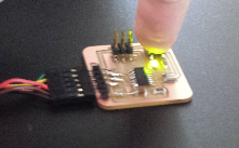
The code for this is pretty simple. When you push the button, the LED flashes. I have the code and some scripts used for testing available here. (I didn't use a Makefile, I just wrote a script for compiling, and then one for loading.) You'll of course have to change the PORT and direction registers to match your particular PCB design. I programmed this with my FabISP, so if you use a different programmer, you'll have to modify the "program.sh" file.
I have been using EagleCAD for the last 10-ish years, so I wanted to attempt using new software. First I want to talk about Kokopelli's PCB library. This is certainly an interesting way to make PCBs. Make sure you have the most updated version of Kokopelli and it's PCB library. Then you can open the example FabIPS.ko PCB. Play around with the values of the commands, comment out a line here or there etc. to see how things work. Then you can start your own design, stealing bits form the example as needed. The only part that wasn't available was the button. While I am partial to coding, I can't say that I think this is the best way to make PCB art. It adds a layer of complexity to the whole process as it is at the moment. Firstly, you need to draw out your design on paper or some CAD program, then code it in Kokopelli. Also, until schematic entry is added (possibly by incorporating PHDL possibly?) It is all too easy to miswire something in your PCB design. Other CAD tools allow you to draw the schematic, then from that, the PCB is created, which ensures that the correct pins are connected. If you do this all in your head, it is easy to get mixed up. ("Is the xtal between pins 3 and 4 or 4 and 5? Better look at the datasheet for the million+1th time to see..."). Overall, I think it is an interesting method of PCB creation though. One could argue it could be used for large complex PCBs, but I don't see it as particularly useful at its current state. One could then argue that it is best for small and simple PCBs, but then again, I'd say other tools are much better suited for this task at the moment. Further development could certainly change my mind though.
I downloaded KiCAD and though I had tried it several years ago, (as well as gEDA) I thought I would give it another shot. KiCAD's installation file is a couple times larger than EagleCAD, which I didn't like, but I expected this to be caused by better features. From this point on, I have a side-by-side comparison of KiCAD and EagleCAD and the process I used for each. (Click the images below for the full size picture.)
I drew the schematic and attempted to make the PCB. I didn't really find KiCAD's part selection process useful at all. I found it very tough to find a part because I did not like the interface of the parts selector. I could not see what the PCB footprint would look like for the part. I would later find that I have to manually select the footprints for each part, without being able to preview it.
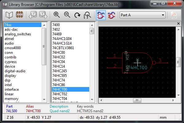
I found the preinstalled libraries from KiCAD rather anemic. Maybe this was because they are so hard to navigate that I couldn't find things I was looking for, or maybe the parts I was looking for didn't exist. I ended up finding a handy website that provided conversion of all of EagleCAD's libraries to KiCAD format. I Installed these and was able to find much of what I needed. they even have an EagleCAD user language program (ULP) that exports custom libraries so you can migrate to KiCAD if you choose.
KiCAD has clumsy mouse interfacing. If I bring my mouse too close to the edges of the schematic panel of the window, it assumes I want it to scroll in that direction. This is incredibly annoying.
I was able to pan left-right -up and down using the Shift and CTRL keys as I scrolled on the keyboard.
KiCAD does NOT keep your wires connected to the parts if you move them. In fact, each section of wire is independent and can be moved on its own. This is horrible user interfacing for circuit CAD! I'm not drawing houses that need like 10ft. walls or anything, the concept is more abstract; I am connecting a pin on part A to one on part B regardless of how far apart they might be. That should persist if I need to move the symbols.
I disliked that if I tried to delete something, I have to select from a menu what I want to delete, even when I obviously click the specific thing I wanted to delete.

KiCAD moving to PCB design from schematic to PCB *should* be easy, but instead it makes you select the PCB footprint for each part in your design. There is an "auto-associate" button but I hardly found it very useful. You have to select the specific footprint you want from a list of all possible footprints for all possible parts in KiCAD.
Click the "Preview Footprint" button to preview the footprints. The neat thing here is that this new window has another button to allow you to see the part in 3D.
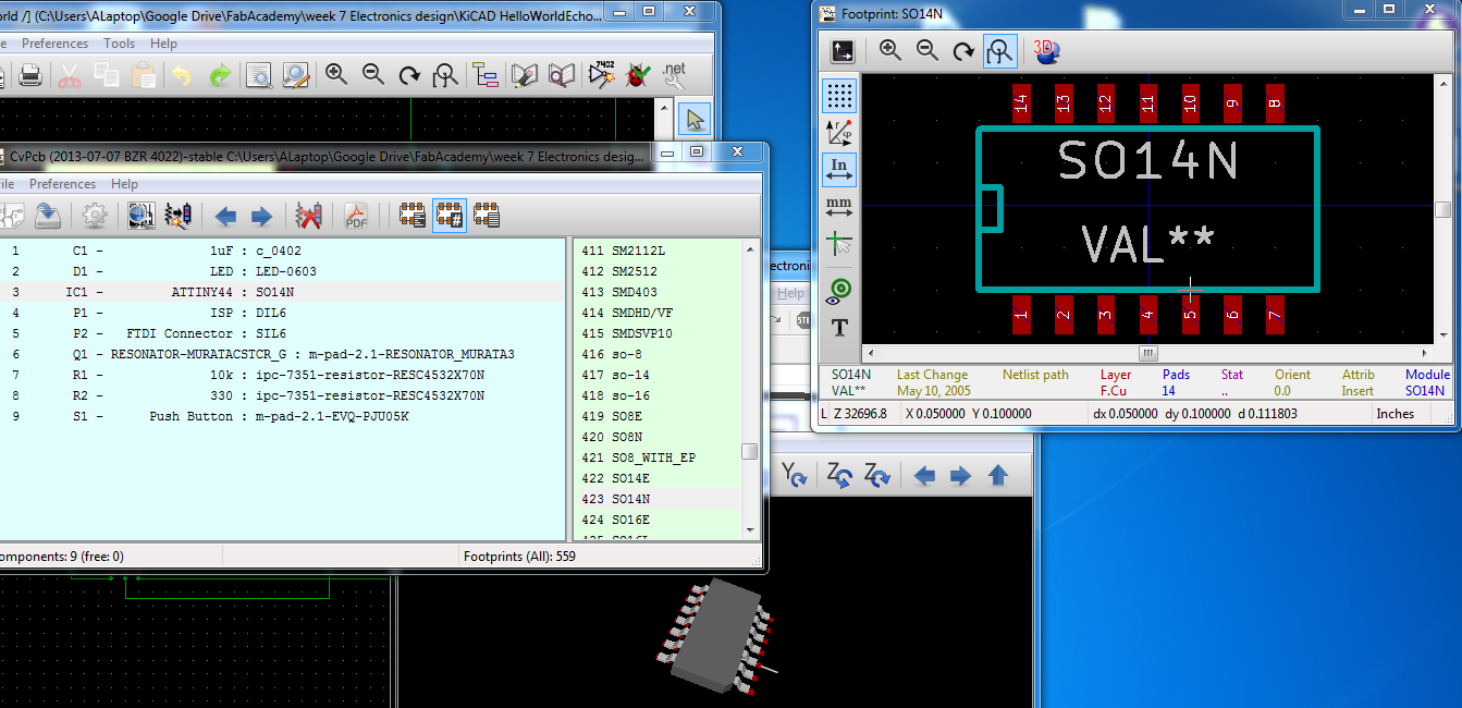
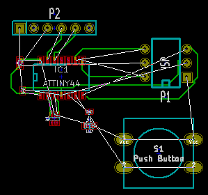
Overall, I did not find the PCB designer very usable. First you must import your net (there's a specific button to do so), then you have to use hotkeys when clicking objects to move them around. (hold 'm' when clicking an object to move it, click 'r' to rotate the part). Some of the footprints I chose would not import for some reason so I had to choose other similar ones. In the end, I stopped working with KiCAD because it wouldn't allow me to wire certain pads and I couldn't figure out why. Here are the results so far.
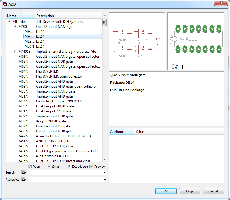
EagleCAD on the other hand has a (only slightly) better parts selector with a search that actually seems to work (as long as you already know what the part is named in a library) and shows both the schematic symbol as well as the PCB footprint of a part.
Many places online provide EagleCAD libraries for parts they use
or sell. FabAcademy,
Sparkfun,
Adafruit,
and many other places
freely distribute their parts libraries online which can save a user a
lot of time and energy! Since I've been using EagleCAD for years, I
have my own personal library of parts, which is really small compared
to the others I linked to, but I use it all the time.
I actually had to modify the Fab.lbr file from fab academy because
the pins of the SOIC14 chip were too close together. If I think about
it when I am on my other PC I will post it on this site.
EagleCAD lacks the ability to CTRL + scroll or SHIFT+ scroll to pan left-right and up-down. This has always bothered me.
At least when I move my symbols they stay connected.
A new thing I learned was that you don't have to draw lines to every part. Simply draw a short wire on the end of any pin and rename it with the naming tool. Using the naming convention (like in Xilinx) any other wires with the same name are connected together internally. This cleans up your schematic designs but still keeps those parts connected on the PCB.
This is as simple as clicking a button in EagleCAD. Since you choose which footprint you would be using when you selected your part, click a single button and EagleCAD will plop the footprints down on the PCB workspace. Arrange these any way you want and if you want to be lazy, just click the "Autoroute" button, select "NA" for the bottom layer and click"OK" at this point EagleCAD will draw your schematic for you. If you won't like it you can edit it with the "Ripup" and "Route" tools. Or you could just Undo the autoroute, move your parts and try again.
When you finish with your design, EagleCAD has multiple export
features. Most board houses prefer Gerber files, and several websites
provide nice custom CAM processors to export things correctly such as
Sparkfun
and OSH Park (AKA Dorkbot PDX).
In our case, we will be useing Fab Modules, so we should export
PNG files. Be sure to add the outline of your PCB before exporting.
First, select the "wire" tool and in the top left corner change
the layer from "Bottom" to "Dimension" and select the "thickness" as
0.032inches. You need both of these in your PNG at first
to keep the same image size and reference point of (0,0) for the PCB.
Click the "layers" icon (blue red and green icon up at the top
left corner) Select "none" then manually click
on "Top" and "Dimensions" layers so they are the only ones
highlighted. Click OK and this should leave you with
something similar to my PCBabove. Once these layers are selected,
click File-->Export-->Image. Click "Browse" and select the
folder you want to store the image in and name the file. Then make
sure the "Monochrome" box
is checked and enter a relatively high value for
DPI like 500-600 or so to get a good quality image. When
done, click OK.
Go to the image you just made and open it in a paint program such
as GIMP. Make everything white inside the dimension line (leaving the
dimension as the only dark line in the graphic) and Save
As... "cutout.png"
Now undo those changed and white out the cutout line so that all that is left is the circuit
itself. Then invert the colors (in GIMP, Colors-->Invert
or Value Invert) and save as
"traces.png". Now you are ready to mill these in the Fab
Modules.