Electronics Design
Assignment
Redraw the echo hello-world board, add (at least) a button and
LED (with current-limiting resistor), check the design rules, and
make it.
Ideas and Approach
I decided to make a board that would be quite versatile. I
wanted to make it so that I could exchange inputs and outputs to
test certain components. To that end, I wanted to have 2 2x2
headers (one for inputs and one for outputs). And with each
of these headers, I wanted to have one analog and one digital
"port". That way I could easily attach new components and
test. I am ultimately hoping that this is something I can
use to teach students how all this works using simple connections
(e.g. just connecting a component to a header).
Design Files
Steps Taken
On the Thursday night after the class, I headed down to AS220
where Shawn (our awesome TA), gave us a great rundown of
electronics/electrical components.
|
|
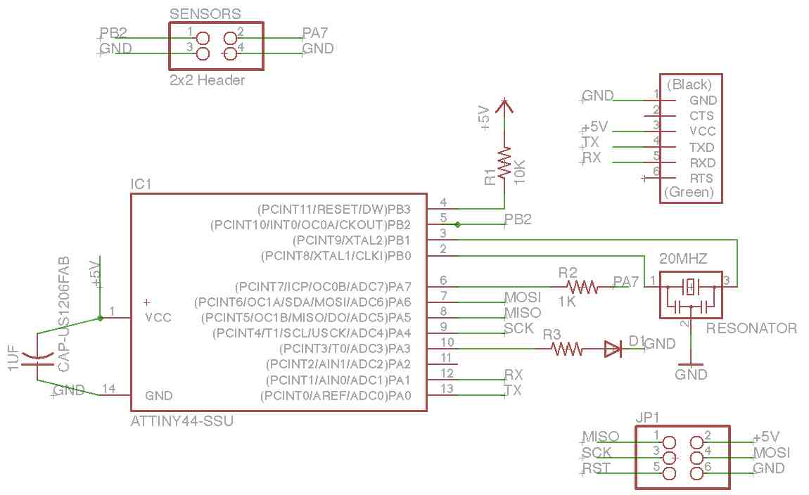
Here's my first draft after leaving
AS220. After not thinking about it for a day and a
half, I went back and reviewed what I had. I realized
I had a few things that were wrong or could be better...
1) There were some traces I realized would be near
impossible to solder. For example, the following
connections/traces wouldn't really work because they had
interior connections that I wouldn't be able to solder...
- pin 9 of the ATtiny
- pin 4 of the 2x3 jumper.
- pin 3 of the
...wait...now I feel like an idiot. I am wrong.
The big areas are the pads that will be soldering to so it
doesn't matter what side of the pad the trace comes in
on. Doh...
2) I realized I should label some parts so that I'd know
what they are when attaching things later on. For
example, I should mark which jumpers are for each pin.
3) I realized there might be some places that I could add
more space to make the soldering a bit easier (e.g. the
crystal & ATtiny are REALLY close). I realize the
crystal needs to be close, but I can move it a small amount
to the left.
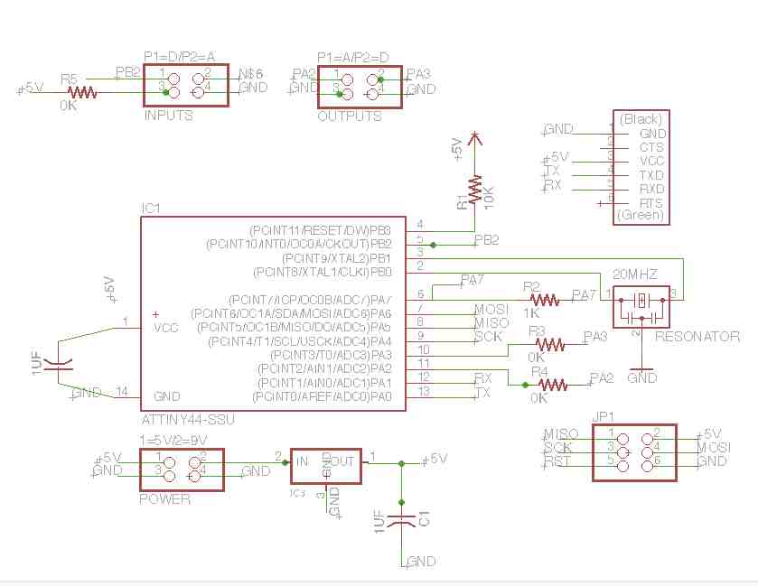
4) I decided I want to add a second 2x2 header for outputs
(one analog and one digital).
|
|
|
1) I did the pull up resistor wrong. In
general each Analog input needs a +5 (for pullup), GND and
Signal value when doing the header.
2) My R3 resistor wasn't doing anything of value so I
changed it from 1K to 0K ohms (thanks to Shawn for
explaining this).
3) I found I was wrong about labeling. It turns out
you don't want the labels. It messes up the traces if
the words go across the board. Obvious when you go to
mill the board and you see the pictures.
4) My regulator/capacitor connection was wrong. I
through it was supposed to sit in serial in between the
regulator and +5V. That's wrong. It is actually
supposed to be in parallel.
|
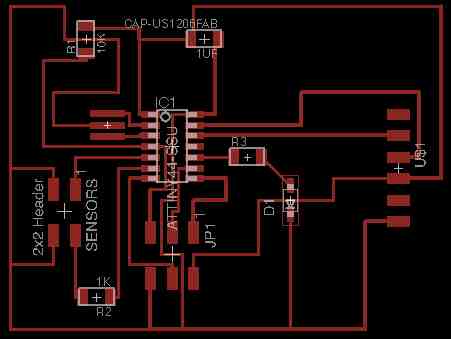
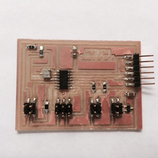
Once I had the board design, I milled out the board and stuffed
it. Here was the final result. I felt much better
about this one because I ended up getting it right the first
time. No jumpers. No big mistakes. And when I
plugged it into the programmer...yeah!...I was able to burn the
bootloader.