Fab Lab Barcelona SuperNode /Fab Lab Sevilla /Jose Perez de Lama
[assignment]
Redraw the echo hello-world board, add (at least) a button and LED (with current-limiting resistor), check the design rules, and make it.
Hello world board, echo.hello.ftdi.44, links:
hello.ftdi.44.cad board components traces interior
Link to class syllabus:
http://academy.cba.mit.edu/classes/electronics_design/index.html
[preliminary comments]
The sixth class wasn't encouraging for me. I have very little experience with electronics and the class didn't really add a lot of practical knowledge, but then we had to begin an assignment i didn't have a clue how to approach... Some experience with Arduino, some readings... But no real practical previous practical experience or theoretical studies.
The evening after the class i downloaded the Make: Eletronics book, by Charles Platt, and started reading. It had been recommended by the authors of the Arduino Projects book, which i have to say as well is an excellent written and designed book, and package for a first approach to Arduino. I stayed reading until late, and felt much better, even excited; and of course a bit challenged like every week in the Fab Academy.
[assignment development]
I had downloaded Eagle some weeks ago, and i even had a funky photocopied tutorial that i had bought as a souvenir during Fab7, in Paruro, the popular electronics market in Lima. But then, as i would have had to begin from scratch and i was quite curious about how it was to script the boards Neil's way, i opened with Fab Modules the .cad file of echo.hello.ftdi.44 and started reading the code. If you copy this piece of code in a Open Office processor, it is 81 pages long. But as one reads along slowly, one can realize it structure, and then at the end, there is the actual code of the board, a couple dozen lines of code, which somehow look like placing components, and then wires, with x, and y coordinates on a board...
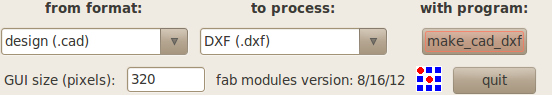
[designing the board with Fab Modules]
So i started to study how this had been donde by Neil. At the beginning of the 81 pages, after the credits and terms of use you find some lines to choose which is the output you want to get: components, traces, interior...
Then you have the "presentation" of all the geometries and operators [such as add, substract, rotate...] with the variables or parameters that you need to input to define any of these.
Then, you have the actual code for each of these objects or operations; not so sure about the name. A mathematician friend, to whom i showed it later, observed that concerning the geometries it defines a region, and not so much a surface. Yes, i told him, this method is called f-rep...
Then, you find the electronic components library, beginning with the pcb board, where the components are geometrically defined, including some specific characteristics of them, such as the model names for the connectors, and the ICs.
And eventually, you find the actual definition of the board, the components, and the wires.
To finish, there are some geometrical data for the representatuon, like xmin, ymin... THis is a very schematic description, of course.
But then one, that allowed me, first, to test some modifications on NG's file, checking the png outputs, and in this way, understanding how the coordinates of the components were described; and then finding the actual new components i wanted to include, being able to write them in as well as the "wires" connecting them.
Actually the afternoon before, besides reading Make, i had been checking last years and the year before last exercises by former Fab Academy participants, looking for some that i could understand and that were reasonably well documented.
My friend David's from Asturias, looked very cool, but i didn't understand how it worked. The examples from 2011 seemed to be made with another processor. Heloisa's and Nerea's from Barcelona, looked very cool... And eventually i found Natalie Haddad's board which looked very straightforward. She also mentioned it was done after Providence tutorial. I studied it a bit, and decided i could probably make it. E-mailed her, we had met in Lima, and she confirmed it had worked pretty well...
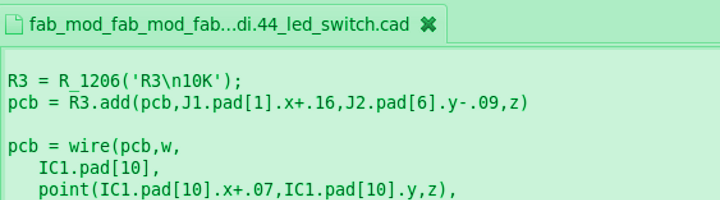
So, i spent the whole of Thursday studying Neil's code. I redrew each component in Rhino, to understand how it is described. If you draw it you realize it is "simple". Each component is defined as a class. It has a geometric center and a characteristic "pad" that repeats itself within the component with succesive numbers. For example an R_1206 resistor is defined like this:
pad_1206 = cube(-.032,.032,-.034,.034,0,0)
class R_1206(part):
#
# 1206 resistor
#
def __init__(self,value=''):
self.value = value
self.labels = []
self.pad = [point(0,0,0)]
self.shape = translate(pad_1206,-.06,0,0)
self.pad.append(point(-.06,0,0))
self.shape = add(self.shape,translate(pad_1206,.06,0,0))
self.pad.append(point(.06,0,0))
One can see, the 0,0,0 for the center, and then how the pads are placed relatively to it. When it comes to more complex components, as the ATtiny44 microcontroller, it works the same. But there is a lot of good information in the class definition like the pad numbers of each pin, and its names.
The wires are a particular case. They are defined by the width "w" and the points it goes through. Neil has built in some algorithm that autoroutes to a certain extent the paths and connections to the pads.
The points you give in x,y,z coordinates, for both components and wires [z being in this case always the same and defined at the beginning of the pcb description]. The x, y are usually given relative to the previous components coordinates. They can be defined referenced to the center of the components or to each of the pads attaching the corresponding number.
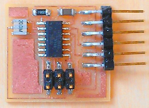
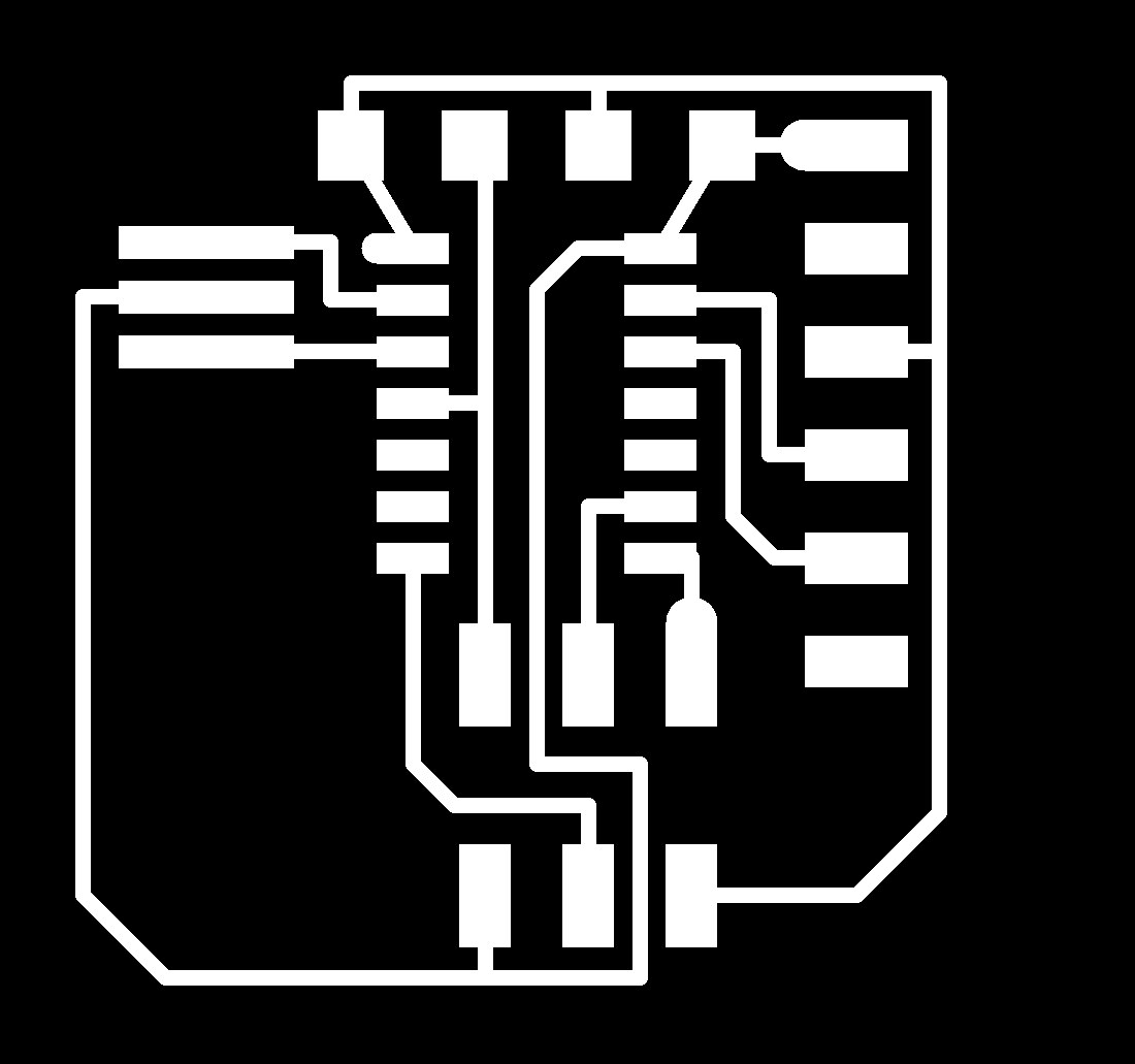
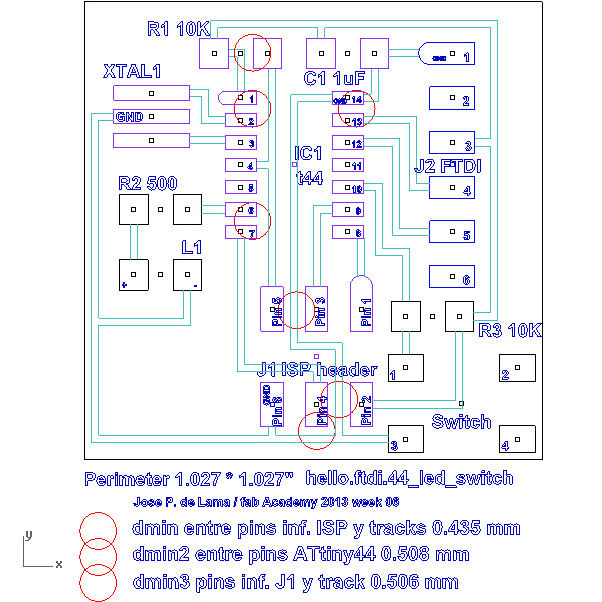
So, finally i generated my own board scripting it with Fab Modules / Kokopelly language. Following Natalie's example, i added a second resistor and an LED, connected to PIN 6 of IC1 tty, and a third resistor and switch button connected to PIN 10 of IC1.
The list of components for the board is as follows:
| Resistors |
||
| Num
units |
Component |
Digikey
ref |
| 1 |
R1
10K
/
RES
10.0K OHM 14W 1% 1206 SMD |
311-10.0KFRCT-ND |
| Capacitors |
||
| 1 |
C1
1uF
/
CAP
CER 1UF 50V X7R 10% 1206- |
445-1423-1-ND |
| Crystal |
||
| 1 |
Crystal
20
MHz
/
CER RESONATOR 20.00MHZ SMD |
XC1109CT-ND |
| Microcontroller |
||
| 1 |
IC1
t44
/
ATTINY44A;
IC MCU AVR 4K FLASH 20MHZ 14SOIC |
ATTINY44A-SSU-ND |
| Connectors |
||
| 1 |
J1
ISP
/
2x3
connectors / SMT or CONN
HEADER 4POS .100" DL SMD
|
609-4463-6-ND |
| 1 |
J2
FTDI
/
6
connectors / CONN HEADER 36POS .100 R/A SMD |
S1143E-36-ND |
| New
components |
||
| Resistors |
||
| 1 |
R2
499K / RES 499K OHM 1/4W 1% 1206 SMD |
311-499KFRCT-ND |
| 1 |
R3 10K / RES 10.0K OHM 14W 1% 1206 SMD | 311-10.0KFRCT-ND |
| LED |
||
| 1 |
LED
/ LED RED CLEAR 1206 SMD |
160-1167-1-ND |
| Switch |
||
| 1 |
Switch
/ SWITCH TACTILE SPST-NO 0.05A 24V |
SW262CT-ND |
[workflow]
Finding the right idea / model for the design > scripting the new components on Fab Modules .cad [module cad to dxf] > Fab Modules generating png > Fab Modules generating path with milling parameters > generating dxf > opening dxf in Rhino, making minor modifications to fit iModela > exporting to .ai > opening the .ai file in iModela Creator and setting milling parameters > placing board in the iModela > calibarting the z > opening iModela Controller en setting x0, y0 and z0 > milling! > selecting the components > stuffing the board.
[milling]
Milling process has been long because we were still taming the iModela, the available mills, and what precise parameters to give to the path file in Fab Modules and the iModela software. Finally, i ended up "doctoring by hand" the Fab Modules generated files, to allow for wider separations in critical points - identified after several milling tests.
General parameters were:
Milling diamater = 0.4 mm
Offsets = 4
Overlap = 0.5
Cutting depth = 0.01 mm and 0.02 mm [for different tests; after very cerafully calibrating the horizontal plane in the iModela, we achieved good results with both, even if our mill is 45ª angle, with an end o 0.2mm.
Here is a visual synthesis of the process:
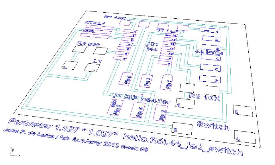
Rhino study based on Neil's .cad file. Translating the components dimensions and placement descriptions
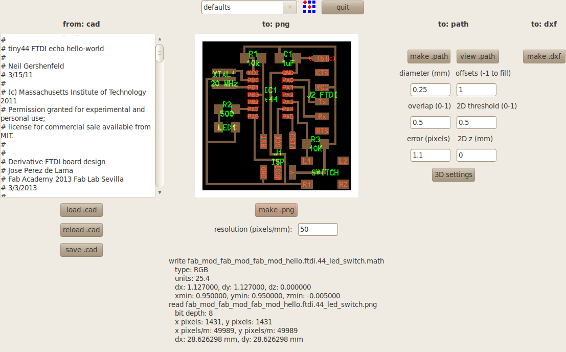
Fab Modules .cad to .dxf. Modifying the original file and checking png outputs.
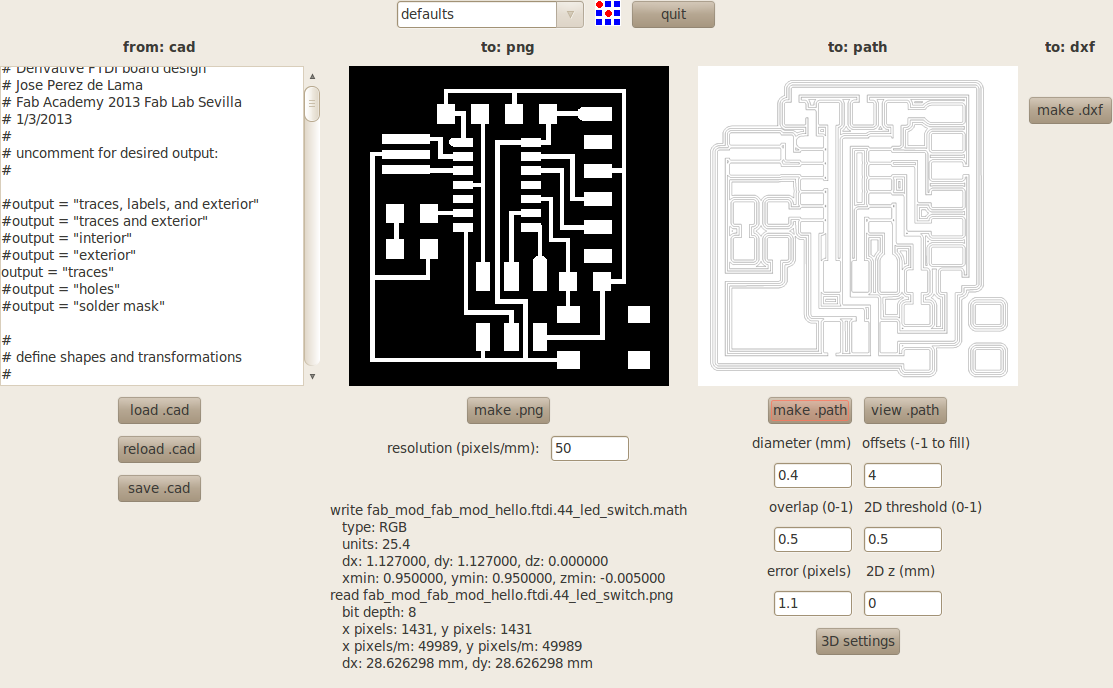
Generating "traces.png" and paths with default parameters
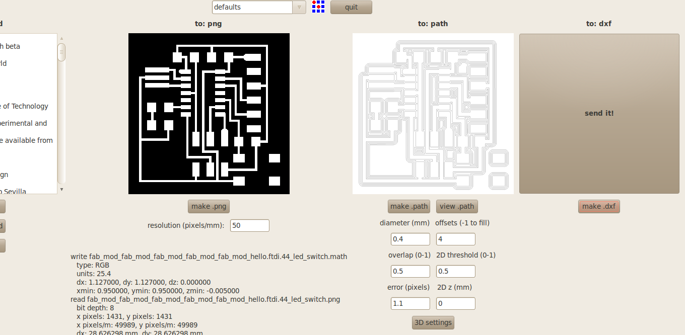
Make dxf!
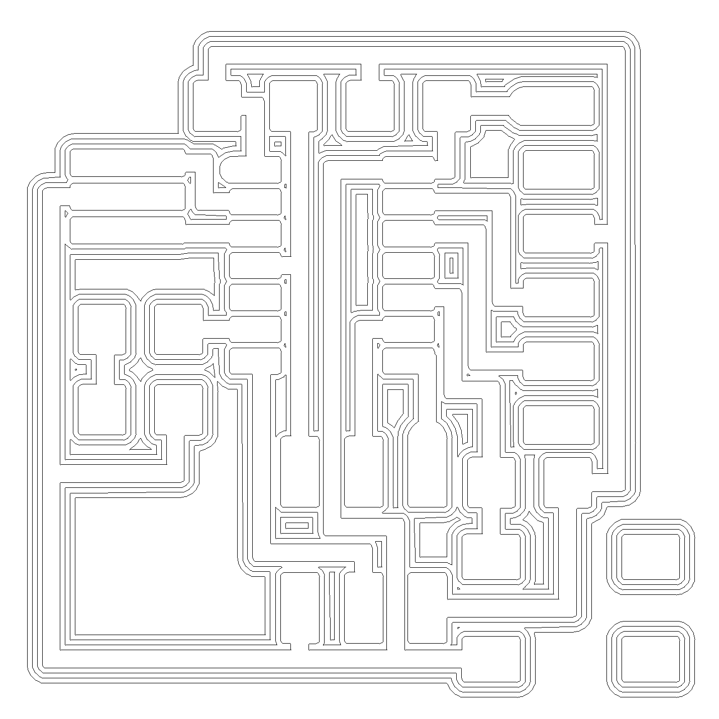
Fab Modules generated milling path file. Diameter = 4mm; Offsets = 4
Rhino study of critical point for milling
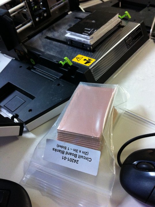
Geeting ready for milling with the iModela and FR1 boards from Inventables
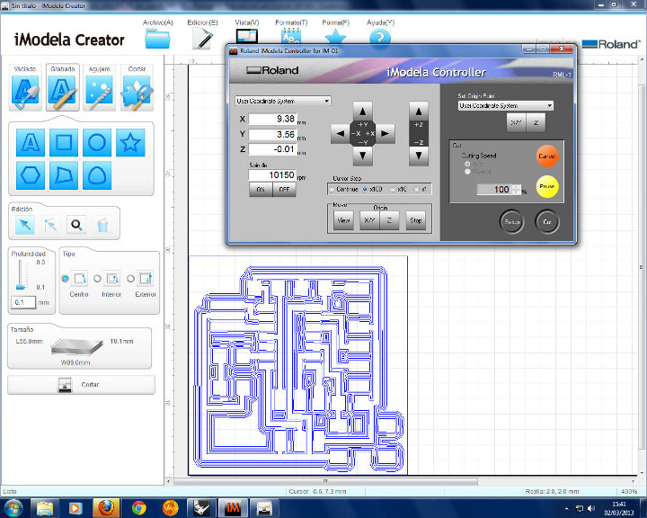
iModela Creator and Controller interfaces, with "doctored" path file.
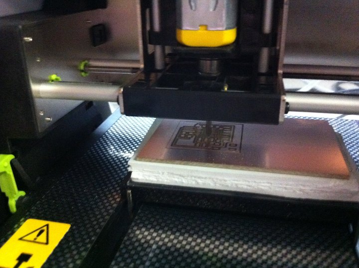
Milling one of the final tests with the iModela
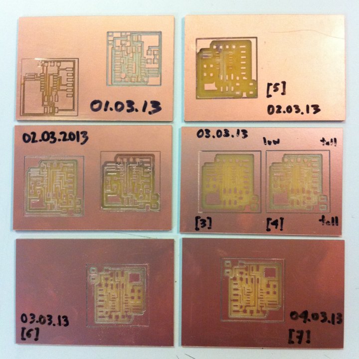
Several tests. 6 and 7 are almost there... Final improvements in the process were using a new mill, choosing a [acrylic 5mm] sufferer with very good horizontality, with a z maximum difference lower than 0.04 mm, and modfying "by hand", with Rhino, the paths in some of the most critical points, making them wider than they actually "should be", to compensate for the 45º angle mill.
Picture is not very good, but this was one of our best boards, probably test 8 or 9. We achieved good results eventually with 0.01 and 0.02 mm cut depth; 0.02 milled in to steps. Next time i am sure we will be much more efficient! But i guess we will make new mistakes too!
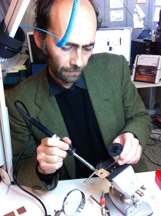
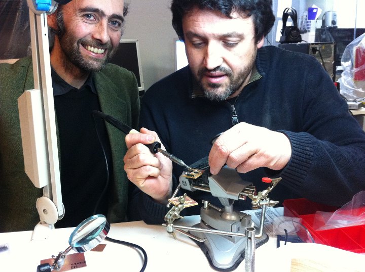
Team work soldering with Juan Carlos Pérez. Actually one of us was holding the components with clippers while the other soldered. This is a picture taking by Juan Carlos' 6 years old son Darío.
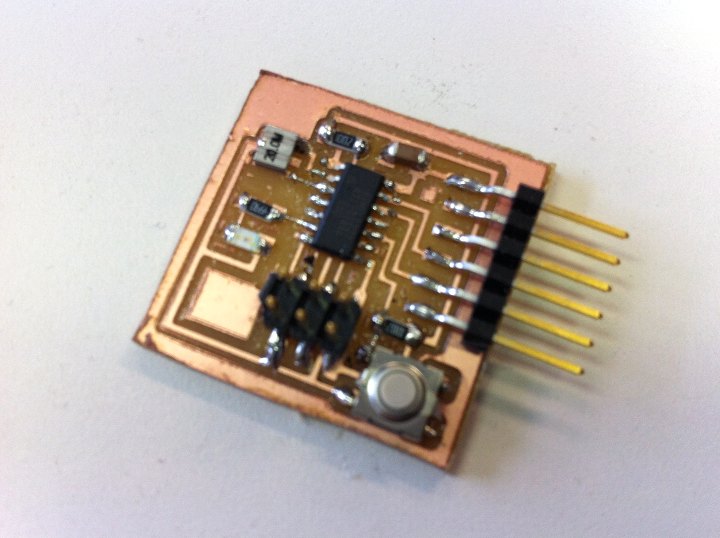
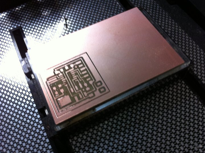
And this is the board Juan Carlos and myself managed to solder!
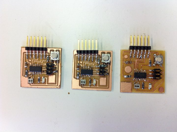
Team production for week 06. We will improve pictures for next weeks... These are cell phone pixs...
We haven't tested the boards yet. But it has been my first board with smd components, and i felt very proud when i finished soldering it!
[additional work]
For the final project i designed and fabricated a PCB that integrates two switches and 5 LEDs, completing the work done on week 06. The board can be seen here: link
As mentioned before i also made significant improvements milling the boards once we got a special adapter from Roland that allowed us to work with 1/64" end mills instead of the 45º mills we were using during most of the Academy. The results can be seen in the former link, too.
[files download]
Information and files are downnloadable under a Creative Commons Attribution-Share A Like license; attribution: Jose Perez de Lama / Fab Lab Sevilla / Fab Academy 2013
The .cad file is a small addition to Neil Gershenfeld's echo.hello.ftdi.44.cad file. It is a beta version.

# echo.hello.ftdi_led_switch .cad file [.cad]
# echo.hello.ftdi_led_switch.path.png [.png]
# echo.hello.ftdi_led_switch.dxf [.dxf]
More files available if anyone needs them.
Software :: Fab Modules .cad > .dxf; Rhinoceros; iModela Creator & iModela Controller
Hardware: iModela, with 0.2mm 45º mill
return home /perezdelama.jose