Week 08: Electronic PCB Production
Assignment
Group Assignment
- Characterize the design rules for your in-house PCB production process: document feeds, speeds, plunge rate, depth of cut (traces and outline) and tooling.
- Document the workflow for sending a PCB to a boardhouse
- Document your work to the group work page and reflect on your individual page what you learned
Individual Assignment
- Make and test a microcontroller development board that you designed
Learning Outcomes
- Described the process of tool-path generation, milling, stuffing, de-bugging and programming
- Demonstrate correct workflows and identify areas for improvement if required
Reflections
I have produced two different PCBs. One was in Week08 for Electronics Production week and the second one is in week11 and week12 where we have to make a machine. The first experience was incredibly smooth and enjoyable. It definitely motivated me to start learning about Kicad as well as how to put a circuit in a PCB together.
However, the second experience in the 11th week has been horrendous. Everything that could have gone wrong in my mind went wrong. After initially feeling excited with my own PCB schematic Dani had to make some changes as I didn't have enough pins in my SAMD11c to have both networking and switches, and PIR and test LED, so he showed me a way to share pins. This was interesting and I felt it increased my understanding of how a schematic can be designed.
Then moving to the PCB design. I had to draw all the traces. Initially I was worried about making sure the traces arrived at their destinations. Later on I realised I was wading into a circus of issues.
Firstly, the traces needed to be wider, lets say 0.4mm instead of 2mm. I learnt how to highlight a trace, then with Command U highlight any others traces connected to it. Then If I used command E a box would pop up and one could alter the widths automatically to a desired length...0.4mm.
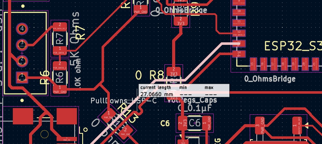
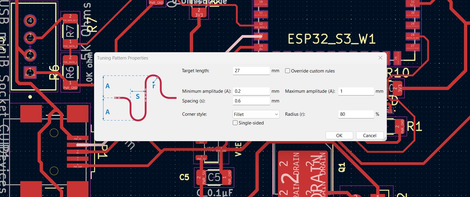
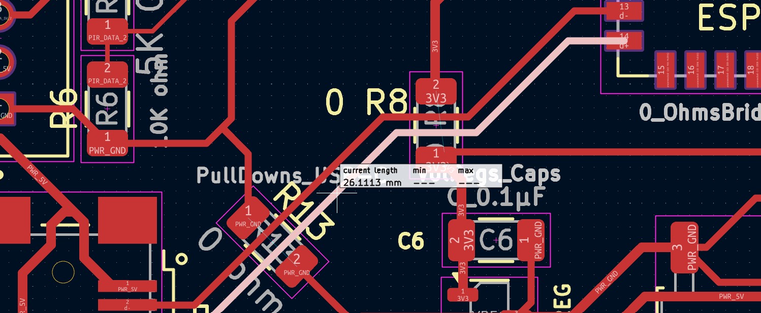
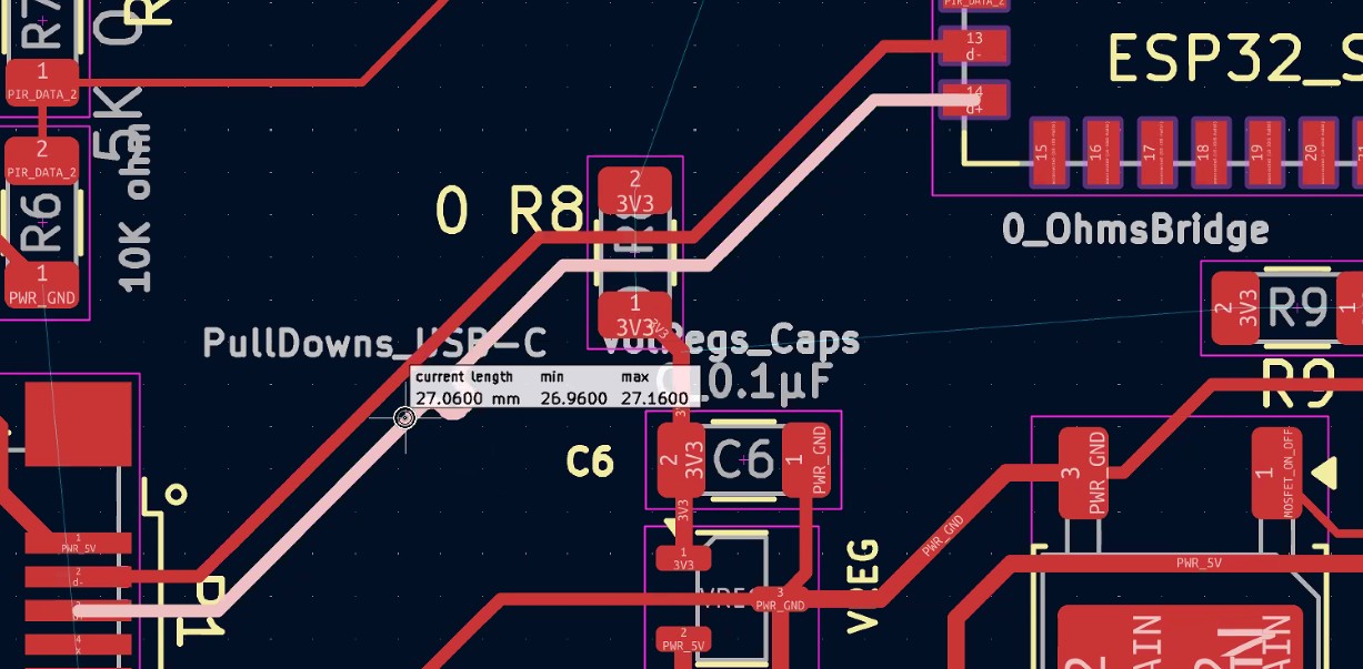
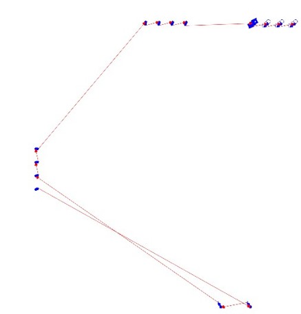
There was one issue that emerged. The D+ and D- traces were different lengths. One was 22.9mm and the other was around 18.3mm. As i understood it from Dani this was unacceptable and could cause issues or lack of function in the circuit. There was a nice tool one could use called Tune. One goes to the Route drop down menu, and then click on Tune a single track.
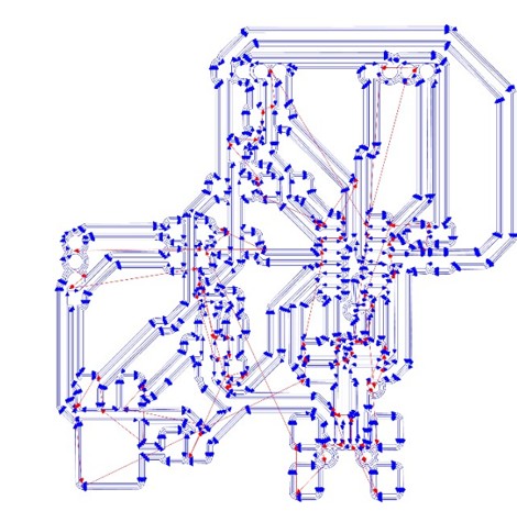
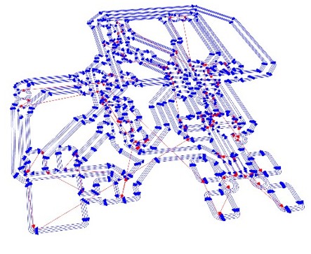
The following images are an example from another chip I am designing of length tuning.
It is where the D+ and D- lengths are different. We need to tune them to the same length (within an accepted tolerance) otherwise it can lead to signal degradation and potential data transfer issues. Specifically, if one line is significantly longer than the other, it can create impedance mismatches and delay differences, affecting the signal's integrity. This can result in reduced data transfer speeds, data loss, or even communication failures.
So we measure both lines, and then seek to lengthen the shorter one by inputting a target length (based on the length of the longer line). The software automatically gives us a length range that we must match.
After this was all done on that created issues because i had not realised that each element in the PCB design has its own kind of courtyard which reflects where the end mill will do its work. The Traces were now encroaching on those aforementioned courtyards which can only be seen when the element is highlighted on purpose. One has to be aware of this as something to look out for - and thank the Fab Gods that Dani Mateos was there to diagnose the issue and help me sort it out. I am the wiser for it.
Finally I exported the PDF format at 1000dpi of the PCB design and then brought it into Inkscape. The goal was then to create layers. It was sheer pain in the you know what - I'd like this part to be automated. It's one of my least favourite things. Spoiler: I almost felt ok about it by the end, and I think it won't be too bad in the future. So i separated everything into layers Outline, Background, Holes, Traces, and I had some layers for anything I didn't recognise.
I thought it was good and went straight to printing - some of the holes had printed without the coppers. Guess who came to the rescue? Yes, you guessed it. Dani was able to help fix the issue by increasing hole sizes on the PCB design in Kicad again. And somehow there were many additional layers in the Kicad PCB design which had to be deleted and were obscuring the hole sizes. In fact we realised that the holes were not perfect holes and that can cause an issue when generating the G-code as the modsproject.org software might not even recognise a hole...Yes, this happened to me too and the warning was that it generated a 1kb file - So like Groundhog day, I went back again to the PCB design, got through Inkscape and making layers fairly unscathed and then exported HOLES OUTLINES and TRACES PNG files into the modsproject.org software. Finally everything was set - I just needed to mill the PCBs.
As it turned out it was not perfect and a few more prints didnt work. I had to keep throwing away my boards.
The issue was solved by changing the machine.
I like to be on top of my business and so I am quite disappointed in suddenly getting behind with this task. It has affected my INPUTS, OUTPUTS and NETWORKING WEEKS - in those weeks i was able to make something happen, but it was not with my own board and hence not finished.
I now have my own functional board and ready to soldered the components on. Surely nothing can go wrong! Stay tuned for Part 235....!
I need to solder, flash the chip and then do some input, output, networking related thing.
Hero Shot
Process Documentation
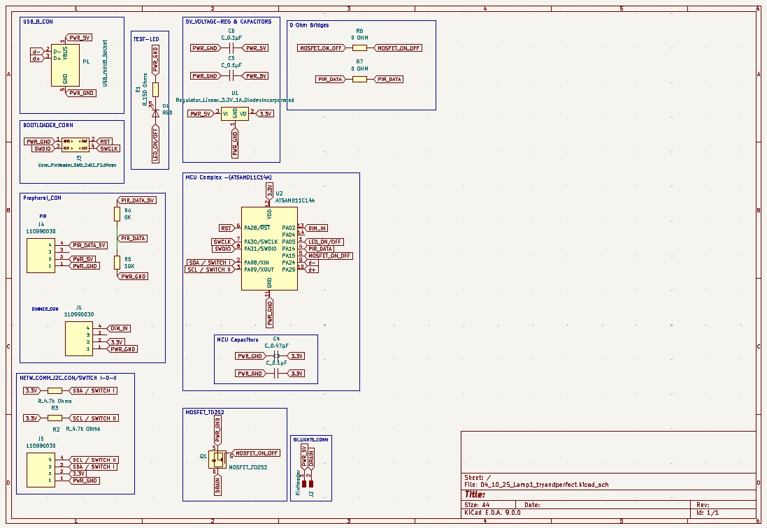
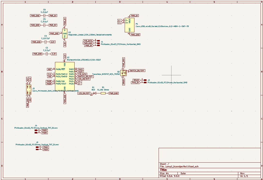
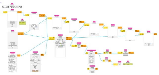
This is the schematic I created for the lamp with PIR sensor which is the basis for my PCB schematic
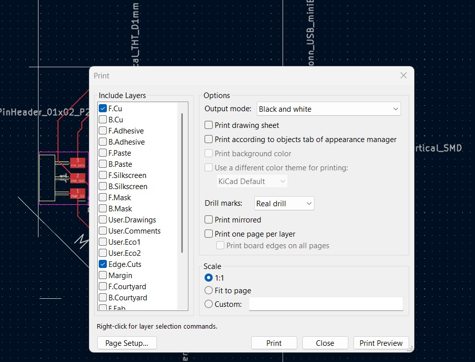
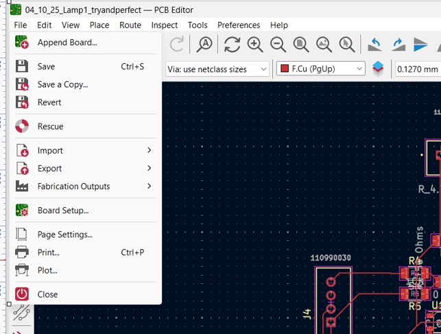
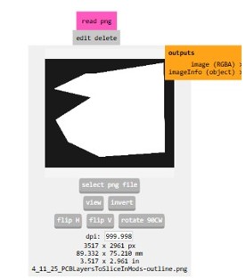
Once we have the kicad file of our board we must export it as a pdf. I exported the file from kicad.
I went to file, then Print and a box pops up. I made sure to include my Copper Layer as well as the edge Cuts and then clicked on Print.
The exporter processes the file into a pdf format
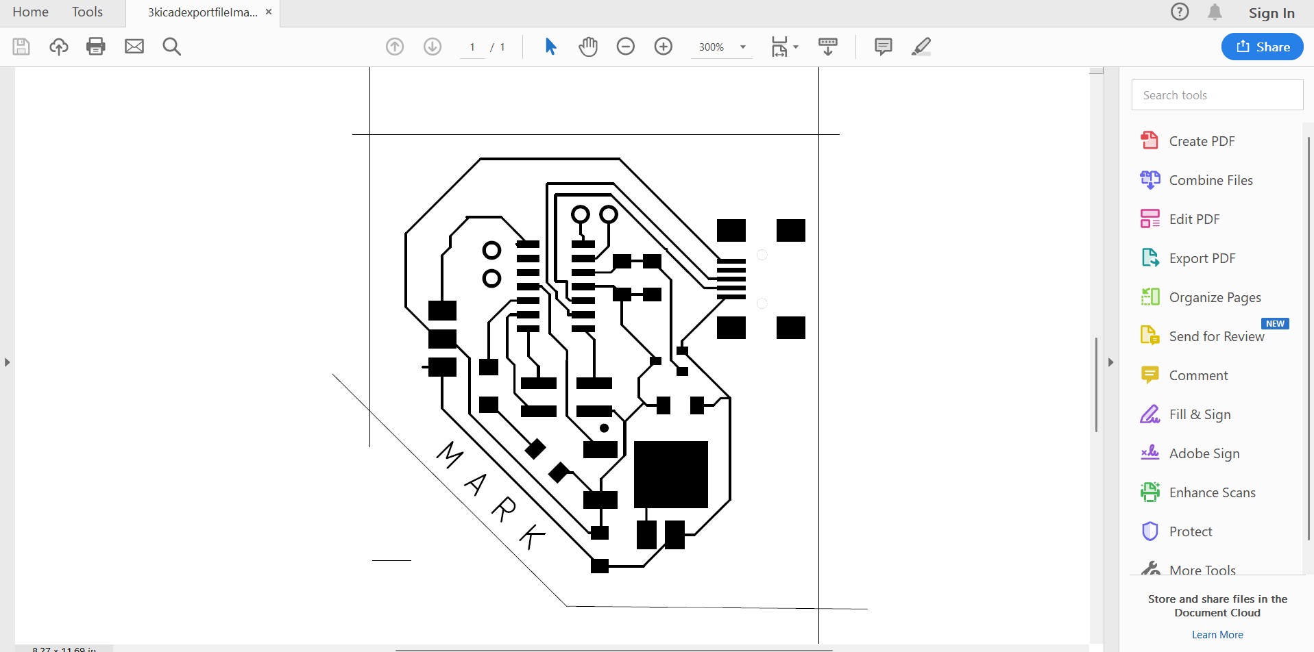
In Pdf format all the different parts of the PCB such as the traces, holes, and outline are all bunched together. So from here we must separate the files into their respective layers and create PNG files – from there we take those PNG files and slice them in modsproject.org which is an online PCB slicing software.
When the Pcb is cut, different layers will need to be cut with a different end mill and therefore in a different order. We use software such as Illustrator or Inkscape to create the layers in different files.
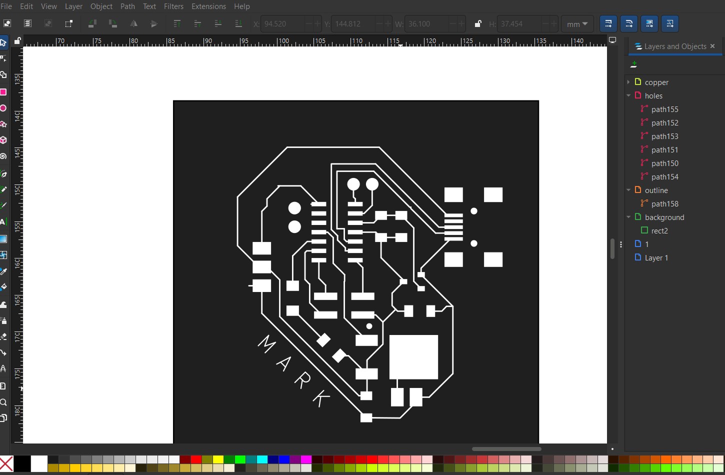
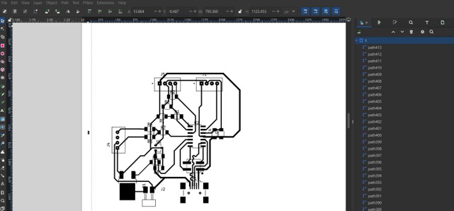
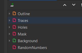
As you can see from the screenshot I created several layers on the right. I have an outline layer, a hole layer, a Copper/Traces Layer and a background, a copper (traces) layer, an outline layer, a background and Layer 1. Initially we select all and all the paths go into Layer 1. Step by step we highlight the holes and put them into the holes layer and then the outline, traces and create a background too. So by the end, Layer 1 will be empty and the other layers will have their relevant paths in them.
If we start with holes for example, we find a hole and right click to 'select similar' which highlights all the other holes – we then move to layer.
Once all the layers are ready, we want to export each layer to a PNG file to slice.
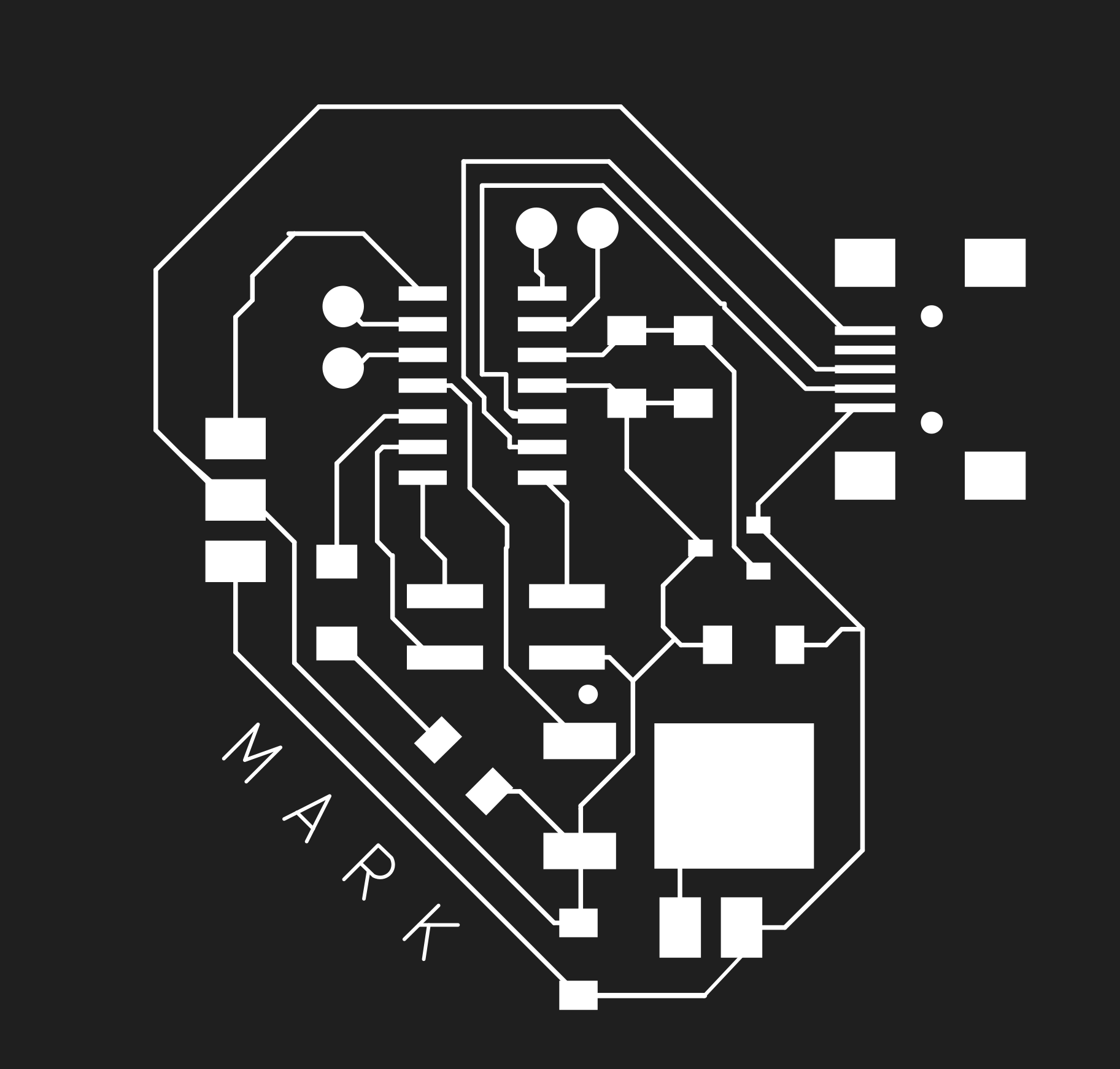
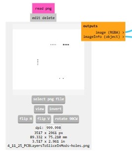
First we select the holes layer and make sure the background is white and the holes are in black and we export as a PNG.

Then we create a black background and a white body for the Outline PNG.

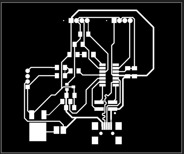
Finally we create a Png file from the Traces layer with traces in white and background in black
Slicing Process
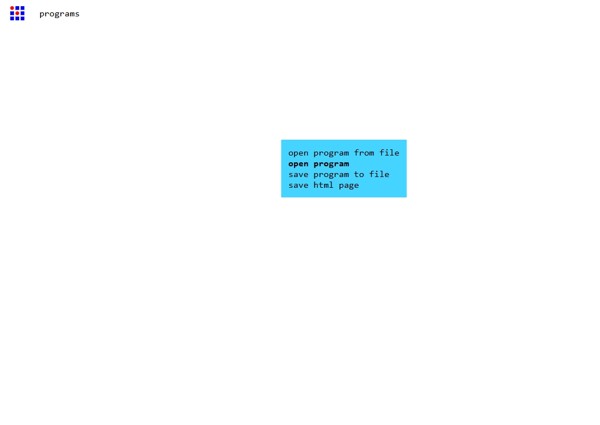
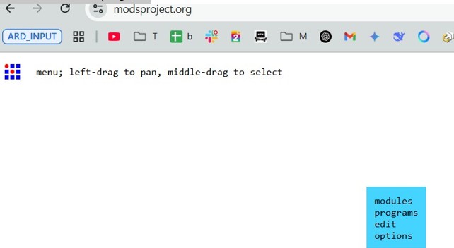
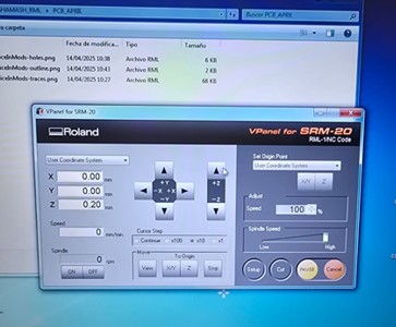
Now we are ready for slicing and go to modsproject.org, then right click and click on 'programs'
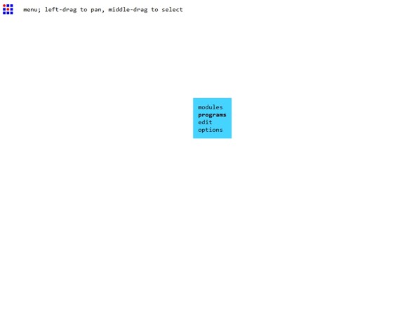
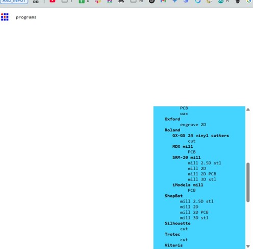
Then click on 'open programs'
Then we choose our specific machine which is an Roland SRM-20
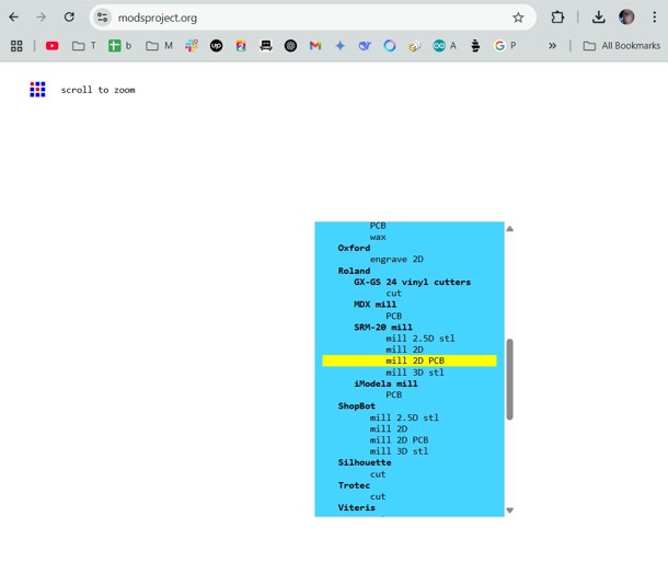
This takes us to the Slice page
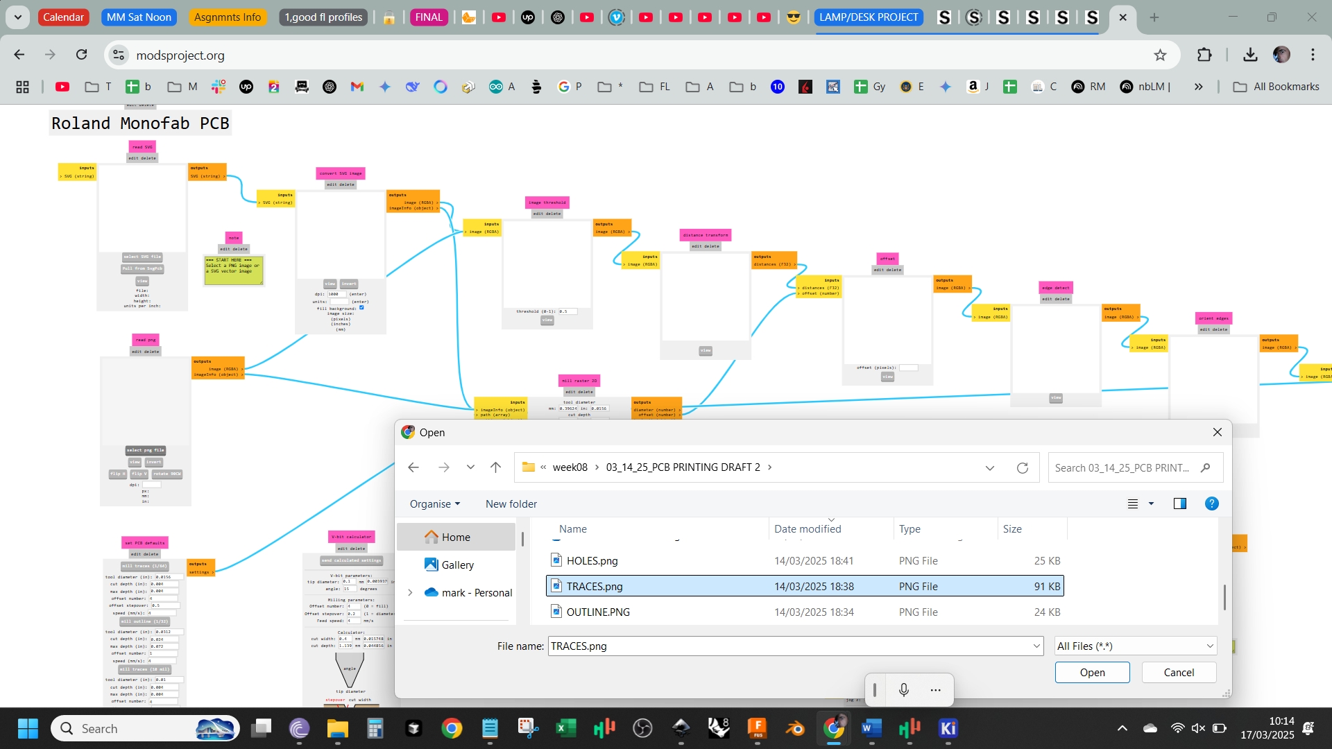
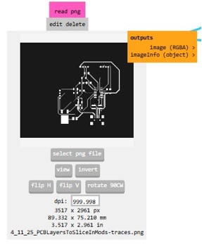
First, we click on 'Select PNG file' and select our chosen file, in my case, 'Traces' from the folder.
The page should look similar to this:
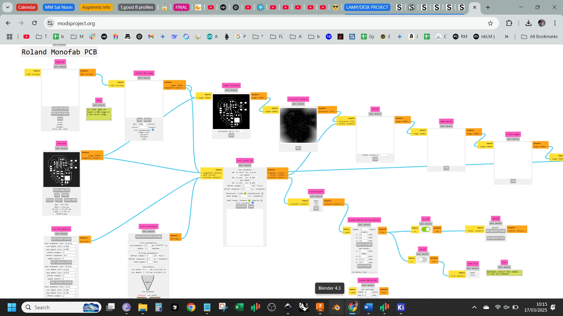
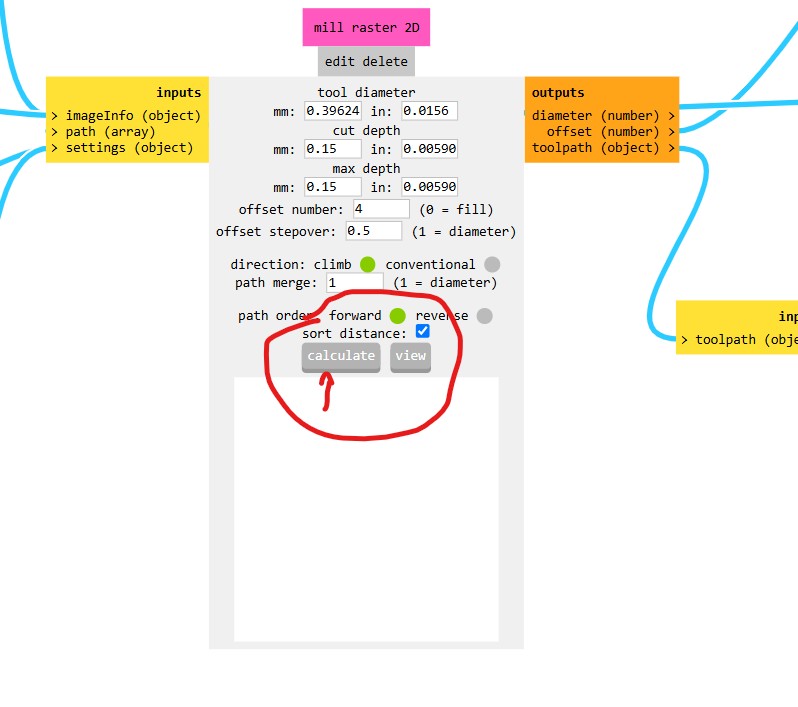
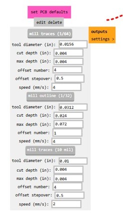
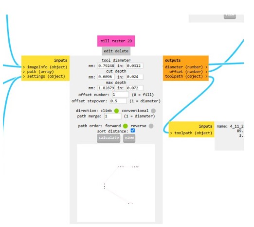
Next we click on 'Mill Traces' so the slicer knows that we will be milling the copper traces
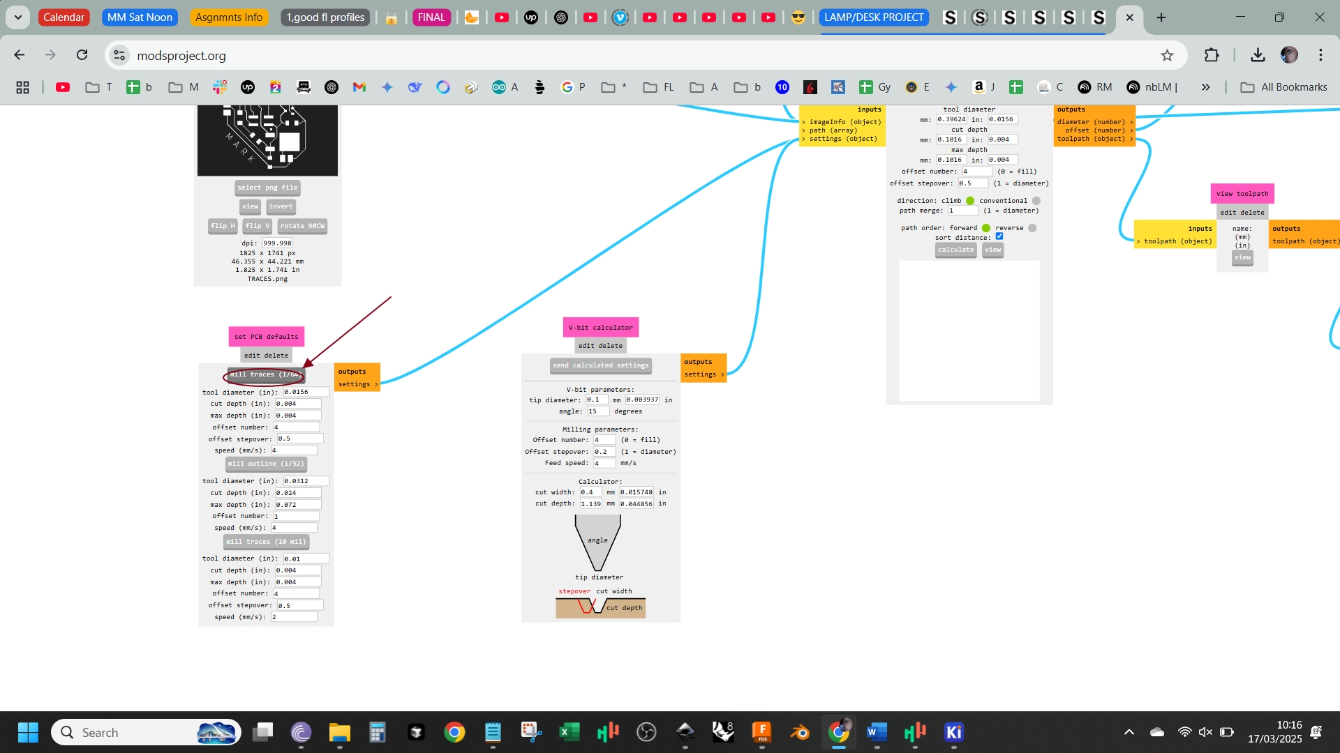
Our 'Mill Raster 2D' setting should have a Cut Depth of 0.15mm and Max Depth of 0.15mm instead of the outline or holes setting of 0.696mm for cut depth and 1.82879mm.
Then we alter the speed setting to 2, and X,Y,Z co-ordinates to 0. Finally we activate the auto-save feature.
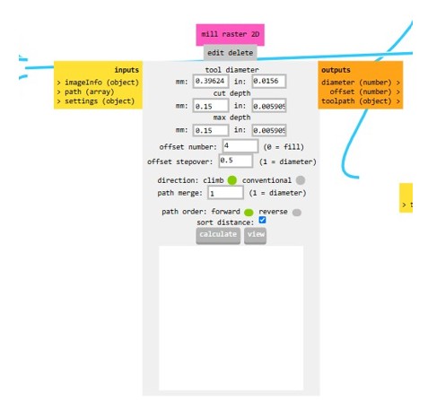
This is how it should look
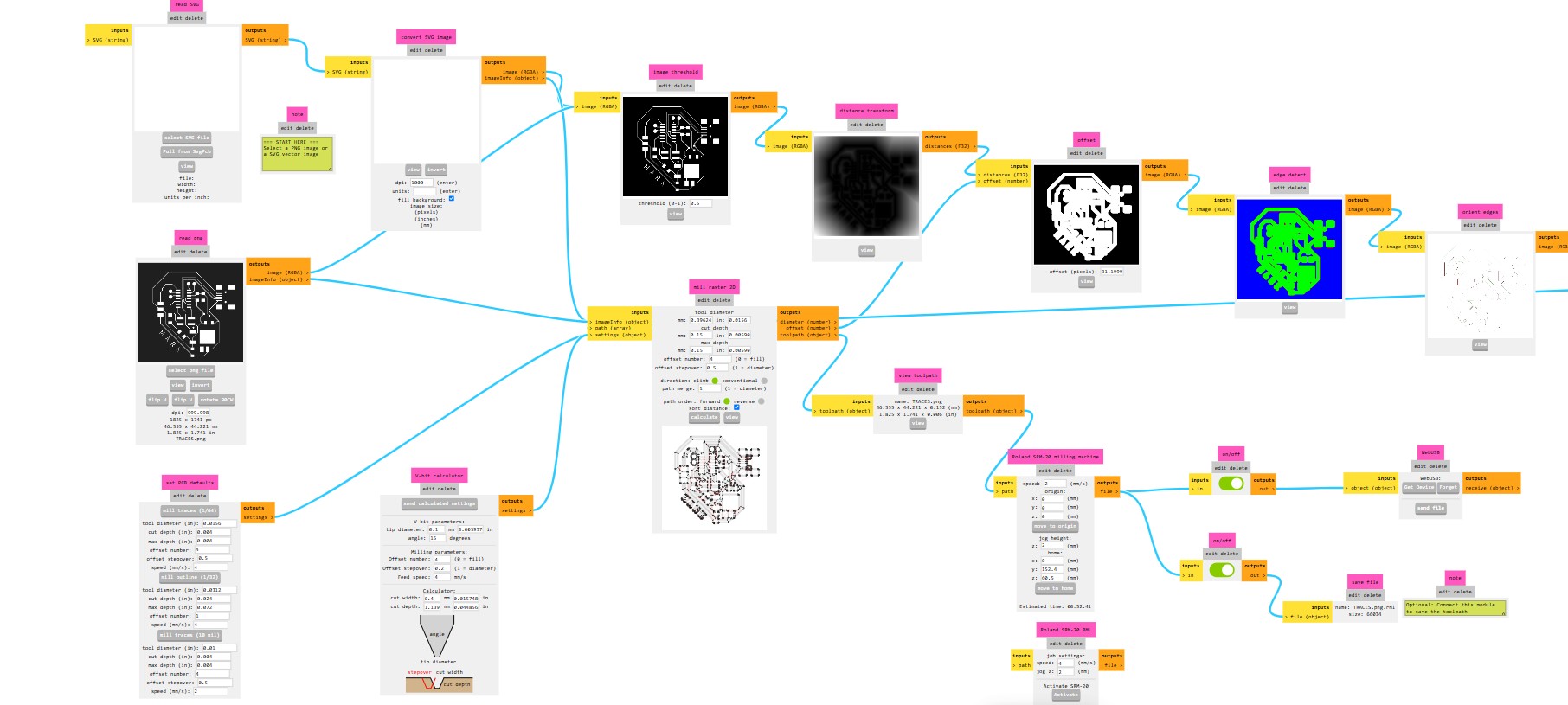
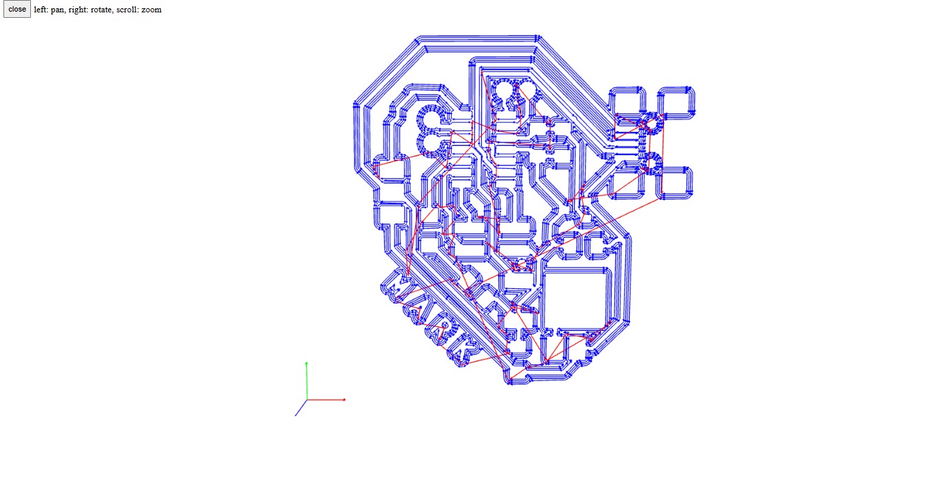
and then we click on Calculate to generate the RML file (sliced file)
This is how the RML should look
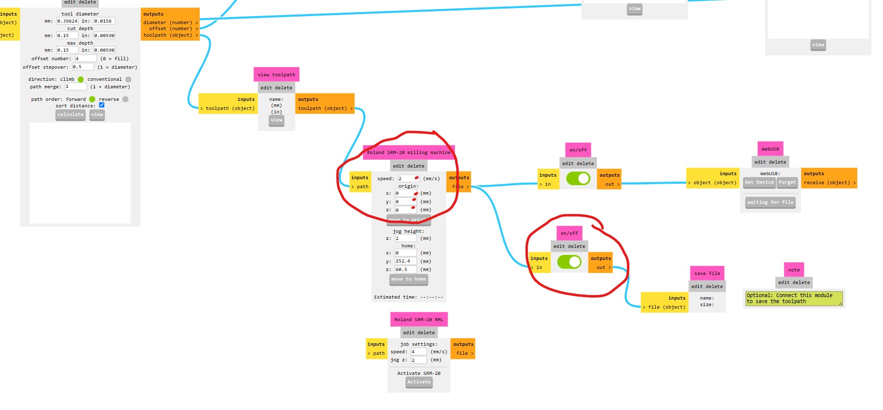
Then we send the three files that we have done for Traces, Outline, and Holes to the SRM-20 PCB Mill and save them to Downloads.
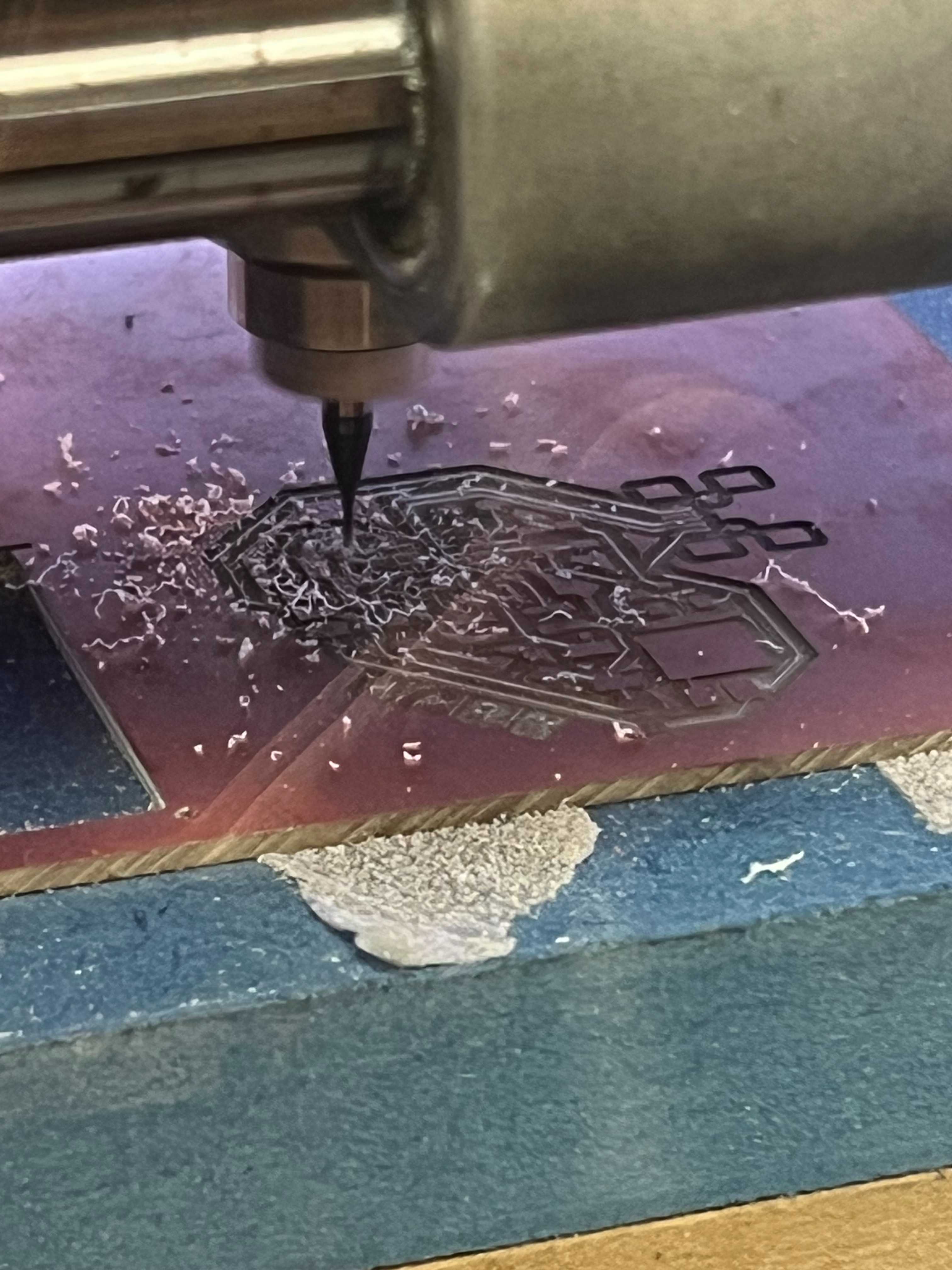
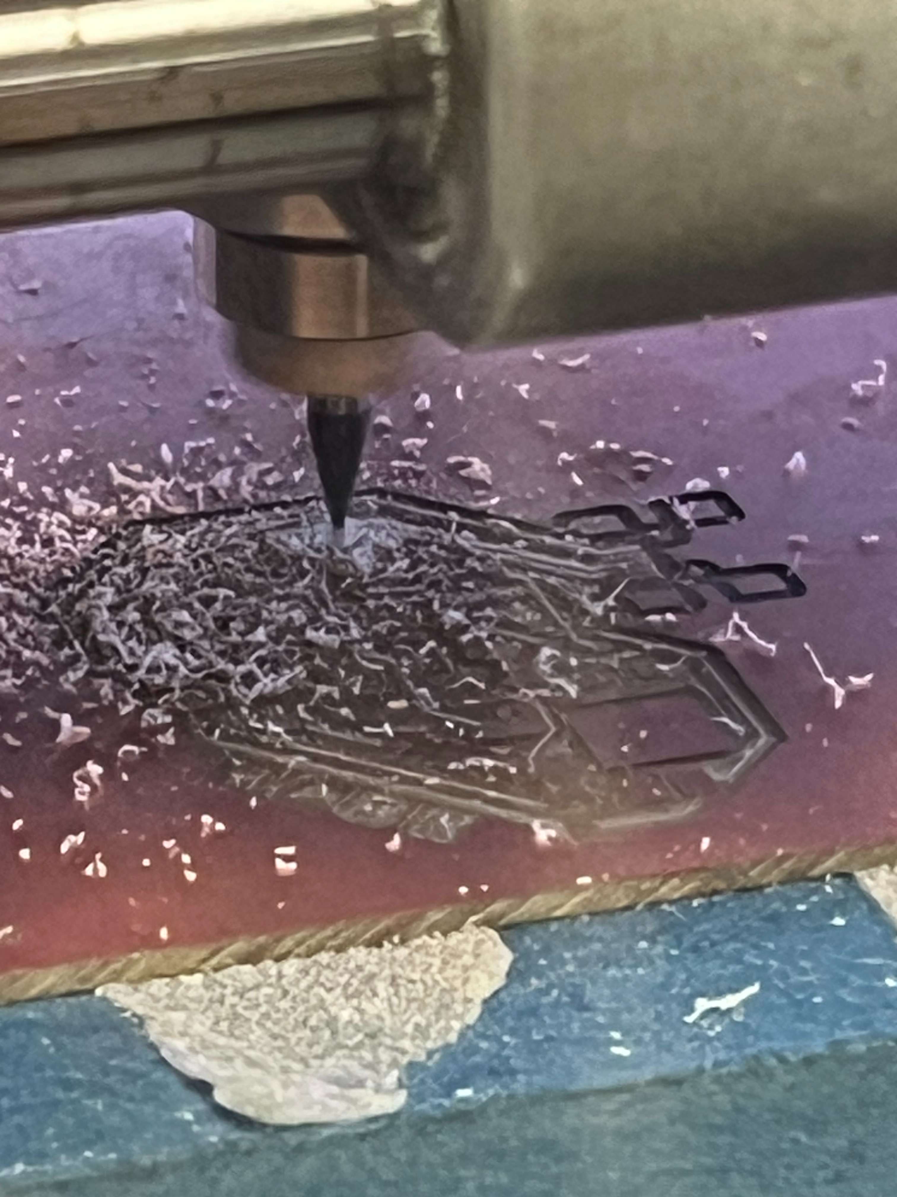
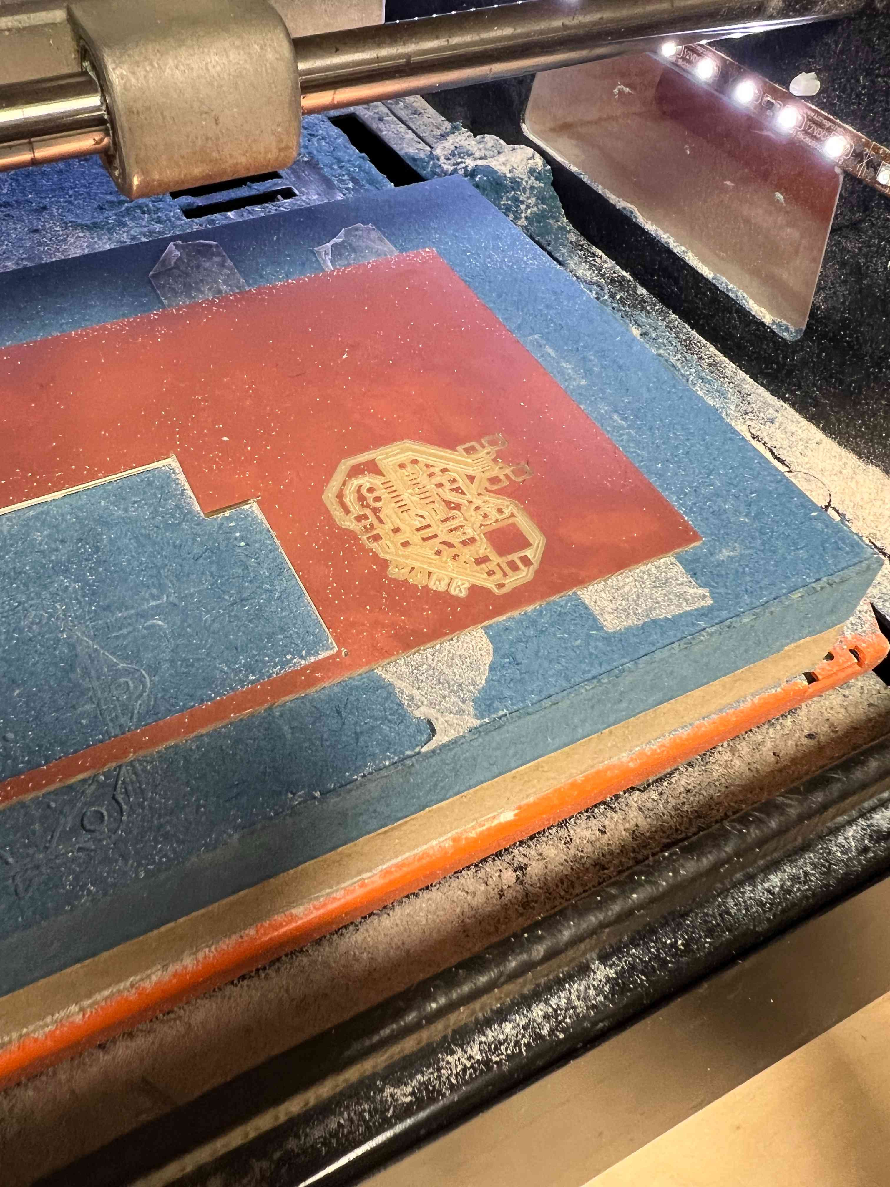
We work on the traces first, then holes and finally the outline. The workflow is intuitive as the traces will have very shallow engraving, then deeper holes will be made and finally an outline will be cut out. We could not do it in another order as any other layer after outline might move around a lot.
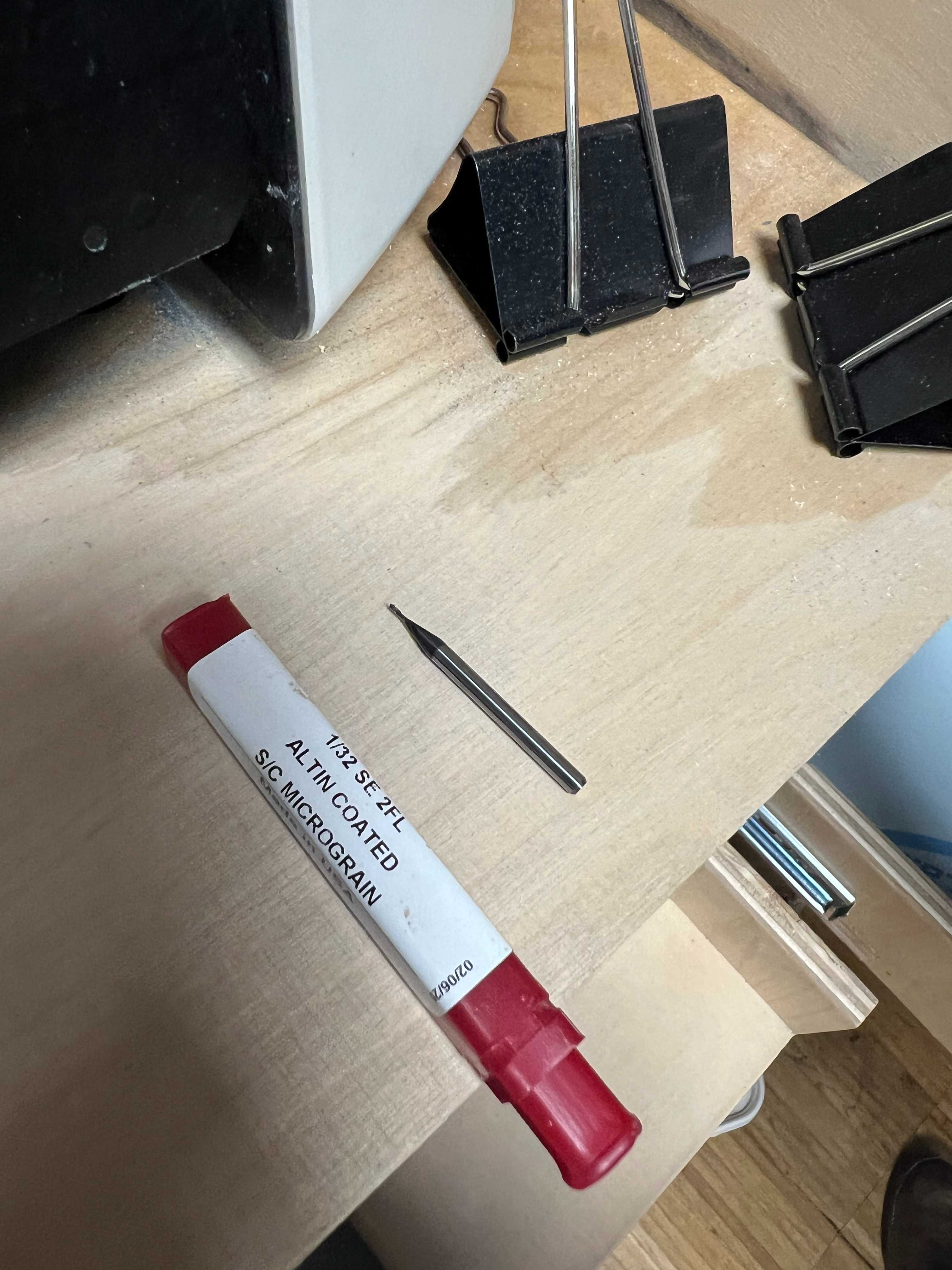
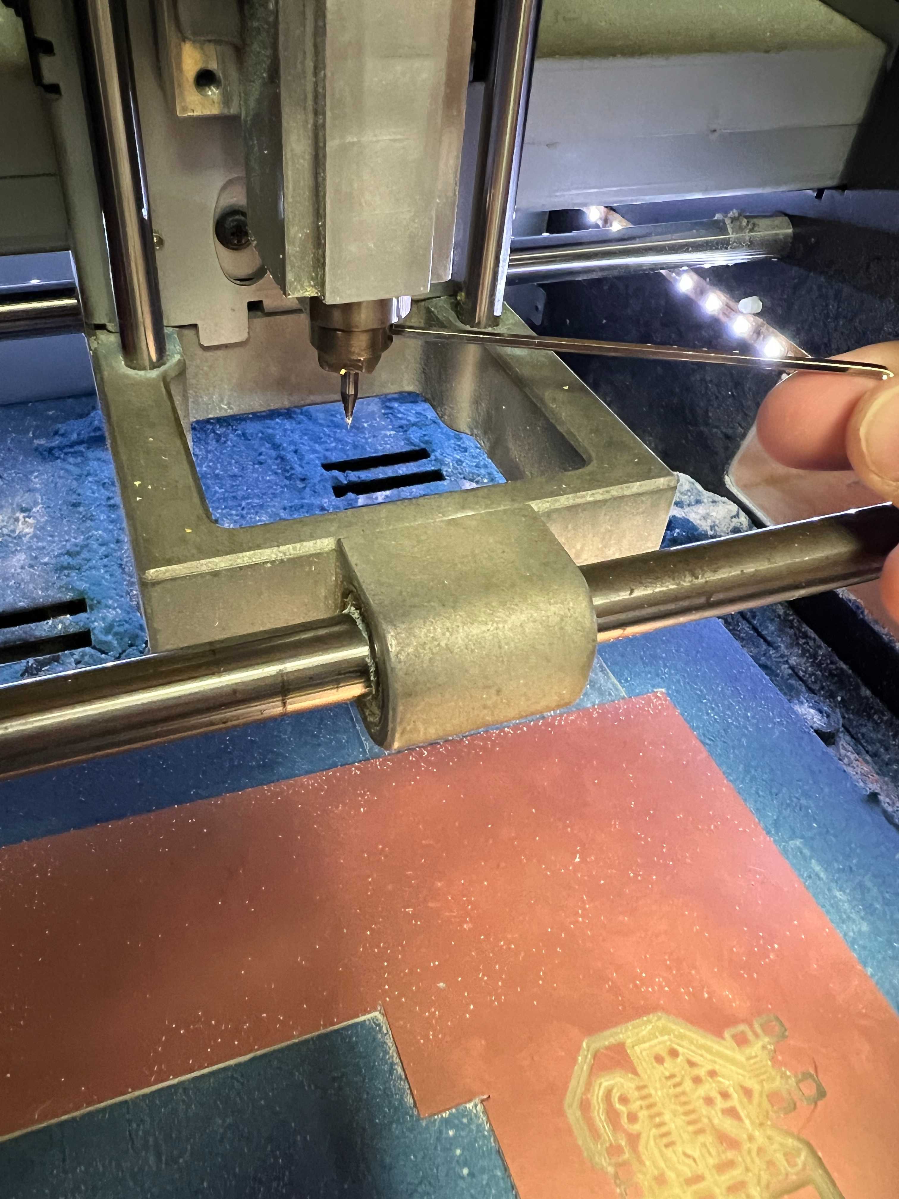
We look for the drill bit that we need. It will be 1/64th mm size for the traces and 1/32th for the holes and outline.
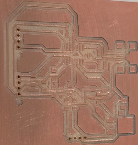
PCB Milling Process
Roland SRM-20 in action milling my chip
Final Results
How it looked when finished
Removing the Endmill to put back in its box
Downloadable Files
- week08HOLES.png
- week08TRACES.png
- week08OUTLINE.PNG
- week08HOLES.png.rml
- week08TRACES.png.rml
- week08OUTLINE.PNG.rml
Individual Assignment - Make and test a microcontroller development board that you designed
This was my first time soldering a board, testing and looking at it closely. 80% of the issue was not having the right magnifying equipment and 20% of the difficulty was identifying what to do.
Firstly I'd like to say that soldering is for me an immensely relaxing and enjoyable process.
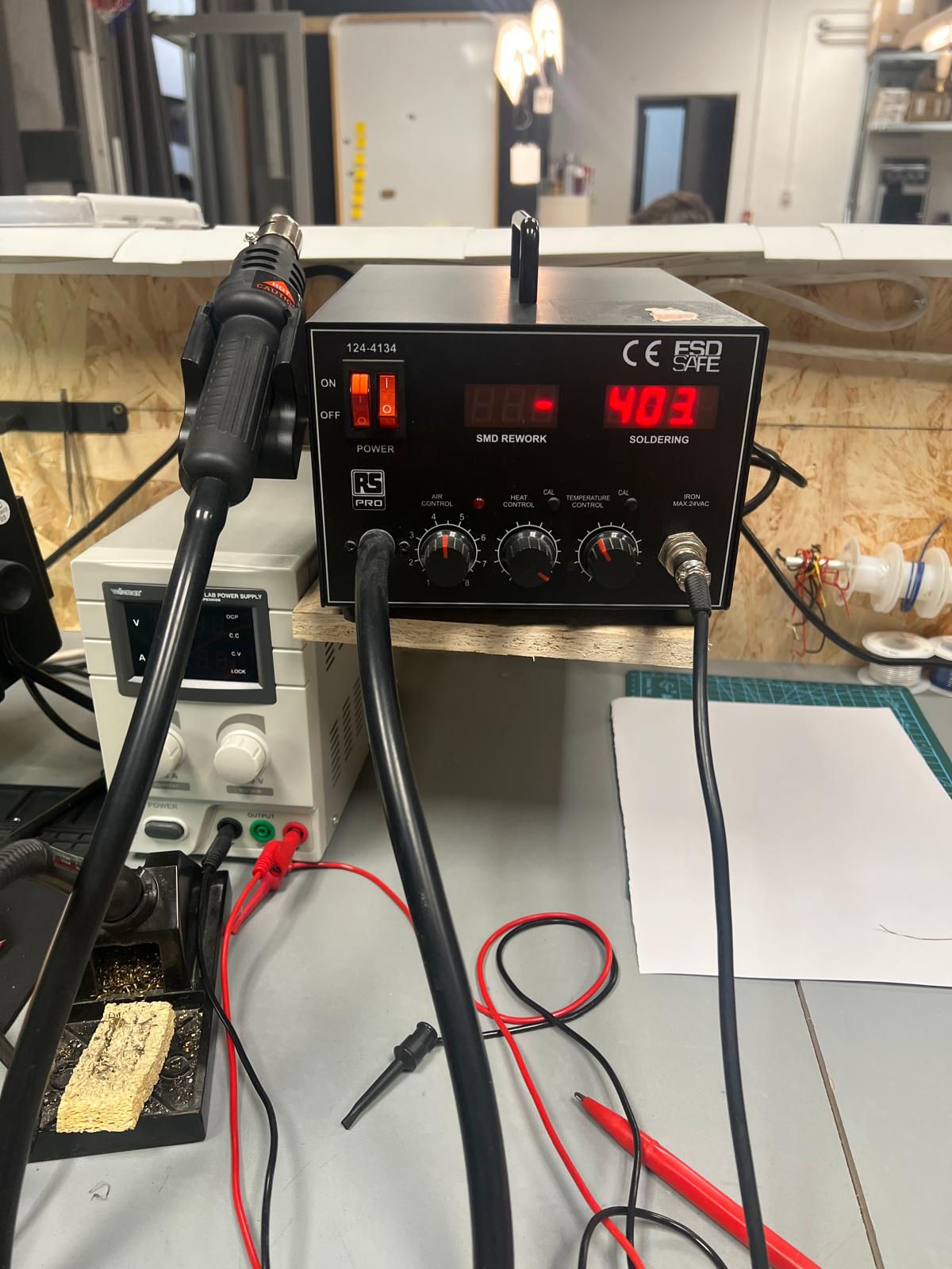
We have our soldering iron which we turn up to a temperature of around 400c
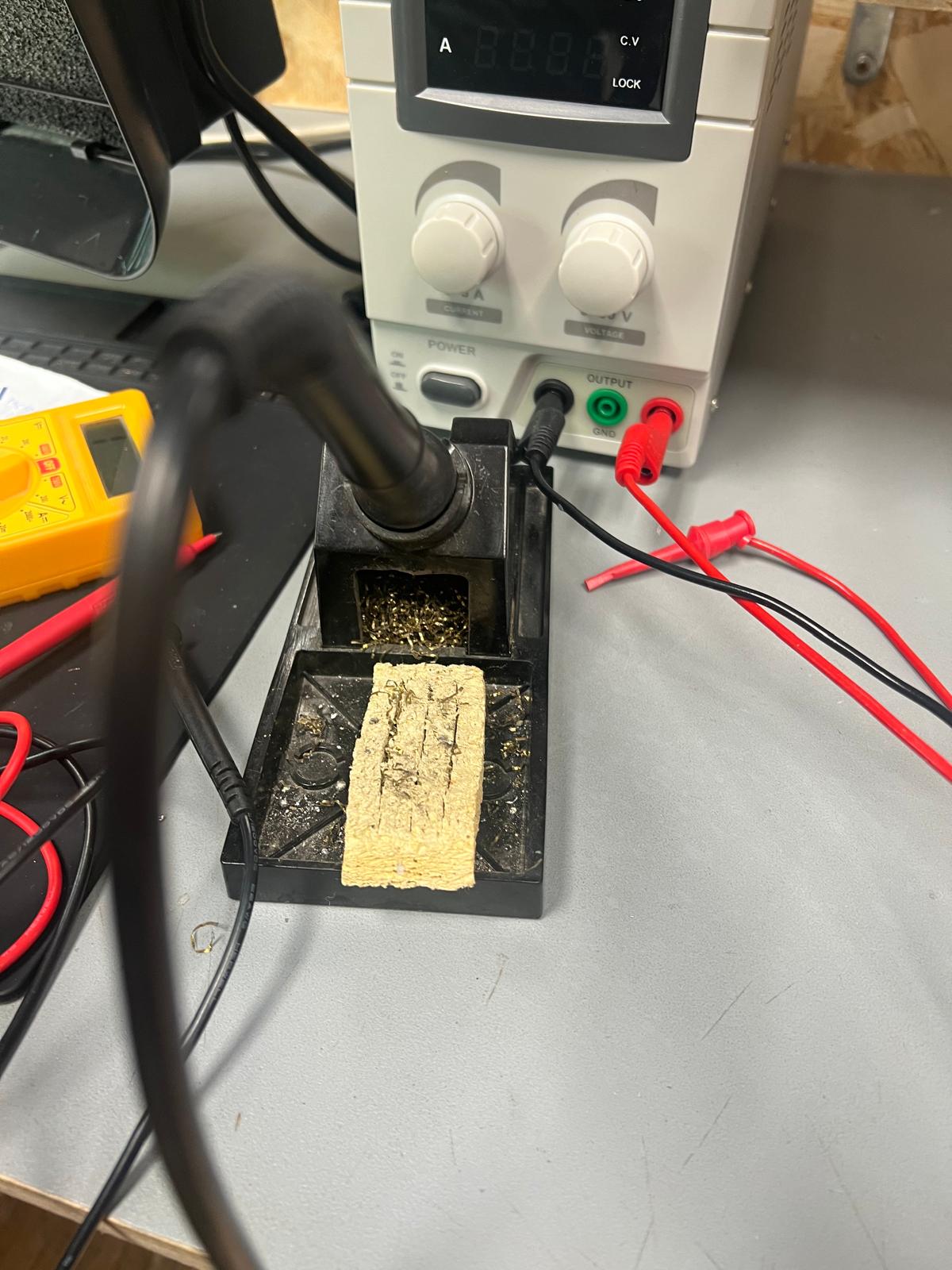
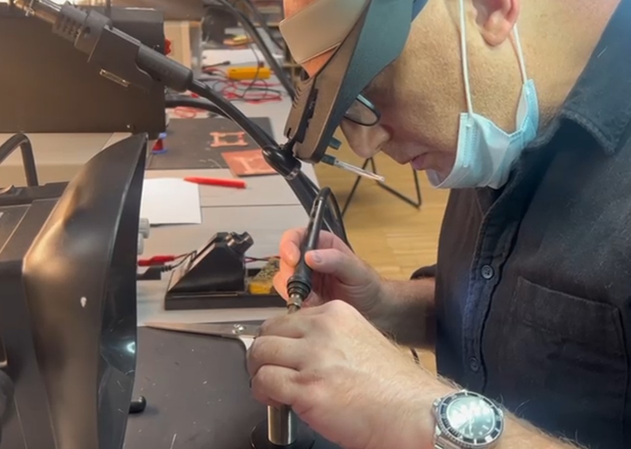
In the second image notice the yellow pad and curly metallic looking material below the soldering iron….we rub the tip of the iron into that metallic looking material to clean it and then press it on to the wetted sponge to make sure the iron is clean and clear.
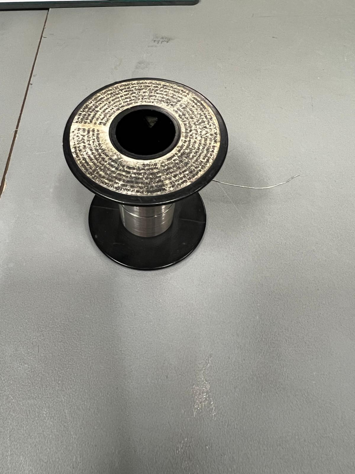
In the picture below can be seen the solder that we use. It is called Rozin solder and is hollow 60% tin and 40% lead. Inside the hollow is flux which is a chemical that helps strip an oxidative layer from the solder so that it can be more malleable and easily attach to the PCB.
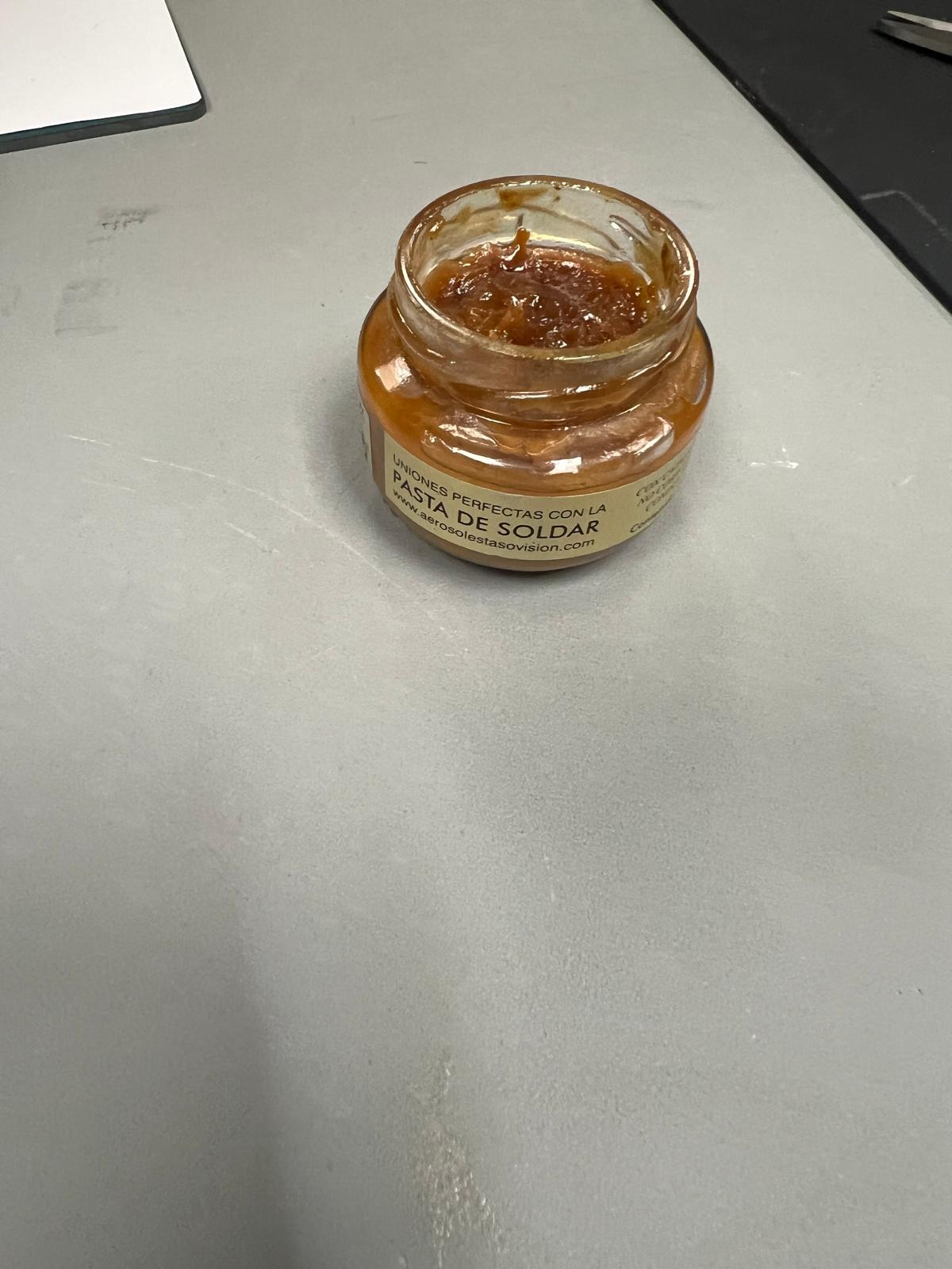
I also like to have some actual flux nearby just in case although I tend not to use it
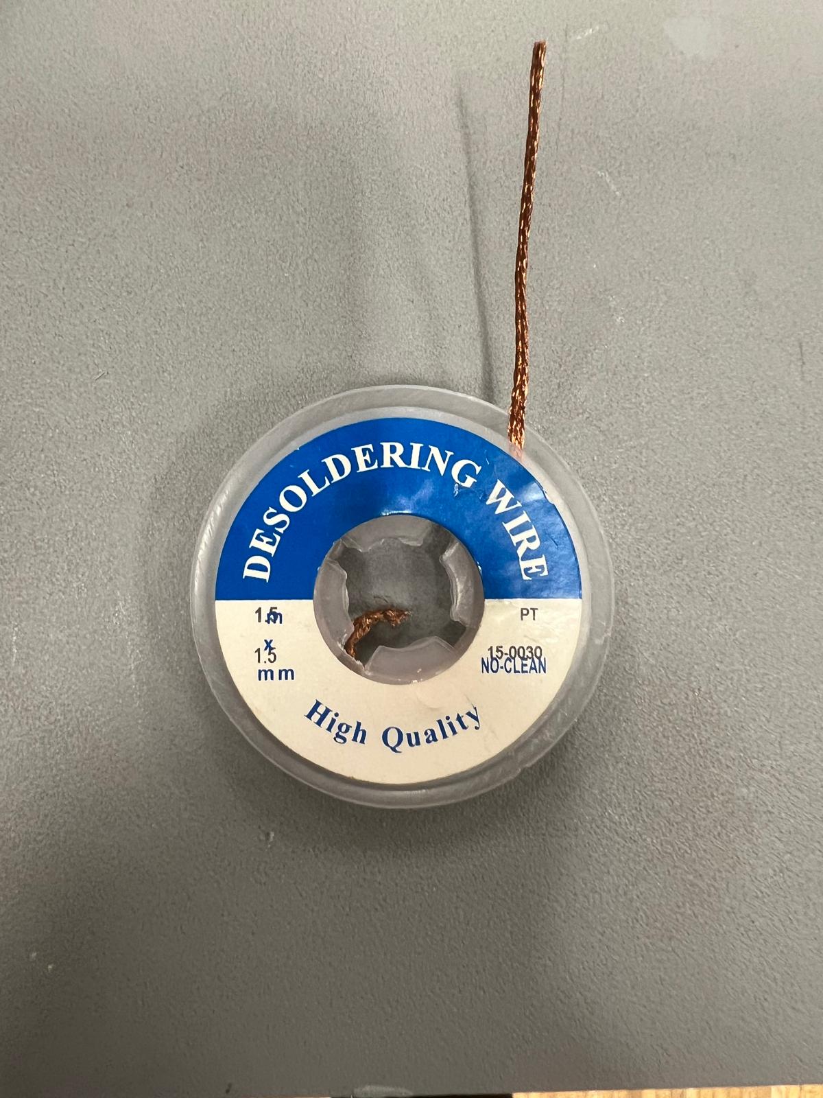
Finally, the incredibly useful desoldering strip which can be seen in the image below. It is very useful if one has applied too much solder and created a short, or one needs to clean up the PCB. I used it a lot!
Another worthy mention is the mini extraction unit which helps to gently suck out all the noxious fumes that are released when soldering. It can be seen to the left of the picture with a shot of me soldering
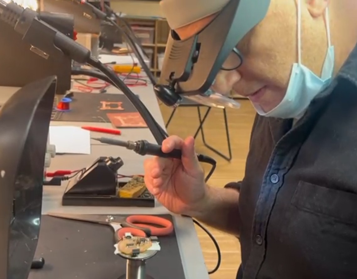
After I completed the soldering Adai sat with me and showed me how to test the PCB with the multimeter. It was my first time doing so and I found it quite hard to see the board perfectly. The explanation was very helpful though I am personally in the 'I feel like I've landed on an alien planet' stage. I am hoping to get much more exposure to this.
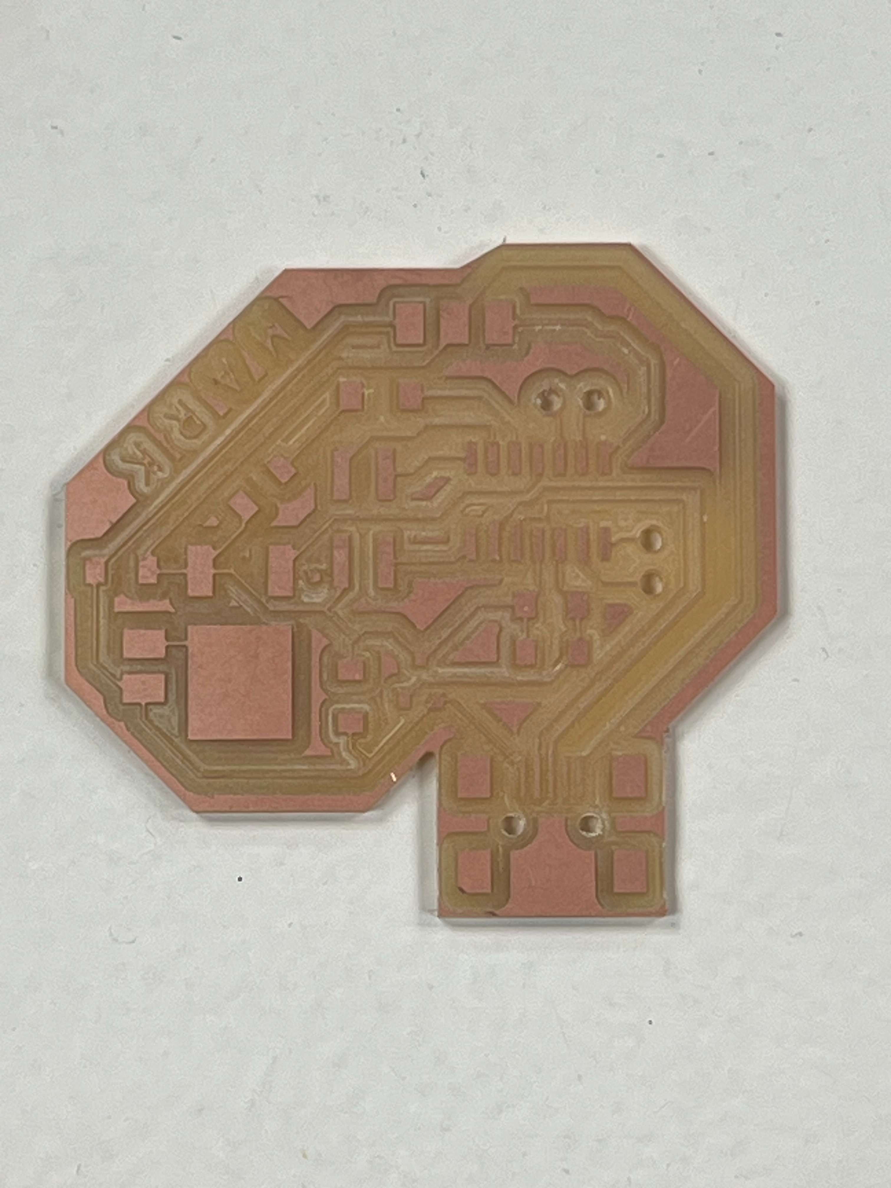
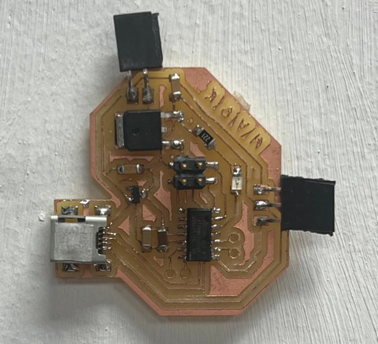
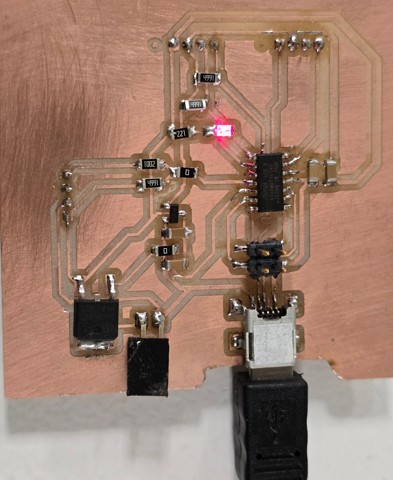
The final chip
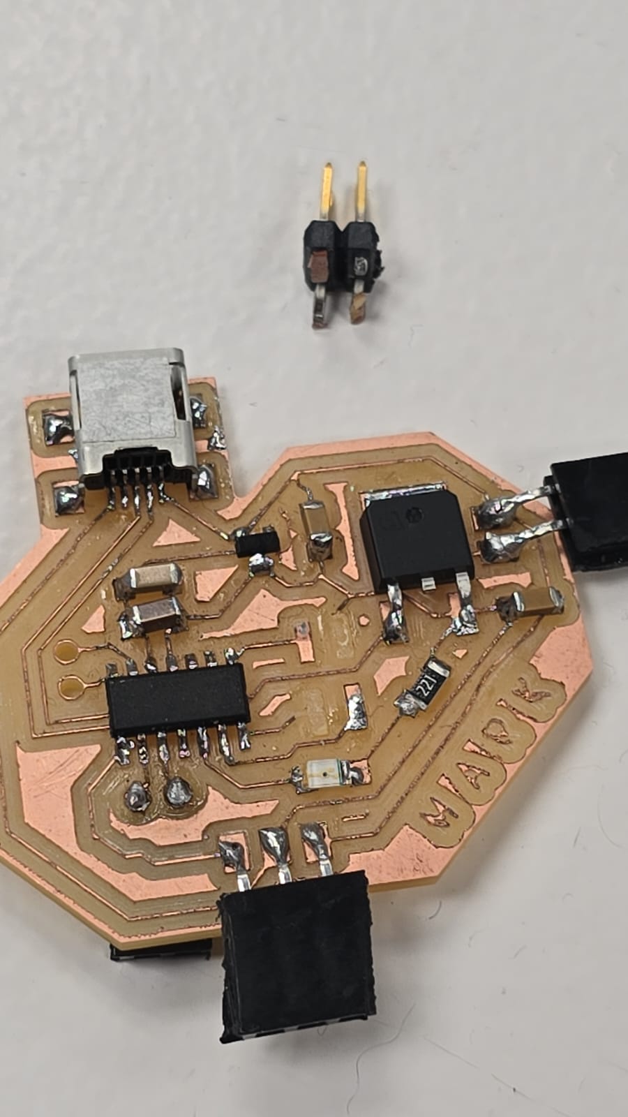
Now I have the final chip I need to flash it for the first time using a bootloader.
Just as I wrote this I realised that I broke off the connector that I needed for this bootloading operation. I have been carrying it around with me for over a week.
I'm quite peeved as I was looking forward to finally being able to do this. If you look closely at the image you can see at the top that broken 4-pin connector and the space missing on the chip
So it turns out that for my final project I will need one or two other connectors on my PCB for a dimmer control, potentiometer control, and enlarging the board before soldering all the components back onto the chip. I will be working on it this weekend and hope to have figured it out - I think i can do it although it takes me a while to process the information and apply it.
APRIL ADDITION - 04/16/25
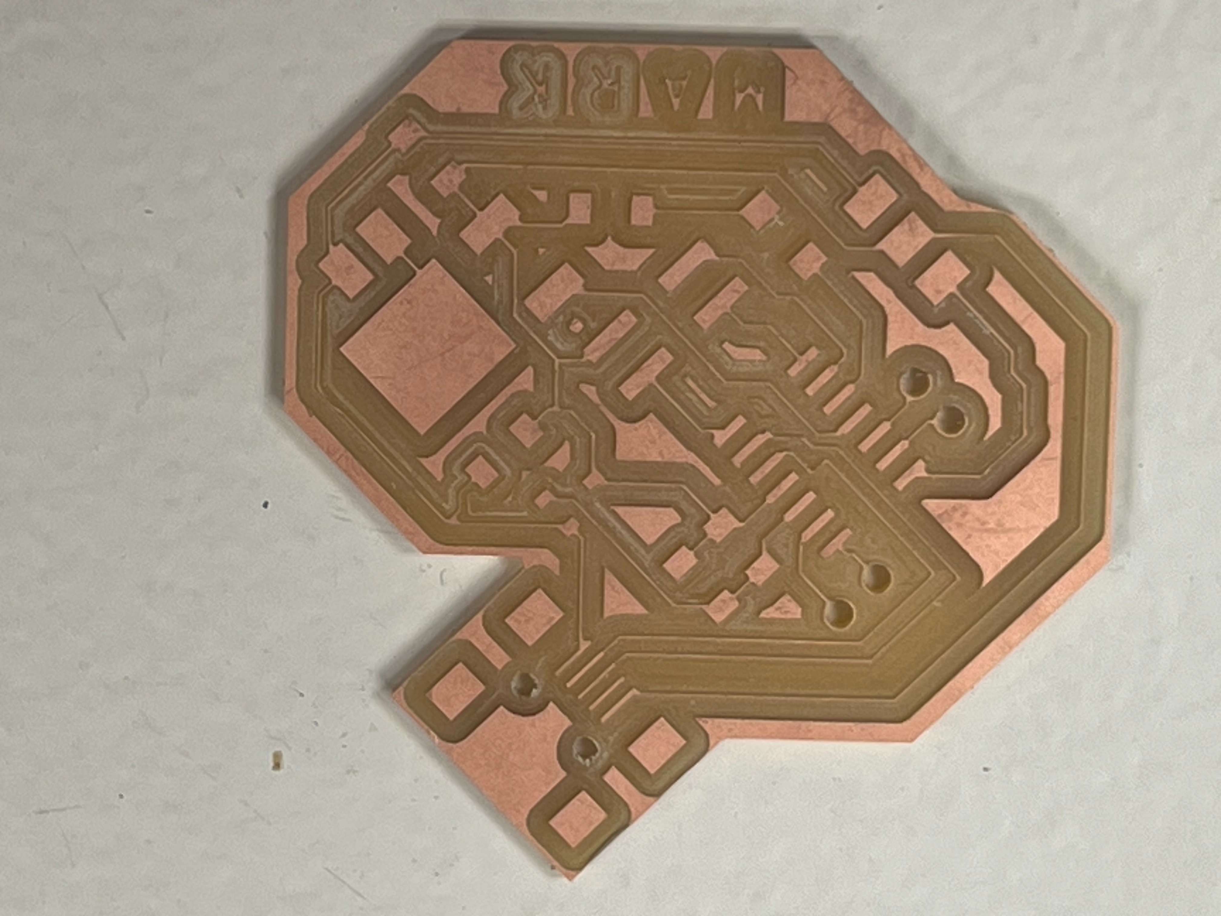
The PCB that I made in March broke and by this time Dani said that I probably should add a slot for Networking and Communications as well as for a potentiometer as a dimmer and a switch for three states, I-0-II (On-Off-PIR), as well as keeping the PIR sensor.
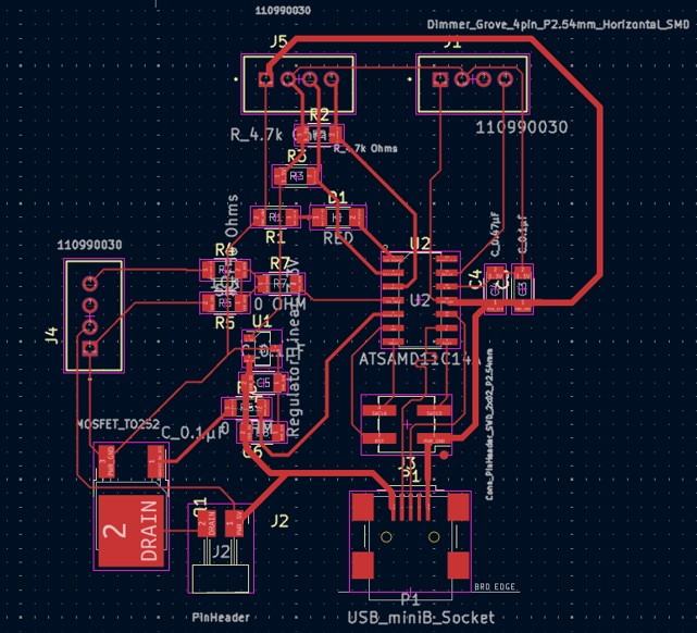
My re-made board
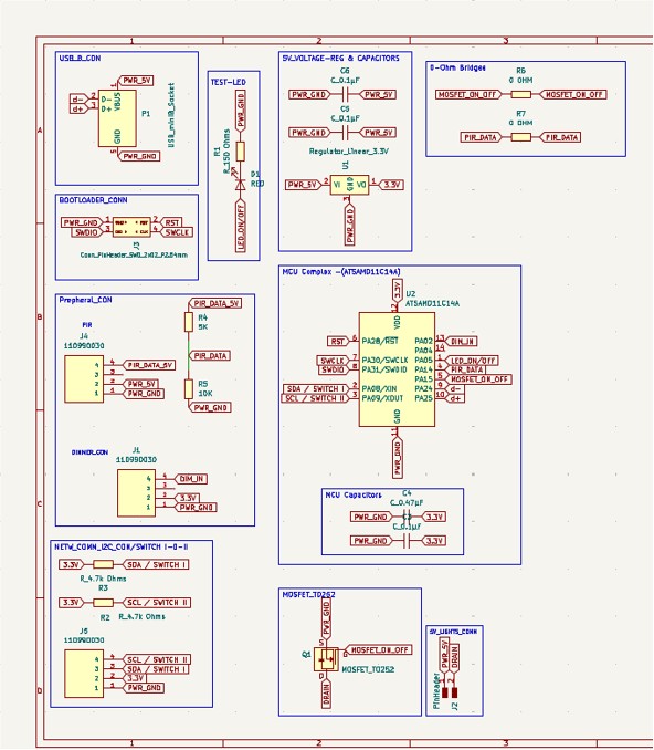
Changes that can be noticed from the first time is that it now looks much more organised with boxes and titles so it is clear what is what and where it is going. This really suits my personality to lay everything out neatly and planned before going further and I recommend it as a time saver in the long run.
A guest appearance was made by the 0-Ohm bridge – this is done on a single layer PCB when crossing wires make it impossible to connect to the desired point. A 0 Ohm resistor is layed and allows the trace to run over it like a bridge.
Another part of my design that needs explanation is the fact that Dani asked me to include communications in my design. It needs a Clock and a Data port connection from the connector to the MCU as did my PIR sensor. I had to use up 4 pins for the PIR and the networking. Additionally I needed to include a switch to include the states of ON-OFF-ON(PIR), and Dani suggested I let that functionality share pins with the Networking part. It means when we do our networking we can write the code for that, and it would execute, but for the final project it will be inactive.
The PIR sensors have a voltage divider because the voltage comes in to them at 5v but needs to be brought down to 3.3v before going into the MCU.
Normally PIR sensors need pull up resistors because their output is typically a low voltage signal when motion is detected and a floating state when no motion is present. The floating state can lead to unreliable readings due to noise or interference and the resistors avoid that issue. In this case the voltage dividers negate the need to use one.
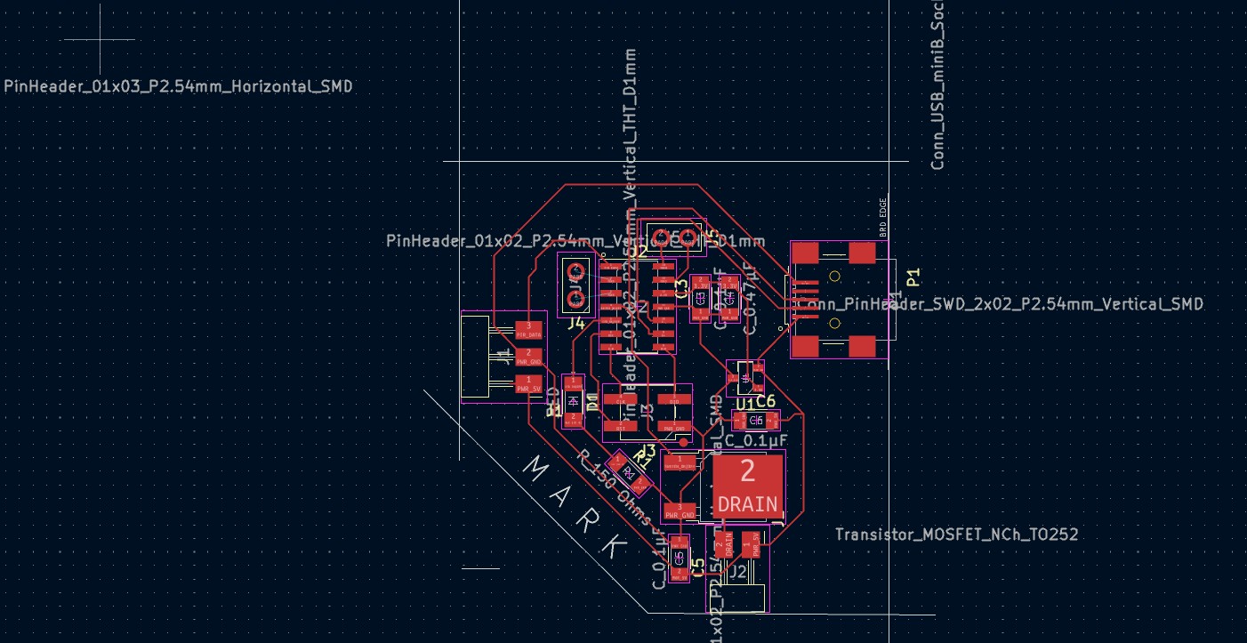
On the PCB design is is easier to see how the 0-Ohm resistors are implemented.
The next step is to create layers in Inkscape for the Holes, Outline and Traces which we will later generate a G-code for and then mill. For me personally, this was the most annoying aspect of this process as I always manage to miss little things. I encourage anyone going through this process to note all steps, even the very small ones. Until one repeats this process enough times it is possible to be absent minded about some little steps.
To export a file to Inkscape and create the layers we Export as a pdf by clicking on Print in the File menu
This exports all the layers into a pdf
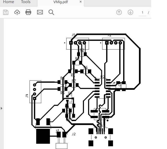
which is opened up inside Inkscape to create layers.
When the pdf is imported you can see on the right handside all the different paths. Each paths represents a different item on the inkscape file. Some are holes, some are traces, some is the outline and some are part of the mask and other variegated. We need to create layers OUTLINE, HOLES, TRACES, as well as Background, and then put each path into the place it belongs.
Once everything is neatly organised we organise WHITE TRACES onto a BLACK background with a background boundary in WHITE and then save as PNG.
The next is to create a HOLES.png which is BLACK holes on a WHITE background

Finally an OUTLINE.png layer which is WHITE outline on a BLACK Background

It is important to note that the files are to be exported as PNG not 'saved as' and the DPI needs to be set at 1000. Then the file is exported. The resulting PNGs are put through the MODS G-code toolpath generator to create the final printing files which are .png.rml files.
Go modsproject.org to generate the G-code. Right Click then Programs
then click on Open Program
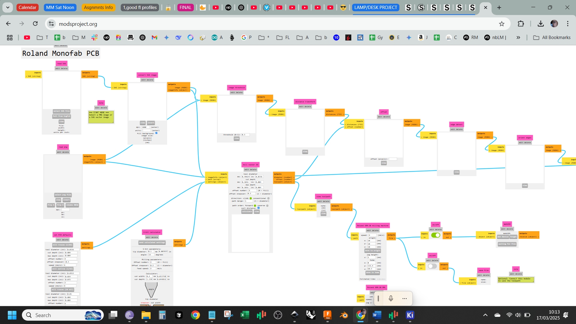
Then click on our mill which is the SRM-20 Mill and mill 2d PCB
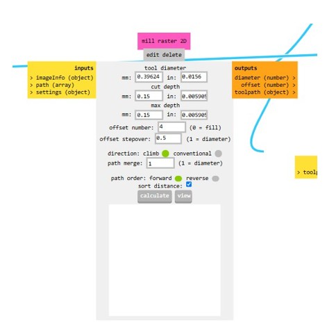
This is what you should see
Select Png traces file first to upload
Click on mill traces
Change the cut depth and max depth to 0.15mm
Change speed to 2 and set x,y & z to 0. Also switch on the Edit delete button below which autosaves.
Then press the calculate button to generate the toolpath code.
This is what it should look like
Now when we do the holes and outlines we click on mill outline and leave default
This is how it might look
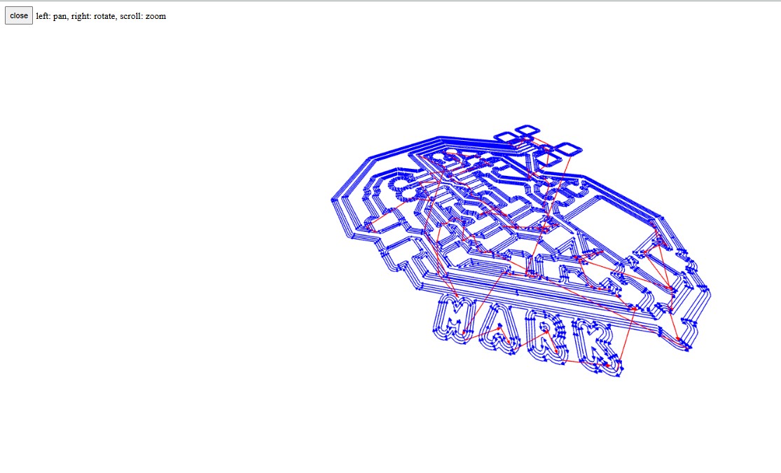
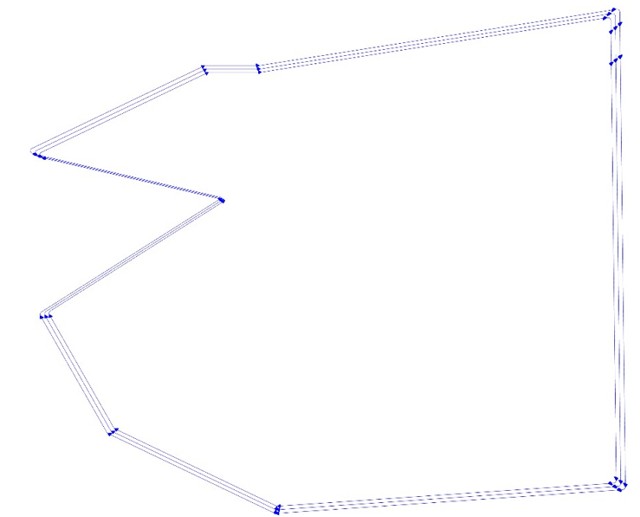
This is how the generated tool path might look
This is an outline I did which I have since retired
This is how the corresponding tool path looked
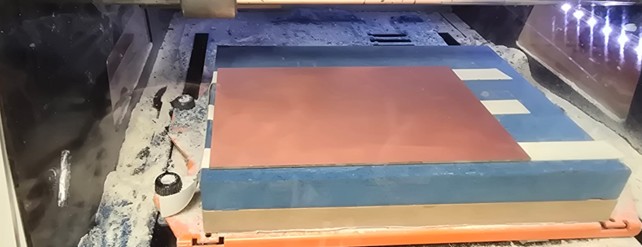
Next we are going to mill our PCB.
- We put our mods files onto the Roland PCB Mill downloads folder not just onto the USB stick.
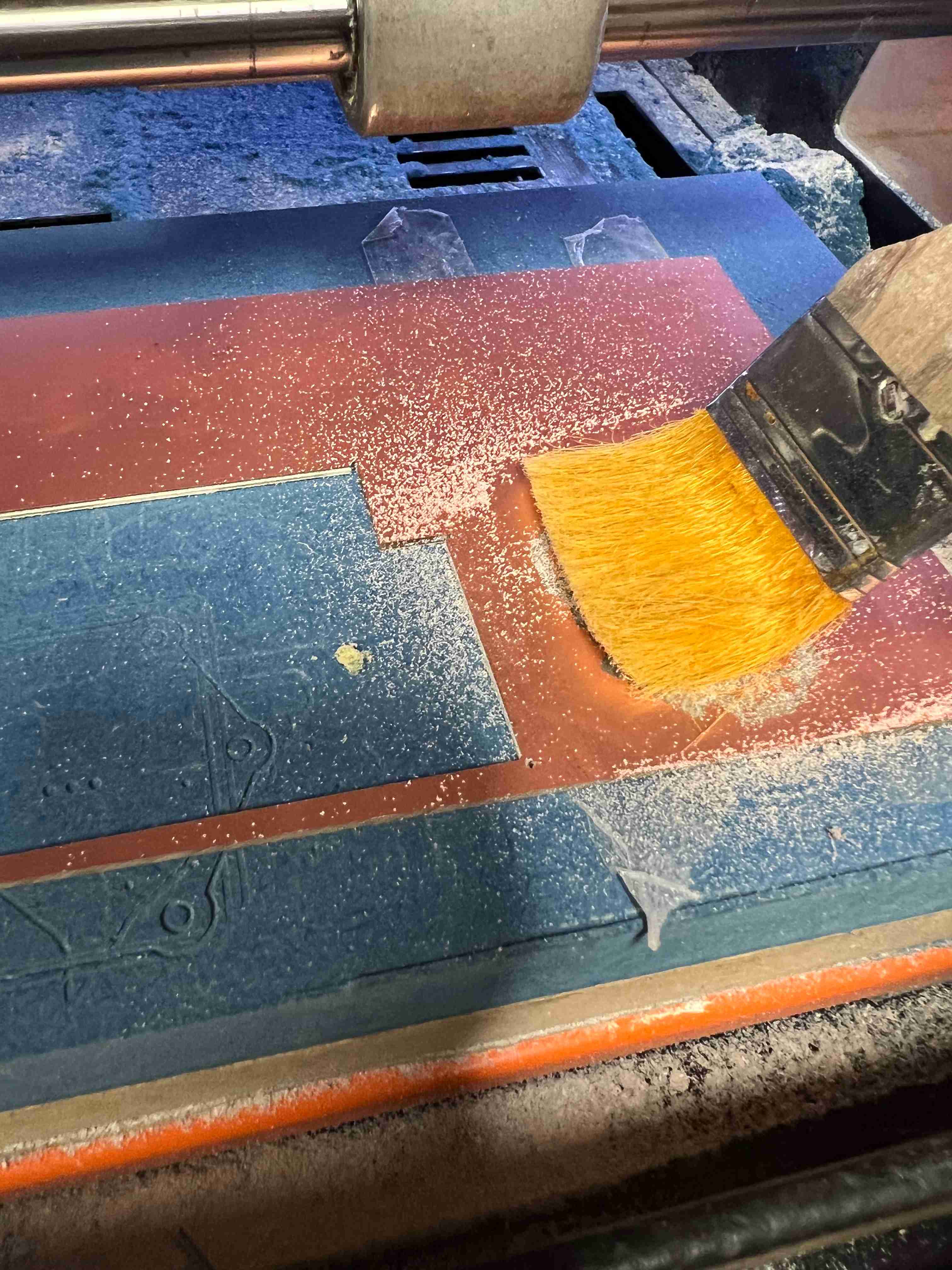
- Clean the bed of the mill with the brush.
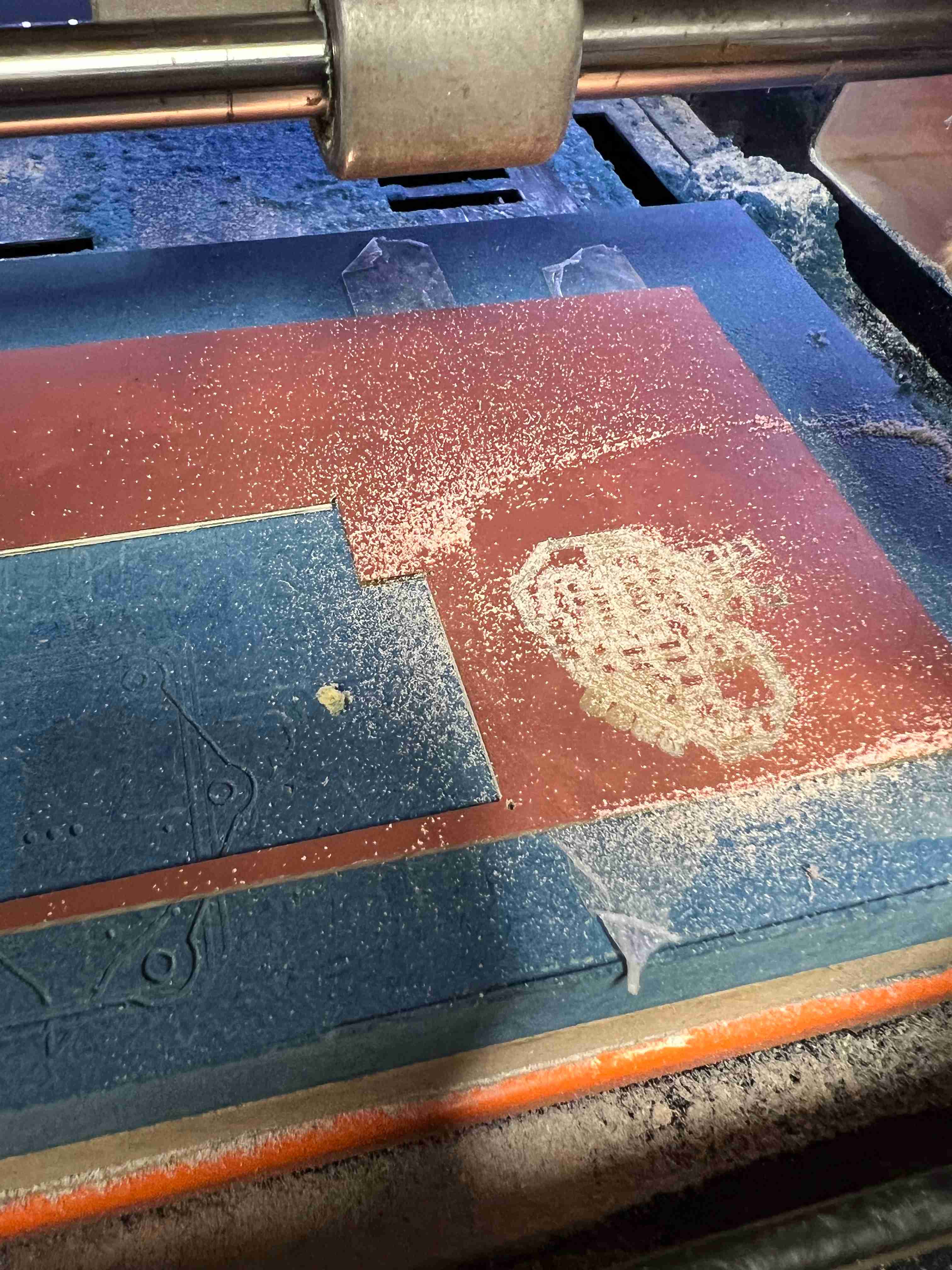
- Attach double sided tape to the back of a 1layer copper and press the PCB down onto the bed – make extremely sure that there are no gaps between the bed and the PCB and that it is pressed down very firmly. Otherwise later on it could produce inexact results. An overly shallow cut or an overly deep cut will render the board unfit for purpose.
- With the Alan key attached to the magnet on the inside of the machine, check to see that the end mill is the required size, i.e. 1.64th for traces and 1/32th for Holes or Outline.
- Insert the correct endmill into the collet, screw it in tight and and bring the end mill close to the copper layer. Then, loosen the end mill again until it drops to the bed. Then, re-tighten it into place. This is to prevent breaking an end mill by crashing it into the copper layer.
- Once the endmill is touching the copper layer zero the XY and Z co-ordinates, and then lift the Z co-ordinate by 0.20mm. In anycase when the printing starts the machine will lift up the end mill and then bring it back down, but this is just a procedure to be extra careful.
- Now press the CUT button. At that point if there are any file names in the area they should be deleted. Then, load into the area the TRACES outline first as this is what we shall cut initially. Then press OUTPUT. The mill will start cutting and it should leave a powdery trail if it is cutting properly.
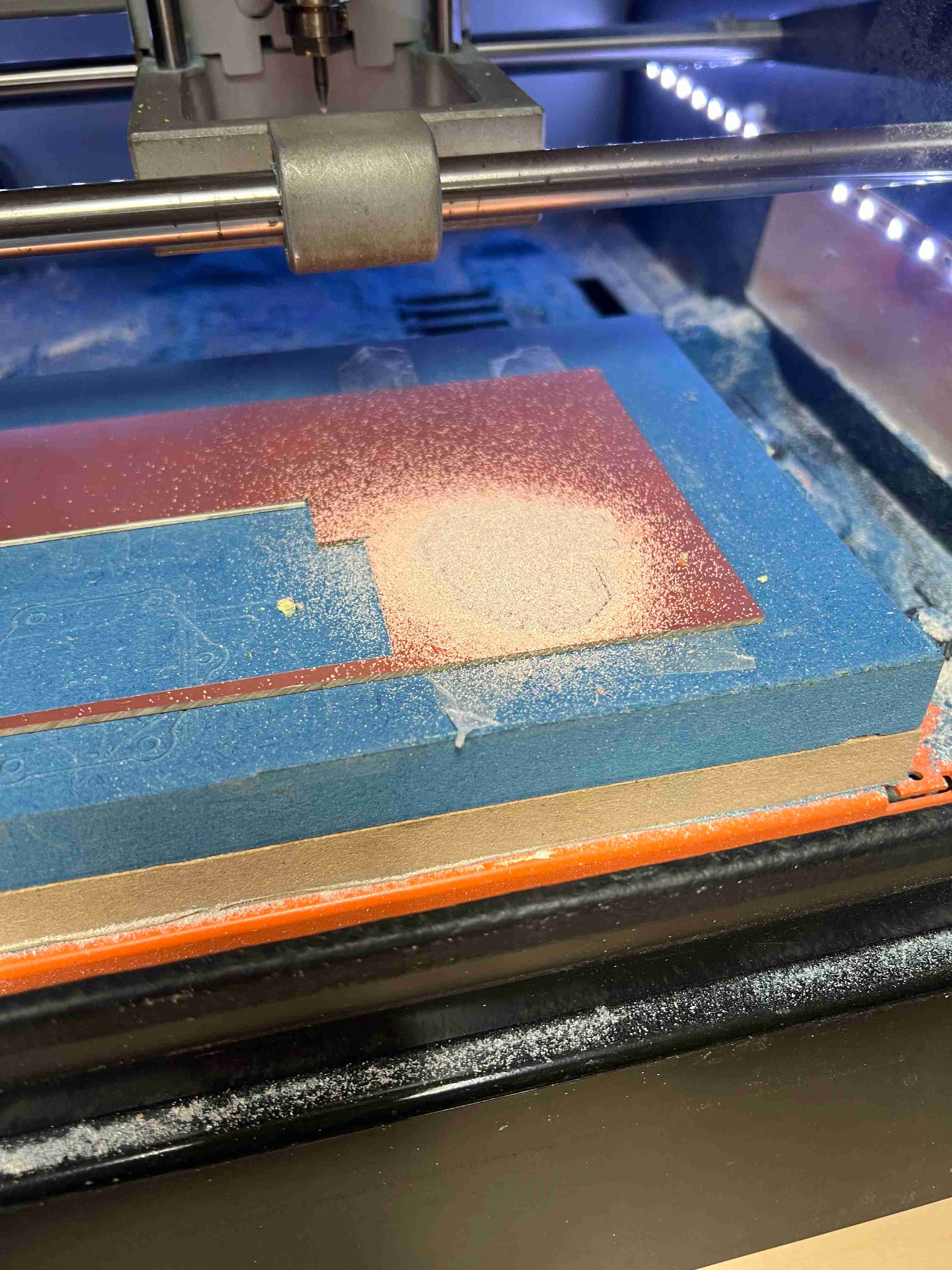
- Once it is finished, replace the end mill with the 1/32th bit for the Holes and Outline. Goto CUT and replace the Traces file with the Holes and Outline file and press OUTPUT.
The result
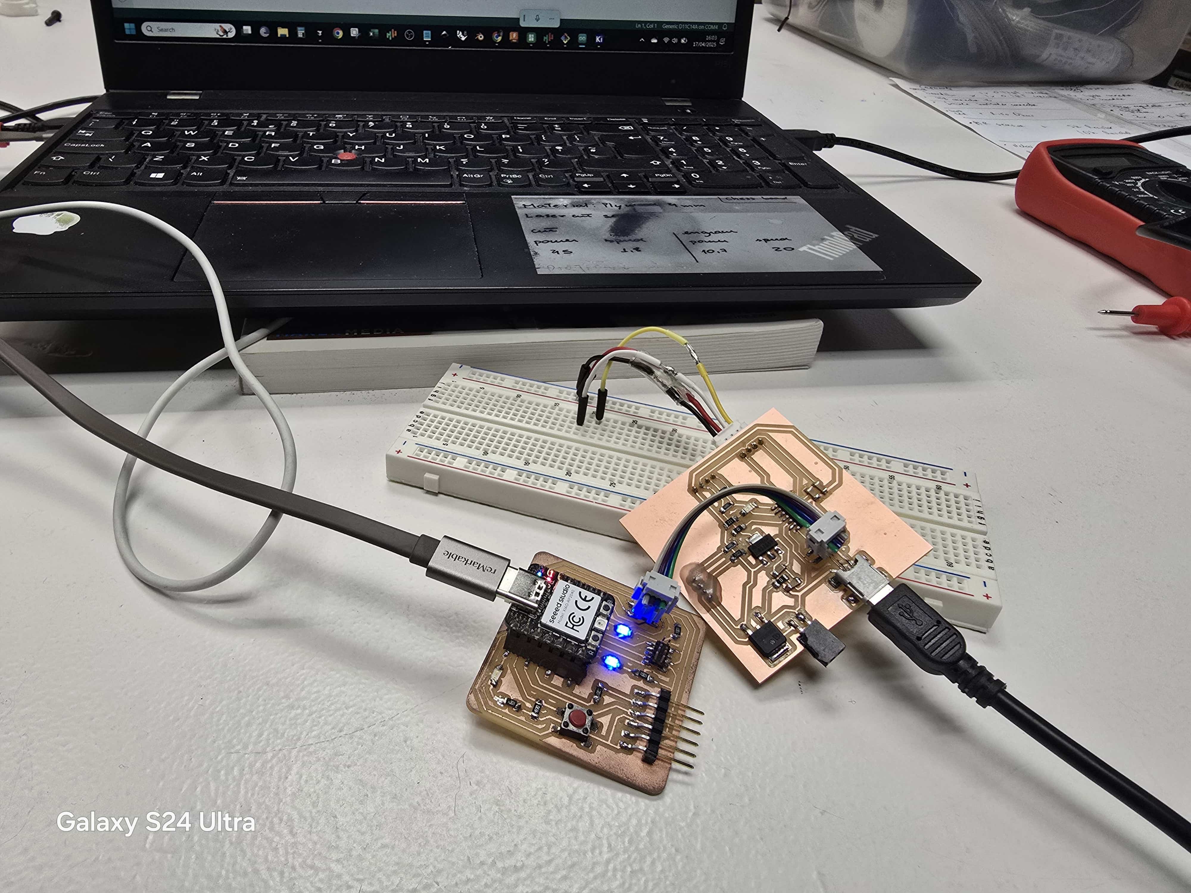
Connecting board pre-flash, LED working
Bootloading Process
First connect the SWD programmer
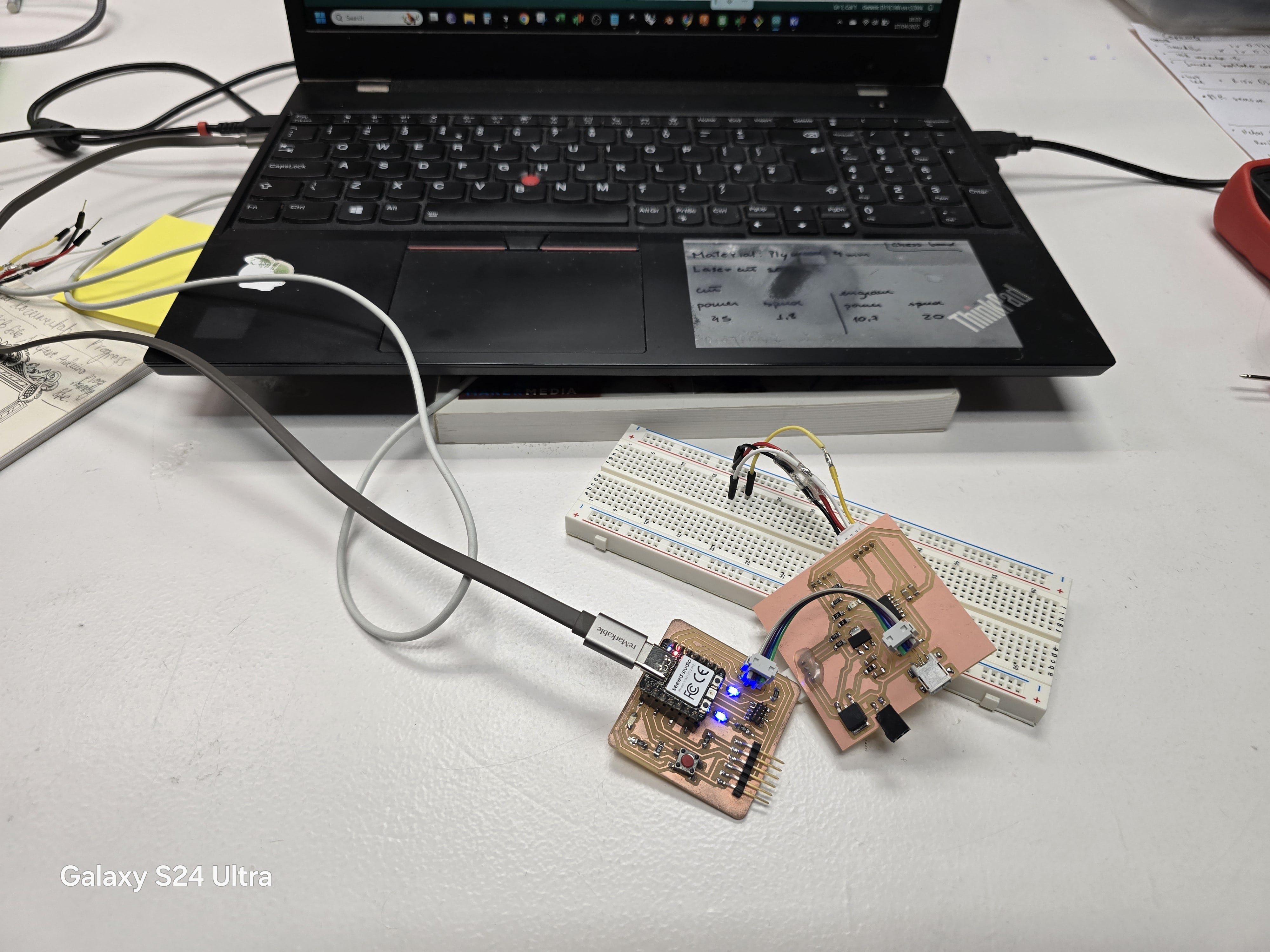
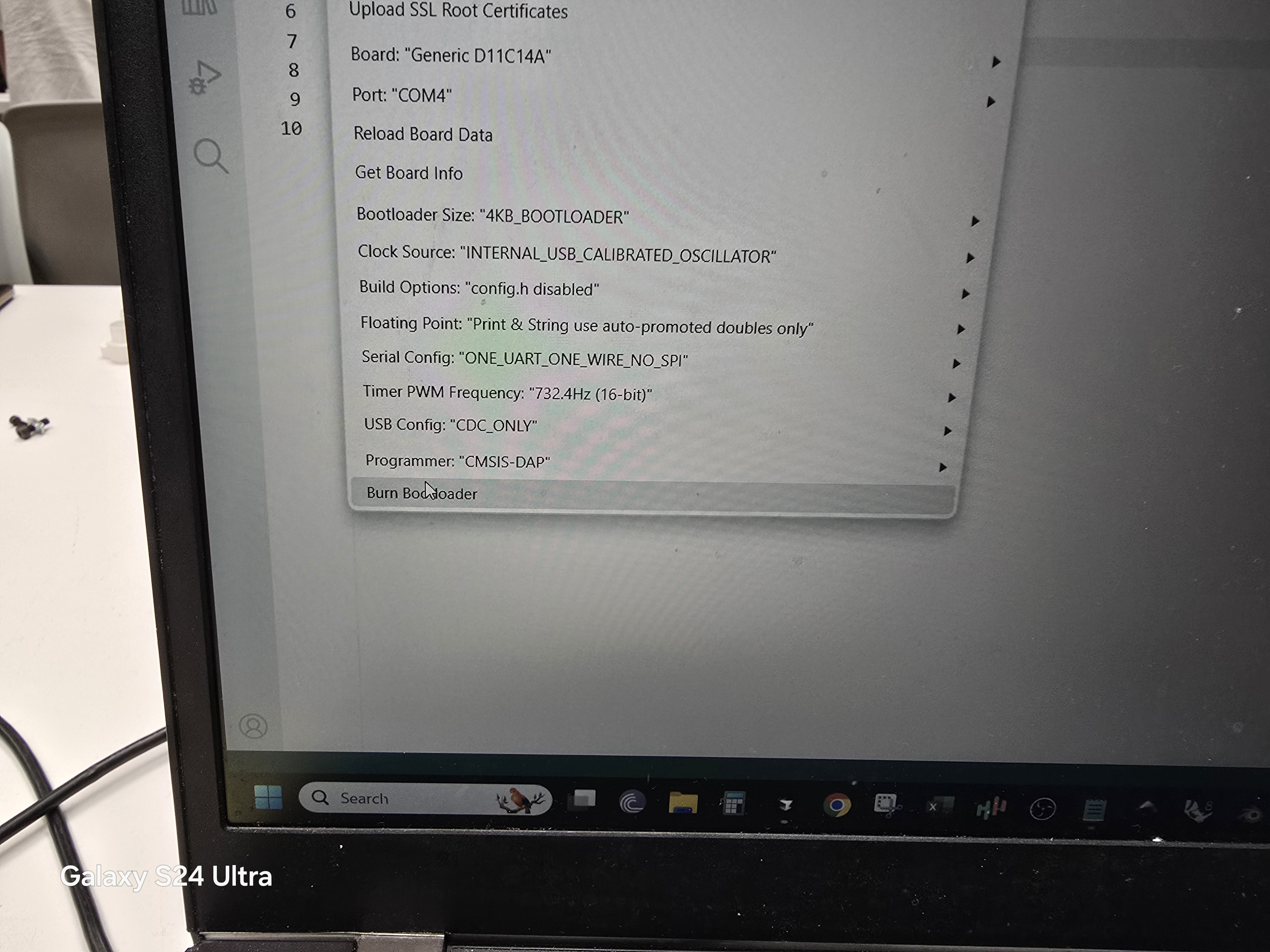
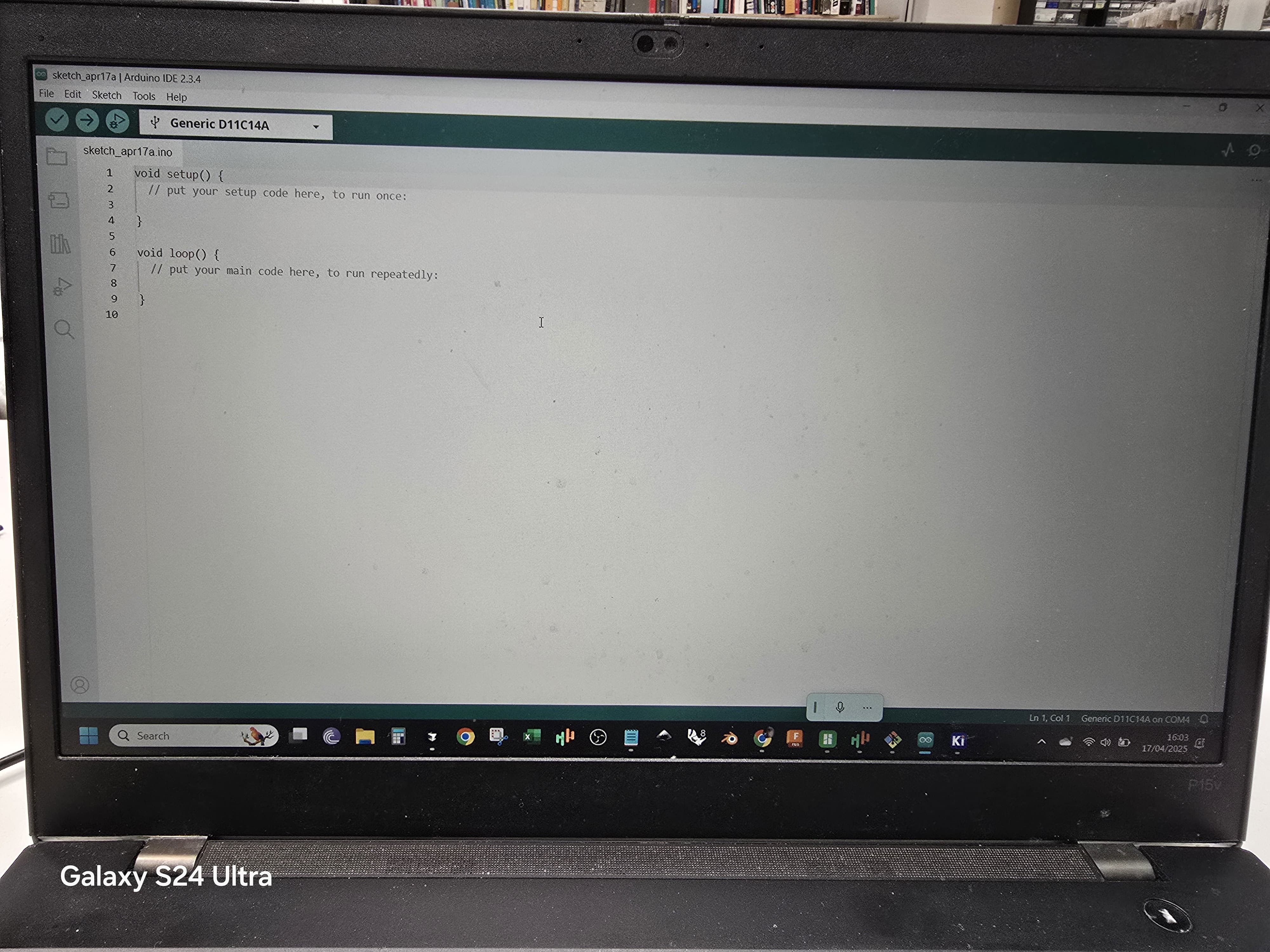
Then make sure that the board that the Arduino IDE is referencing is the SAMD11c
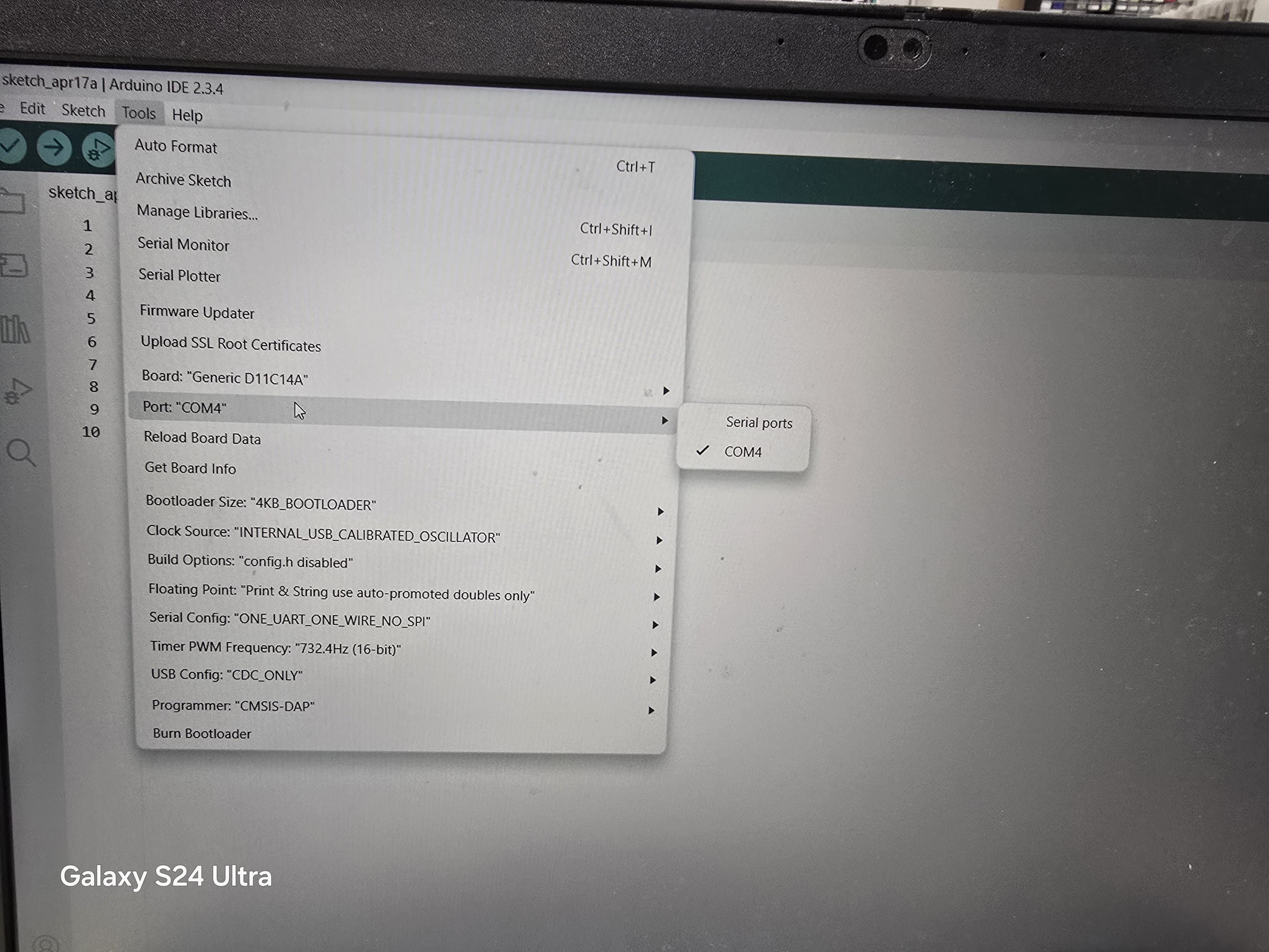
Then make sure its COM port is known - in this case the SWD programmer is COM 4
Now connecting the SWD Programmer to my development board with SAMD11c
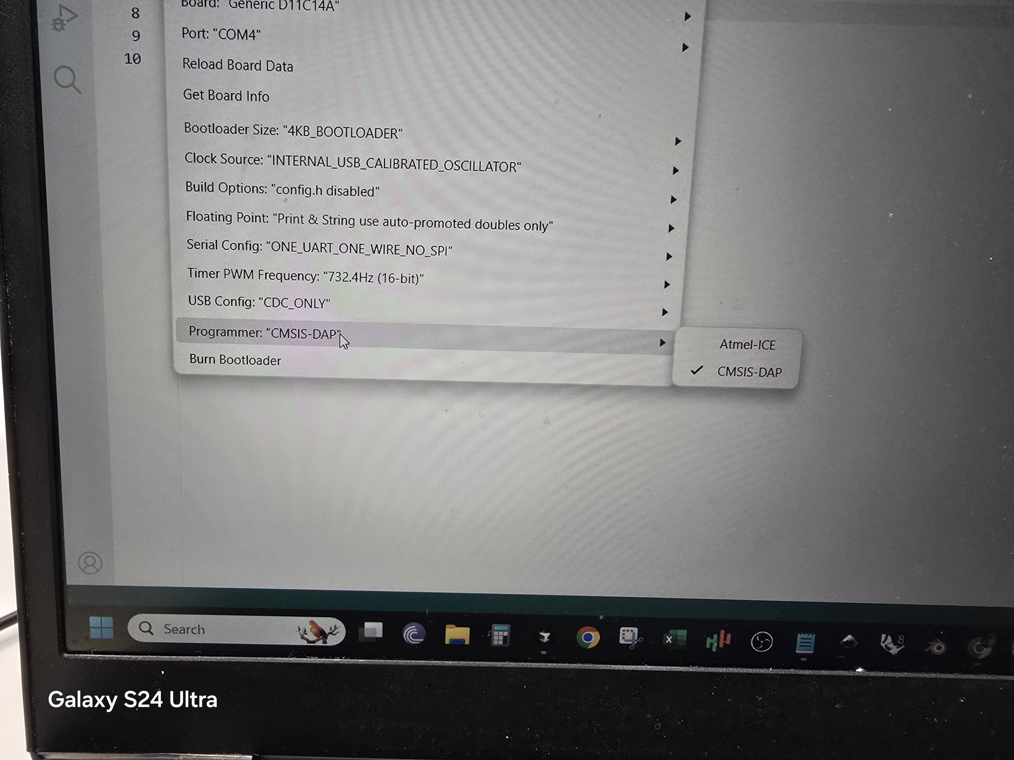
Now make sure that CMSIS-DAP is selected
Then we click on Burn Bootloader