Week 4
When you realize you're actually having fun loosing diopters

Table of Contents
This week's assignment is a bit less creative but I find it a bit more challenging because of the manual part, since I've never done something like this before and it's all really new for me. Let's see how it went, you'll find all the documentation and material as you go on, and the new content table right below!
Using Mods
Milling
Soldering
Updates
Objectives
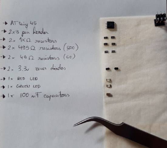
- Individual assignments: Make an in-circuit programmer by milling and stuffing the PCB, test it, then optionally try other PCB fabrication process.
Getting Started: Lessons and Machine setting
[18th of February]
We started the Week with a few introductory lessons with Simone, our Instructor, about what we will be going to do this week and best tips and practices for getting the job done. As usual I'll write some of my notes from italian as I go on, maybe these could turn out useful for someone as they have been for me.
We're going to work upon a base made from two parts, the most important of which is the copper one because the job will be created upon this side. It conducts electricity, the lower part does not, so it's important to keep this in mind in the process because it applies also to want you're going to dig and what you won't. For this week's assignment we're not going to create the PCBs ourselves but we're going to use some that were done by other students from previous years: I choose that of Brian, because I found his documentation to be really good for a beginner and exaustive. I downloaded the files that he has on his page, because for this work we're going to need two different things:
- one is the Traces file, with all the paths and the drawings;
- one is the Cut file, which is the external border of the PCB.
We have to be careful about some things, but these will probably be clearer in the weeks to come. For now, using the electronical design made by someone else is a good modus operandi to follow because it allows you to concentrate exclusively on the manual part: milling and soldering, which are the most important things of this week. That being said, Simone showed us how to use the Fab Mods in order to prepare everything for the machine to cut and engrave, both with a teorical lesson with the program and then with a practical lesson where he showed us the process of work and the steps to do. Let's follow them together.
Using Mods
[Started 19/02/2021]You start with Mods, which will help and guide you in the process of creating and preparing the files that you're going to give to the machine in order to mill your board. You have to insert your file (either the traces or the cut) using the Select png file button - and check the dimensions of your work, so that you don't find yourself that you file is bigger than your board. One important thing is the quality (dpi), which has to be around 1000 dpi - so remember to check that out.
Then you move to the next mod, and you have to select either mill traces or mill outline, based on what you're doing - you don't have to change or adjust the parameters that you find written there, so you can move on to the next part.
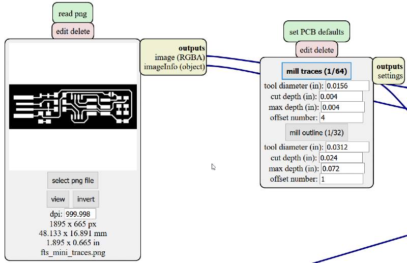
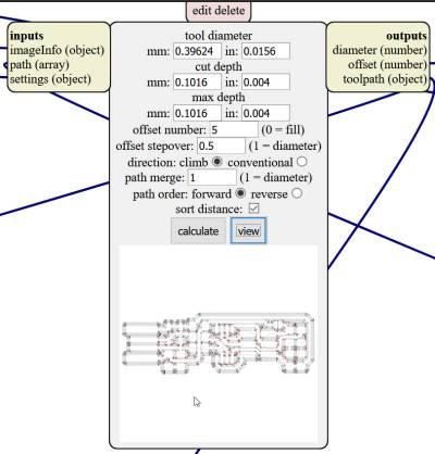
Then you move on to the next mod, where you can find useful information such as the tool diameter, the cut depth and so on. Here you might want to change the offset number, which I learned from using Fusion is the space that you have between the line that you want to cut and the cutting of the instrument itself. Usually for this week's assignment you don't have to change the offset number, but reading Brian's documentation I've seen that he advises to increase the number of the offset to 5 (because he had to remove manualy a copper part in the usb slot space). He thought that this might help to have a final base where you don't have to do this, but in the end as you will see going on I had to remove it manually anyway.
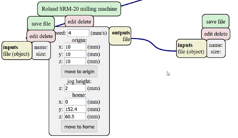
Now you're ready to go, you might start milling! Take your saved .rml files (traces and outline) and go to your machine to start milling them, assuring yourself to pay attention to all the measures to do a good work.
Milling
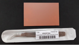
[From 19th of February]Then you can move on to the milling part, where you have to pay attention to a few very important things - since we nearly brake the machine because our drilling bit was not tight enough in the housing. First of all, we received our Kit! (*drums rolling*)
Then we moved to the machine, where you have to insert the drilling bit manually and pay attention not to drop it because it has a very fragile tip and you might break it entirely if you drop it on the sacrificial panel. You have to use two different tips, one for the traces and one for the outline, the latter is a bit larger and stronger since it only has to cut the whole board part to cut the part that you want from the pcb itself.
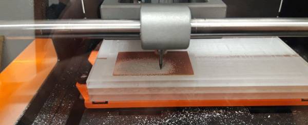
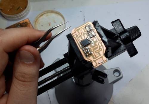
It's very important to clean well the panel before positioning your copper board on it, as it might move or slip away while you work and you ruin everything. Some of my collegues had their board completely move away, so I apply a lot of double tape underneath it - even a bit larger than the board itself as it might have a better grip upon the sacrificial layer. If you did everything correctly, the machine will cut everything until the end - you'll have to change the drilling bit when moving to the outline part and set again the X/Y, and your Z, so pay attention to it.
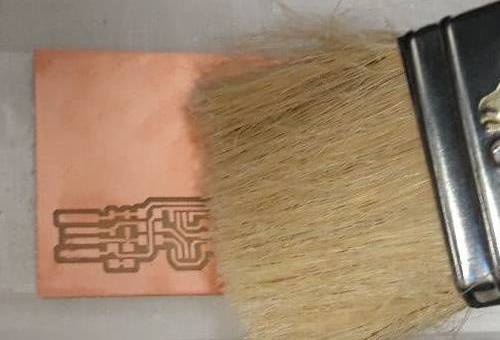
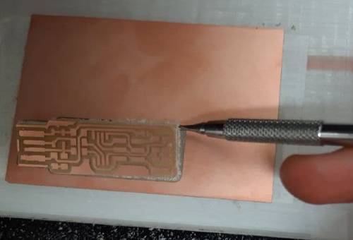
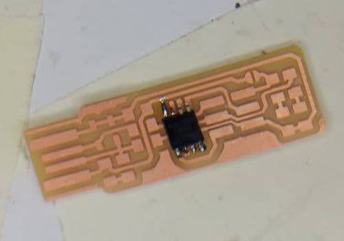
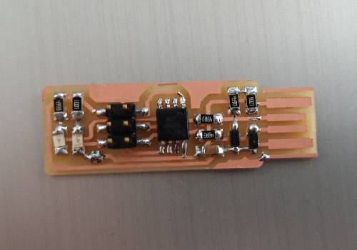
Remove the dust carefully, then you can remove the board (be gentle with it, with this kind of strong double tape you might actually risk to break it if you apply too much strenght). Remove all the double tape from the board and from your fresh and new pcb, then use some sandpaper to clean it and remove parts that might have sticked to it, and wash it with water and soap, drying it carefully so that you don't accidentaly remove copper parts that you need.
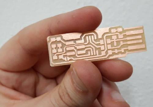
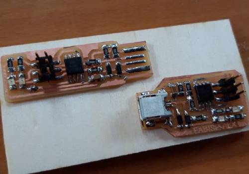
So there you have it! It's beautiful, I really shouldn't fall in love so easily, but I really can't wait to try to sold it on Monday! Let's see how many diopters I'll lose.
Soldering
[22th and 23th of February]In the Weekend, I tried to do an improvement on my Dice Tower and I'll try to cut it today, so be sure to check out Week 3 in the Updates section! As for today, I'll finally try to solder and see how this works, I'm really excited about trying this out. I starte by creating my Bill of Materials, trying to find all the components in the lab drawers and Simone gave us the ATtiny45 and the 2x3 Pin Head.
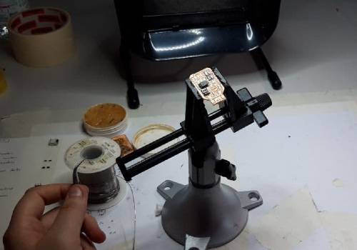
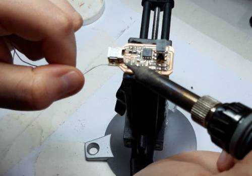
Having said that, I'm really stoned about how tiny this pieces are - I hope I don't lose them or break them because I'd probably not be remembered for my gentleness. So, since I tend to forget things quite easily if I don't write them down (and I didn't, when Simone was explaining how to solder), I started on my own and had some difficulties with it. When I tried to solder these tiny components most of the time they moved while I was working so I had quite a hard time to put them in the right position.
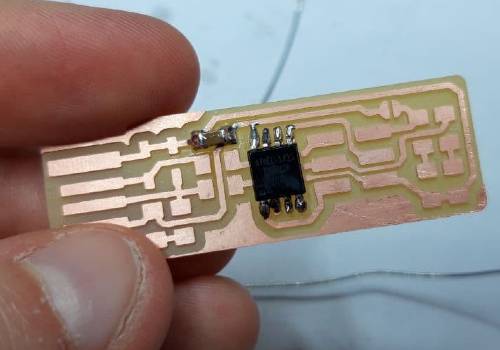
I made some mistakes, it's far from perfect. In some areas I had too much solder in others too few, and I really think I risked burning everything down from time to time. I realized that probably I didn't find myself with the position of soldering, trying to solder on the table hasn't really worked for me (probably because I'm quite blind). Once I started to use the support, fixing the board in it and having the lense and the light right in front of me I started to work better. After finishing, we worked on a terminal who already had the tool chain ready and we tested if the board was functioning - it worked, and when I tried to connect it to my computer everything was in order, so I'm really happy with my first attempt with soldering.
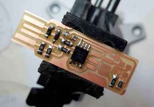
So, since we had some spare time, I decided to try to solder again using another design this time, that of Alex. This time I started applying the suggestions of our instructor, Simone, and tried to work better than the first time - and since it kinda relaxes me, I'm really happy about my two PCBs.
I'm probably starting to have fun with this, I think there is still a lot to learn on how to do the soldering better and surely I still have a lot of mistakes on my boards, but I think I made some improvements from this morning. In the meantime I'll start read some stuff about what are these components and how they work, there is still a lot to do!
Now I'll leave this for the documentation the screens of the code working and the tests of the PCB:
Updates
Programming the Programmer
[12th of March]
After a long introduction about how microcontrollers work and how to connect our PCBs, we started talking about how to make a computer talk to a PCB and how this one can talk to another PCB as well. This is a process that involves different kinds of tasks, but one of the most important of them is the telling our PCB that it has to become a Programmer: this PCB will later on be useful in order to program another one, which will become your Programee. This might sound confusing at first sight, so I do recommend you to read this part first and then, for further explanations and istructions, go to the Embedded programming week as well.
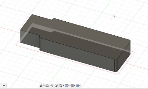
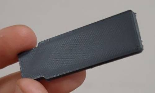
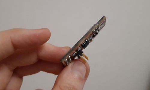
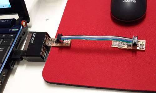
Since my PCB didn't had a good contact when inserted into the USB door, I had to create in Fusion 360 a base, which I had to glue to my PCB and give it a little bit of structure, a solid structure that will make it easier for me to connect it and for it to avoid breaking. While waiting the glue to have effect, I started working on the part that is necessary to program everything.
In order to do so, I followed Brian's Guide either because it's very clear and because he's the same one that made the PCB that I want to become a Programee. I had to follow some steps, that made me have some problems during the process because I was doing a mix between his documentation and one of a student from last year in our laboratory, and I didn't pay enough attention to were I saved all the files that I needed. I advise you to have care of these first steps, because if you do you'll never have too many problems. In order to program your PCB to be something or to do something, you have to install some things:
1) Download the AVR toolchain for either Windows/Linux/or whatever are you using the moment. You can do so by simply logging in on Microchip and downloading the version that you need, you'll get a .zip file - pay attention where you save it and where you'll decide to unzip it.
2) Download GNU make, remember here as well where you save and extract the files.
3) Download AVRdude, this will help you do all the things that you need to tell your AVR what to do.
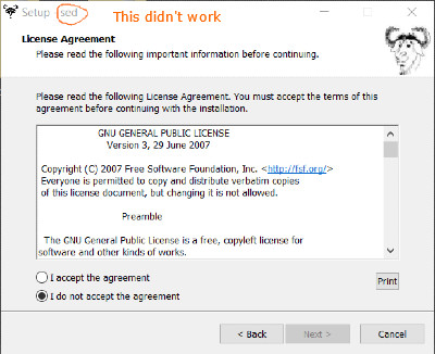
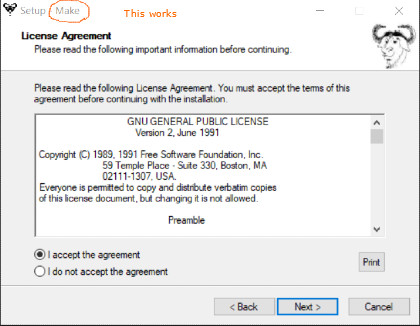
Some problems that I encountered had to do with the "Gnu Make" file, because it always downloaded me a "sed" file and when I wanted things to work they didn't. I checked most of the things twice or trice, without knowing what was going on, and then I had to disinstall and cancel some folders and try to download the GnuMake file again paying attention to what it said during installation. They have the same icon and installation, but the second one has a Make file that we couldn't find in the first one, so if something goes wrong be sure to check this out, it might help.
4) After downloading all of this, you have to change your Paths in your Computer. We do this because we want to tell Windows where to locate all the files and tools that you installed, in particular when you type them in the command line. To do so you have to go to Start Menu -> Control Panel -> then head on to System: from the left side you have to choose Advanced System Settings and click on the Environment Variables button. My screen is in Italian, so please do forgive me, but on Brian's documentation you will find it in english - if it might help, here's a screenshot of the Three Paths that you'll have to create.
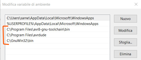
Be sure to have the right path selected, if your folder are saved in different locations in your computer you obviously have to select that path and not mine. Use the "Browse" option to help you find the folder that you need, I decided to go for the same folders that Brian used because I wanted to avoid problems.
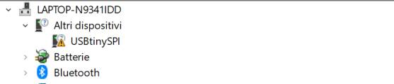
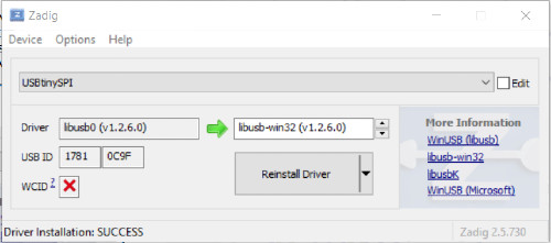
5) Then you have to downloadZadig in order to get the Windows Drivers that you need in order to program your programmer. Plug you programmer PCB to you computer and open the window of Zadig, you'll have to go on Options and be sure to select "List all Devices, so that you can see your AVR: mine is "USBtinySPI". Install Driver and you're done!
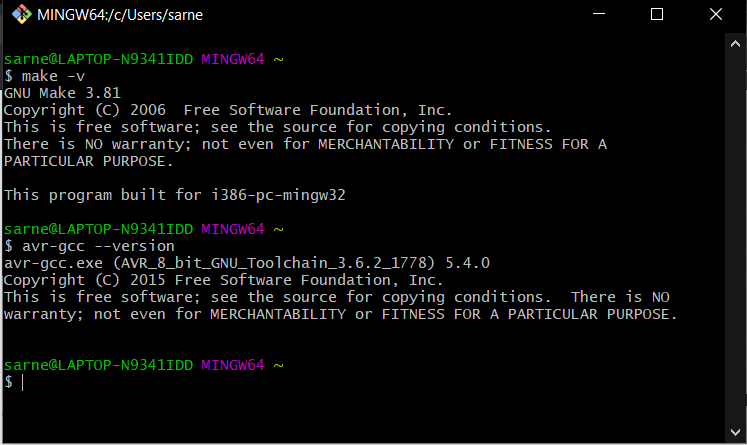
6) Now you'll have to check that everything is in order by opening Git Bash and give it a series of comands, let's see them step by step:
- Make
Type make -v and press enter, and if you find errors it means you made something wrong in the installation of make (as I said up, with the setup) or made some mistakes in your paths.
- avr-gcc
Type avr-gcc --version and you'll find some strings of code, here if you find errors it's due to the installation of the Atmel toolchain or path settings.
I had a Problem during this process because I switched from different documentations and they used different microcontrollers (one was ATtiny44 and the other one was ATtiny45) so some strings of code didn't match. Be sure to check that you download, install and follow things that you need for that specific microcontroller that you use, as I said before I do this for the ATtiny45.
- avrdude
Then you connect your USB port and type avrdude -c usbtiny -p t45 and press enter; here if you find errors it may be because you have problems with the USB driver installation in Zadig.
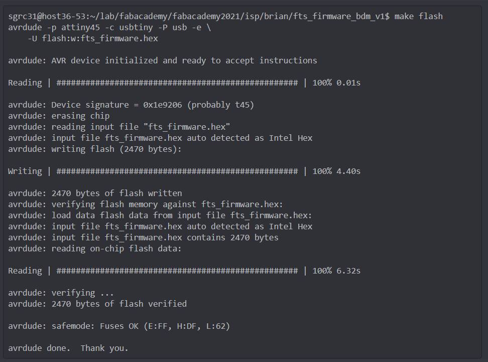
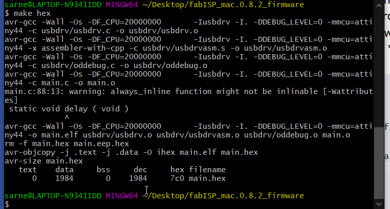
7) Download the firmware source code and unzip it, going into the terminal and going with cd inside the directory. Once inside, type make and it will create a file for ATtiny45 which will be called fts_firmware.hex. Hex is the file that "speaks" the language of the chip, you'll need it soon after.
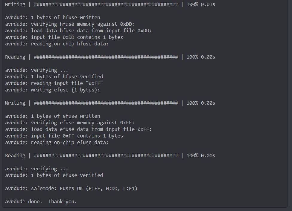
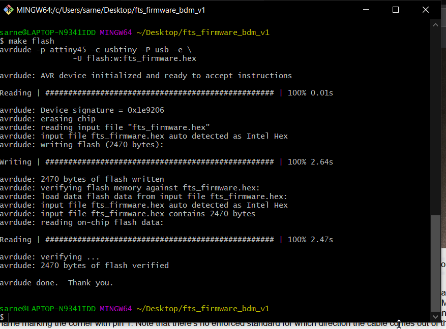
8) If everything is in order, you then move to the last things to consider. Keeping the programmer connected with the computer you run make flash, which I learned will erase the chip and program it with the contents of the .hex file you made before.
I suggest you, as usual, to check also Brians documentation for more detail, he really did an excellent work and I'm only trying to do a clear explanation myself but I might miss a lot of detail along the way. This processes worked for me, in the end, so I hope they will for you too.
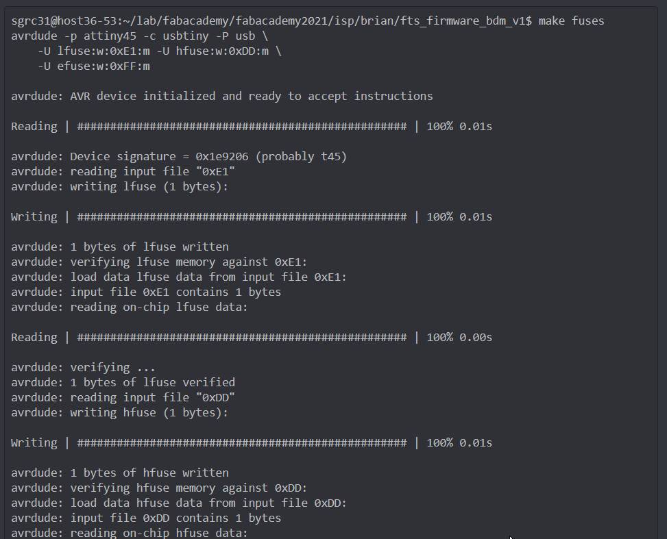
9) You then use make fuses command, which will set up all the fuses except the one which disables the reset pin. For this one you'll have to run make rstdisbl, and at this point you're finished! You can move on. Well done!