Electronics Design
week 6 Group assignment is to explore and use the test equipment in our lab to observe the operation of a Microcontroller circuit board
Basics of Electronics
Before we begins this week a small basic electronics class were taken by one of our instructor Yadu Sharon. That was not necessary for me because I'm already know the basics from my Engineering Diploma. I'm the only one in the lab who has Electronics Engineering background. Any way its better to revise everything to start new design. There are a lot going in electronics to understand Yadu delivered some basics which required for this week assignment
Todays Electronics Industry is pretty big and its growing in each seconds. Because of that, It is more complex to define electronics in one statement. It's all about playing with motions of electrons to make control signals, clock signals etc...
Basic Components
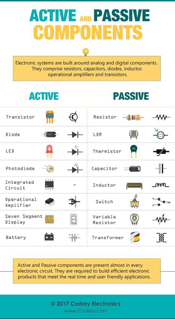
From the basics the components are distinguished by names of active components and passive components, The above table shows the distinguished examples of the basic components. This is done by their performance and use case in a electronics circuitry. And there are thousands of verities of electronics components available according to the use cases. We are only gonna focus what need to our own microcontroller board for this week assignment.
Resisters:-
It is one of the very basic electronics component used to control current or voltage in a electronic circuit. There are various types of resisters available. Each uses different applications. its measured as ohm and the values of each resistors will written on it with color codes. In SMD types it will written with number codes. normally we use in ohm ,kilo ohm (K),Mega ohm range resisters.
The above figure shows the picture and the symbolic representations of a resister. The figure actually shows a THT (Through hole technology) component resister type. The voltage,current,resistance law (v=IxR) is very impotent while selecting resisters in electronics circuit design.
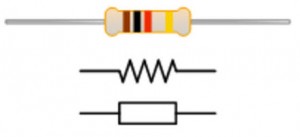
capacitors:-
Capacitors are one of the passive components group which mostly used for storing energy ,power supply filtration,high frequency coupling applications and etc... It's measured in Farad and normal use ranges are Pico Farad(pF), Nano Farad (nF), Micro Farad (μF or uF) ranges.
The figure shows the symbolic representations and pictures of a capacitor. The colors and shapes, labeling will change according tho the manufactures.
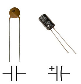
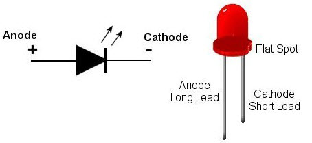
Diodes:-
A Diode is a semiconductor device which used for converting AC to DC (rectification) and Voltage Regulating applications in electronics.It's made on a small semiconductor element's wafer by adding impurities in a P-type N-type(PN junction) Combination.if we connect a diode in a circuit it only conduct in one direction and If we change the polarity of the diode or the power it will conduct the opposite but also will not conduct in the other direction.Normal Diode's Symbols and picture (THT) are given below.
Depends up on the applications there are various types of diodes are being used in electronics, like the diode which regulate voltages is called Zener diode.It will conduct in backward if the voltage limit reaches over the zener diodes value.
LEDs:-
The expansion of 'LED' explains the working of the Device which is Light Emitting Diode, So there are semiconductor Diodes used in electronics Which emit lights. And it's very popular we can find almost every devices and everybody knows about them.
LED is normally design with desired working voltage and current ratings.It also vary depends the Colour ,types and manufactures technology. the above figure show the symbol and an example picture of an LED.
Transistors
Transistors are the one of the greatest invention in the 20th century which revolutionize to the Modern electronics Industry. It's a semiconductor device Used to switch or amplify electrical signals and Power.It's the one of the basic Building block in electronics circuits which is categorized as active components type.
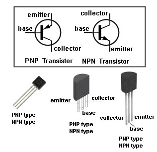
In the figure shows symbols and pin outs of transistors. basically there is two type of transistor available one is NPN and another one is PNP. Those three terminals are represents Base (B), Emitter (E),Collector (C). Base voltage controls the voltage-current flow across the Collector-Emitter terminals.
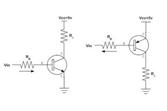
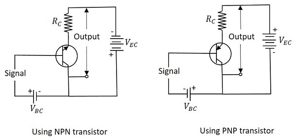
In this picture shows how an NPN and PNP transistors used like a switch triggered by the base voltage in a electronics circuits.The picture below shows how it connects as signal amplifiers.
The bipolar transistors are older technologies now, because of their heat conceptions and Impedance problems . SO todays we use MOSFETs aka Metal Oxide Felid Effect Transistors.
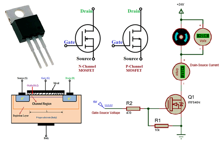
The Isolated Gate technology allows High Impedance because of that it has High frequency switching capabilities and only consumes low energy than a Bipolar transistor.
Integrated Circuits (ICs)
The idea behind the Integrated circuits is just like the name to Integrates millions and billions of the active components inside a small pice of a silicon.So this kind of silicon chips made our digital world revolution faster to our finger tips and still growing by the mores low which says the capacity of integration process will be double in every year
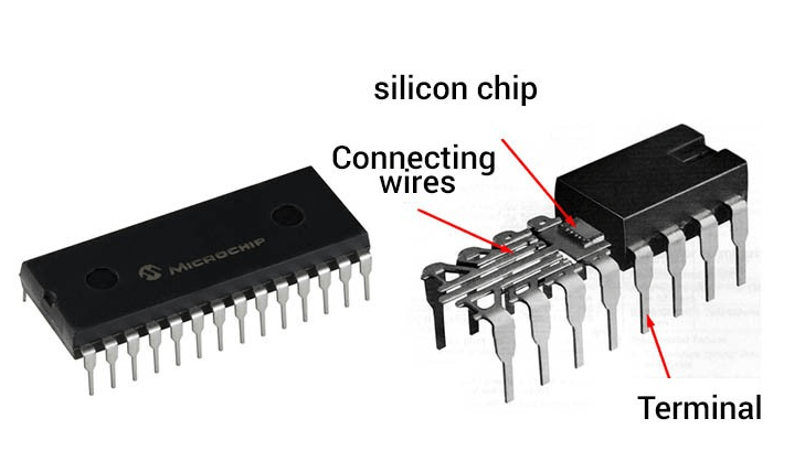
The above picture shows the how the silicon chips are look like in side the plastic package that covered around it.
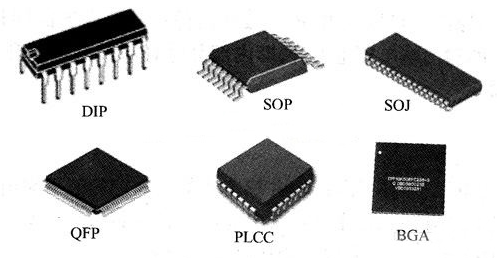
Here is the different package size of iC available in market which uses according to the applications.
Switches
Switches are very basic Input component in Electrical Engineering so There are tiny varieties of switches used in electronics . It's available depends on the applications we used.
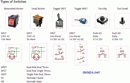
The very simple switch we used is tactile push to ON switch for instant inputs like in our keyboards and mouses. Also uses the slide type switches for turn on and off functions.
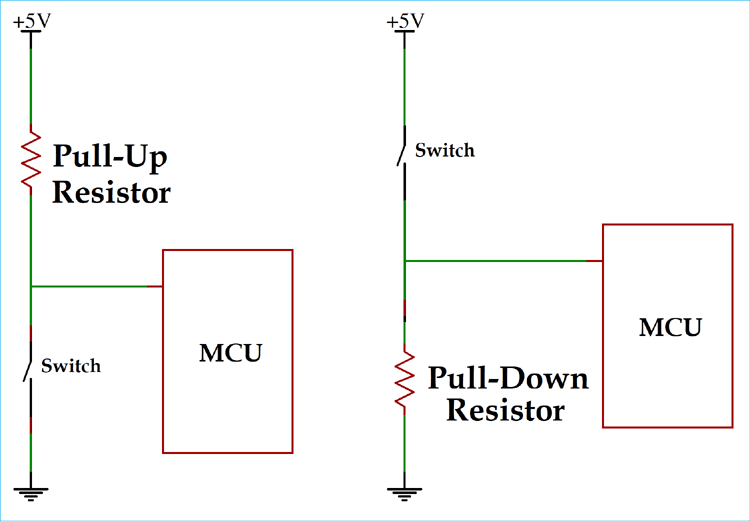
Here is how a simple push button connected to a microcontroller as Input device . The both methods are uses a resister called Pull-up or Pull-down for removing the noise at the microcontrollers input pin. If we didn't use any resistor like these those will affect the input like a floating action between GND and VCC which result unpredictable input if the switch is not active.
Test Equipments
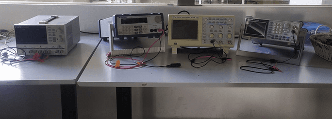
In electronics, Processes like testing ,Troubleshooting and analyzing uses various types of Test Equipments In the LAB.That include Lab Bench power supplies,oscilloscopes,Function generators,multimeter... etc.....
Digital Multi-Meter
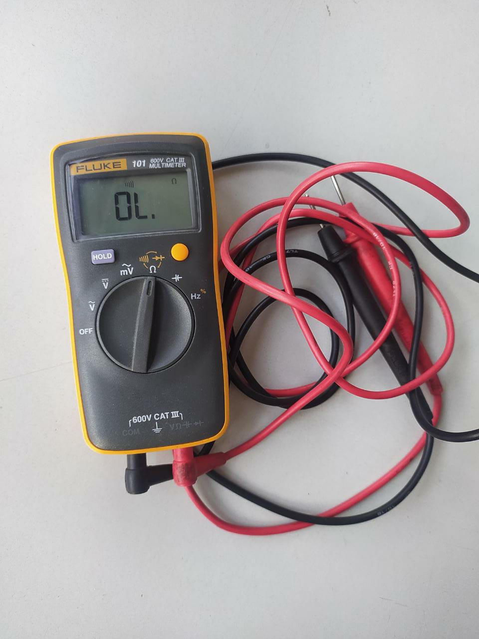
Multi-Meters Are first prior handy test equipment uses while working with electronics. It can do several measurements like voltage(both AC and DC),Current or Amps(some supports Current) ,Resistance,Capacitance frequency etc... mostly uses for troubleshooting purposes because it has a continuity(short) check option and some even support transistor testing
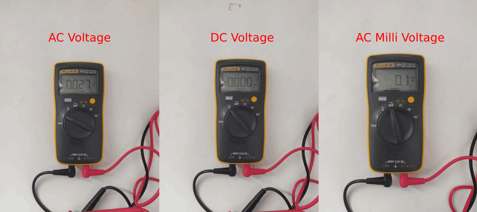
From the Fluke 101 Multimeter we can measure AC Voltages, DC voltages and AC voltages in Millivolts range All option has Auto ranging Features.
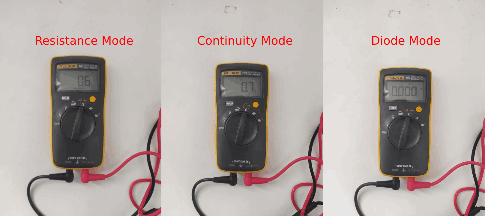
And of course also have resistance mode with Auto ranging. Auto ranging Feature is awesome, It automatically detect the the Measuring scale range and shows in the LCD. And in the same selection we have continuity buzzer tester and a Diode Mode we can chose them using the Yellow button on right top under the display.
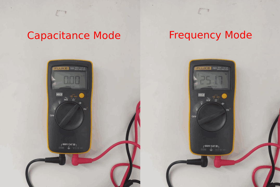
These are special modes for Measuring Capacitance and frequency directly.It will be more helpful when we works on unlabelled SMD Capacitors. Only some special Multimeter has these features and Some of them Capable to measure Current (as a Ammeter) in a circuit.Another Advantage of this Fluke 101 model Multimeter is ,It works only 2 1.5V AAA type battery which is easy and cheap to replace and also not harm full while checking 3.3 v logic leveled circuits or components.
DC Lab Bench Power supply
This is another Important Equipment which used for power up the circuit boards or electronics devices while testing.Lab bench Power supply alow us to vary ( with a knob or digitally ) the current and voltage for setting the output voltage.
In our LAB we have two types of bench power supplies. one is dual-channel Digital and varying out put voltage 0-30v/0-3A another one is single channel (0-30v/0-5A) digitally programable one.
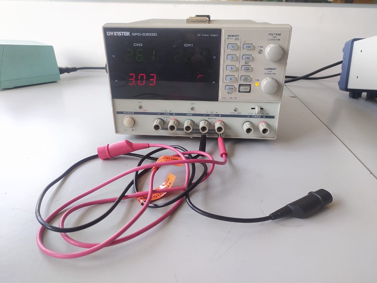
The above one is Dual channel Digital power supply from GW-INSTEK. Which has 2 varying (0-30v/0-3A) and one fixed voltage (2.5v,3.3v,5v/3A) outputs. We can adjust voltages and current using the knobs and also possible to turn on and off the outputs and channel selections using the buttons. For more check out this link from element14.
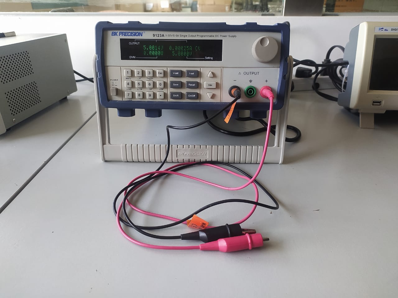
This one is a single channel 0-30v/0-5A Programable power supply. One of the feature I like on this one we can set const voltage(CV) or constant current (CC) for the output just using the keypads.And it is also expensive compare to the other one
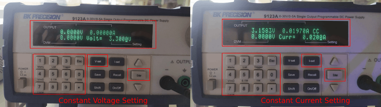
To setup the constant voltage or constant current, we can enter the values of voltage or current by using 'V-set' ,'I-set' buttons. At the power on the voltage will be 0.00v and the output will be off. For constant voltage after setting up the voltage the current will load default upto 5A. Or we setup the current after voltage that will be a a constant current setting. It will show the (Constant Voltage) 'CV' or 'CC' (Constant Current) on the display while turning on the output.
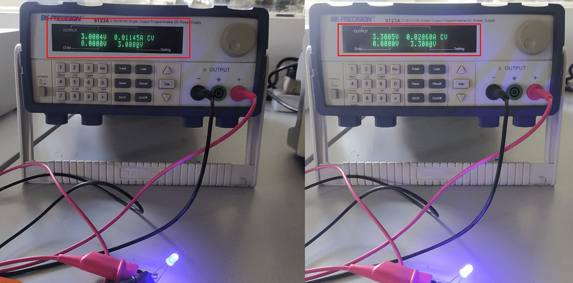
We connected a blue LED in Constant voltage method to try out the bench power supply. It bright up at 3 Volt with 0.01145 Amps (11 mA) and at 3.3 Volt with 0.0286 Amps (28 mA). The current is provided upto 5Amps, the led only required around 20-30mA to light up.But,if we increase the voltage that will allow to pass more than 30mA current through the LED and it will burn up.
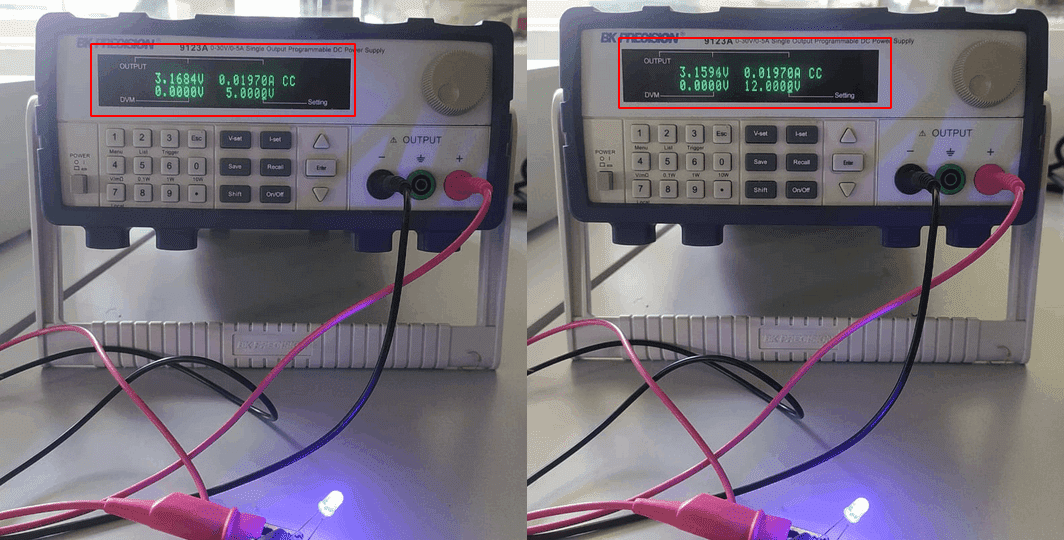
In Constant current setup we setup a 20mA (0.020Amps) Constant current with different voltage level which is 5V and 12V. So here no matter how much the voltage is it only use around 3.16 Volts for it's working at 20mA that gives us Power of the lED (Watt) = Voltage x Amps ==> 3.16x0.02A 0.0632 watt or 63 Milliwatt.
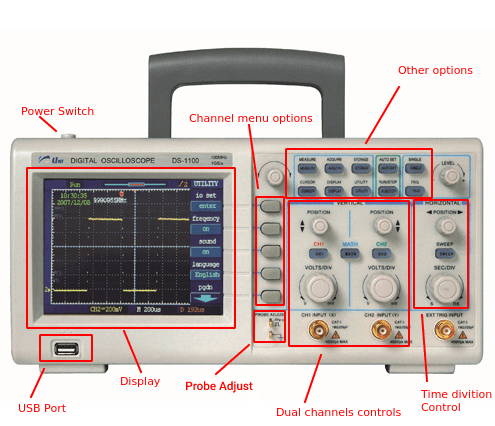
Digital oscilloscope
Oscilloscopes are more Important equipment while designing electronics circuits which related to signal processing.It's a great analyzing equipment in a electronics LAB. There are two types oscilloscopes used in Industry. one is old CRT tube based CRO - Cathode ray Oscilloscope and another one is Digital Storage Oscilloscope or DSO.
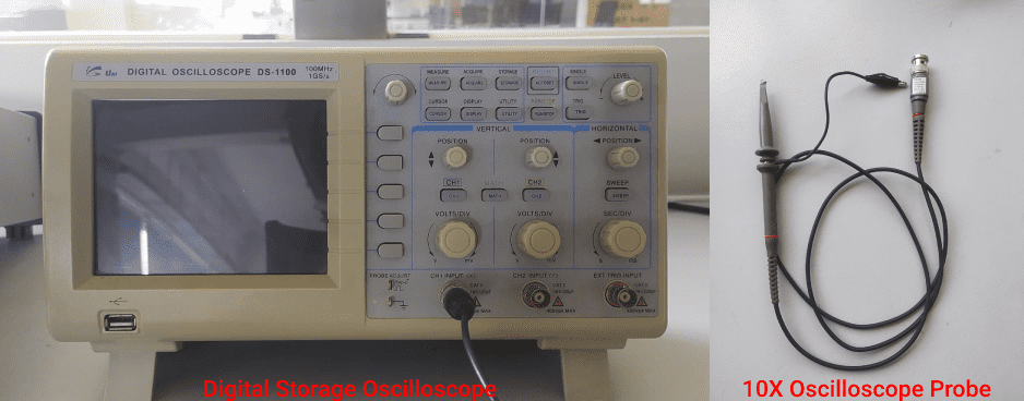
Our LAB has a Digital Storage Oscilloscope(DSO) because it has more function,less space utilize and new technology. This one can capture signals upto 100 Mhz and comes with dual input channel and external trigger input. most importantly its a storage scope we can capture and measure the signals and also can download the signals into a USB Storage device
This Oscilloscope from a company called UniSource we can find the data sheet here. In order to use the DSO which required a probe that comes with it. The probe is labeled X1 / X10 with a switch for selecting.
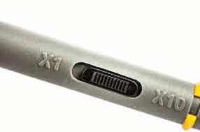
We can see the selection switch on tope of a standard DSO probe. where X10 is the recommended option for common use cases X10 option supports an internal circuitry inside the probe. X10 only allows one 10 th of the signal to pass and also support higher frequency signals to the scope.This is called attenuation. Switching X1 is avoid the internal circuitry allows users to connect directly to the scope. X1 is suitable for low amplitude or low frequency use cases. Its important to change the settings in the scope channel's menu for the X10 or X1 selections
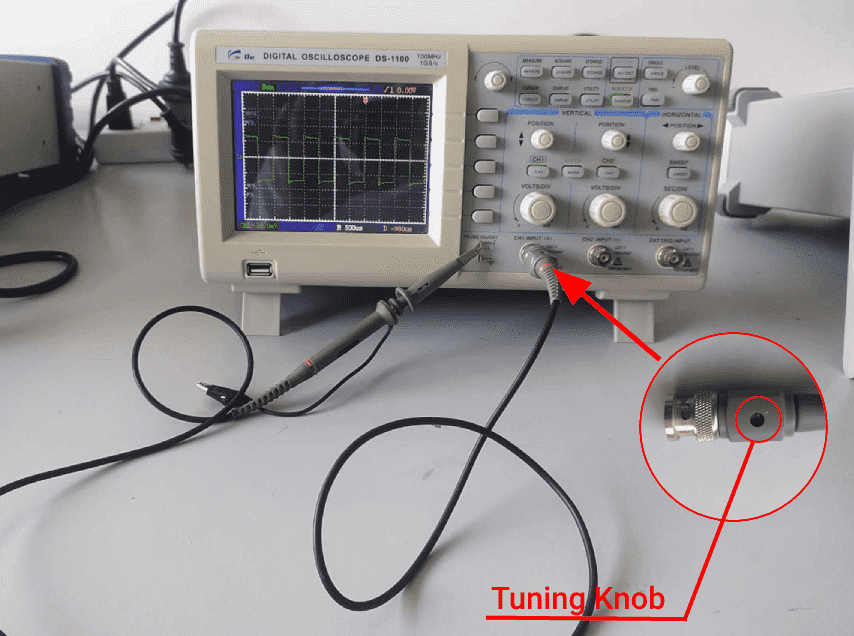
After connecting the probe we can hook up to the sample 'Probe adjust' signal out (square wave pulses) on the scope for testing the results. If the showing square wave's edges isn't correct we can adjust that by tuning a small trim capacitor knob or tuning knob on the CNBC connecter of the Probe with a help of a small screw driver.
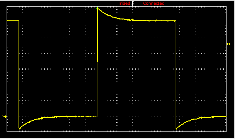
The results of tuning the trim capacitor knob on the probe look like the above gif Image. fore more check out this Tutorial from gpslimited.com
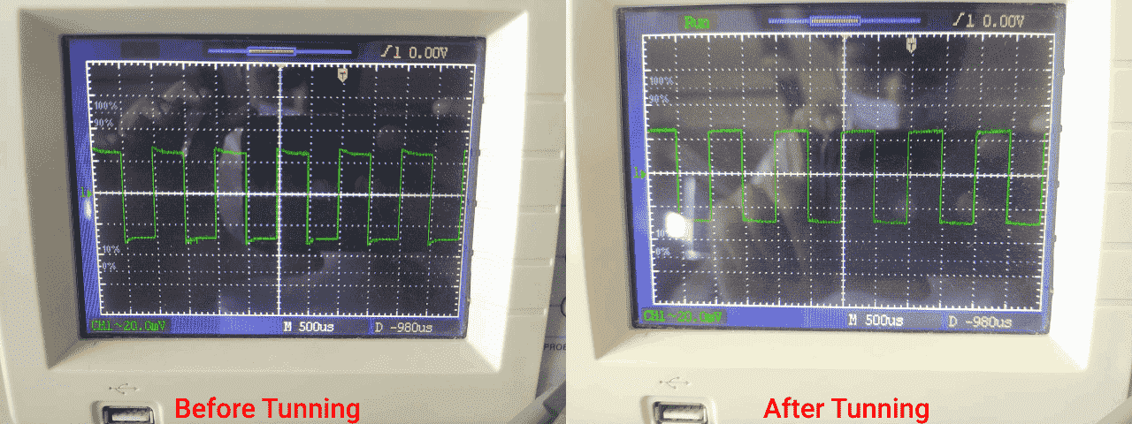
The above picture show the square wave pulse before tuning and after tuning
Function Generator
For testing or simulating circuits or devices like amplifiers,speakers, signal processing circuits..etc.. is done with the help of a Device called Function generator. it generate various types signal waves lke sine waves,square waves,triangular waves,noise etc.. with variable parameters ( frequency , amplitude,duty cycle).
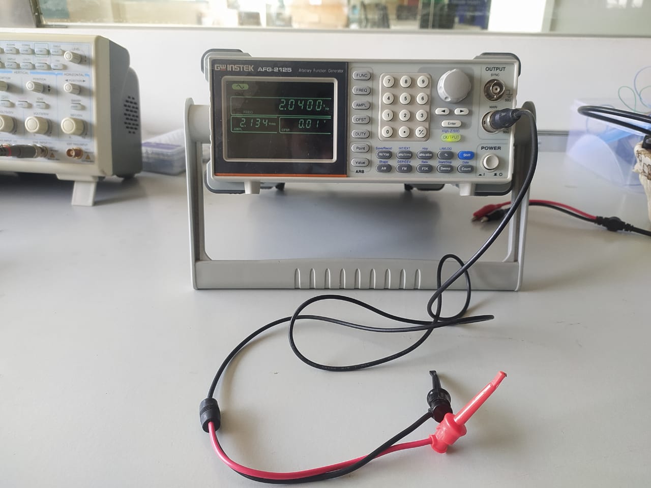
In our lab we have a AFG-2125 model Arbitrary Function Generator from GW-Instek. For the learning purpose as a demo we connected a speaker in the output of the function generator and tested out the waves through the speaker with varying frequency.
The above video show the out put sound coming out from the speaker with different wave shapes @ 1KHz and with a 5v Pk-pk amplitude.
Here is, in the video show the speaker output hearing test on a sine wave signal which vary 20Hz-20KHz. we can only hear signals from 15Hz-15Khz properly.
Testing and Observing a Microcontroller board
For microcontroller testing with equipments we used an Arduino Uno. Because its the one most popular microcontroller development board in the world also in our lab. And its based on 8 bit ATmega328 microcontroller from Atmel
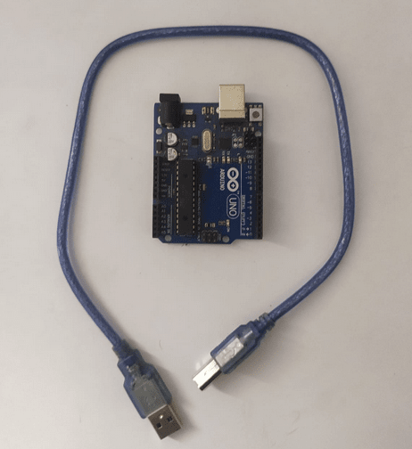
Here is the picture of an arduino UNO development board and a USB B type cable for connecting to the computer. The development board is build with all the components required for the working of the Atmega328P microcontroller
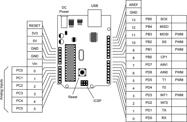
The above diagram shows the pin outs of the ATmega328 Microcontroller in the Arduino UNO R3 board. It has 14 digital functioning and 6 analogue functioning pin outs. Most of the kids who interested in electronics and programing know this Board and also know to use them.
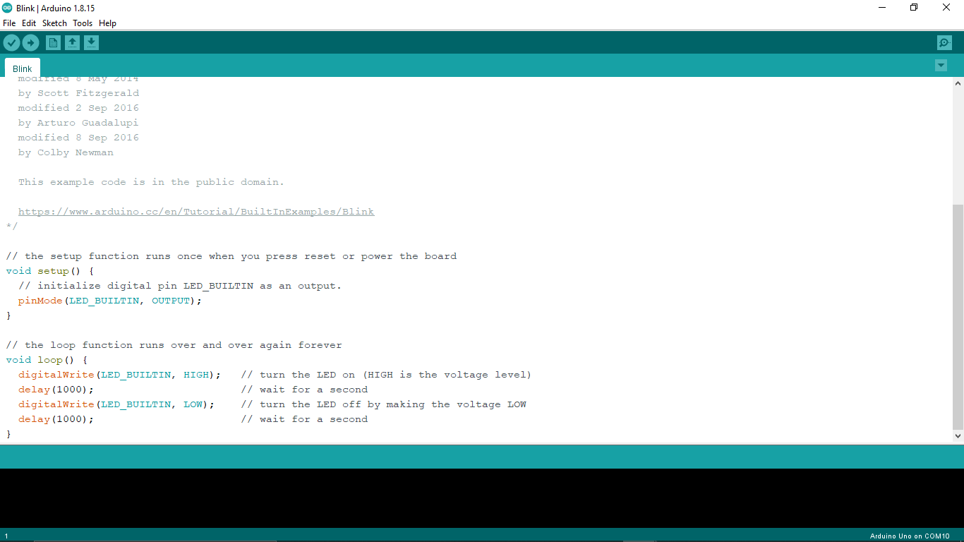
Using the arduino IDE we load a basic LED blink program with the help of instructor. This allows an lED connected to the digital pin 13 of the arduino 'ON' and 'OFF' periodically with 1 second time delay. Find more about the software and Arduino from the arduino.cc official website.
We connected the programed arduino UNO board to the DSO and also gave 5v power from the lab bench power supply. From the observation we got a square wave output on the DSO's LCD screen which is turn up and down periodically with respect to the LED blinking in 1 sec. And the frequency measured by the scope is 0.5Hz with 2.0 second time period which mean one HIGH and LOW takes 2 second to complete.
On the Power supply showing that the arduino takes 0.0437 Amps which is around 44 mA on the LED turn off period and that's the Arduino UNO's or Atmega328 microcontroller's ideal current consumption.when LED on state it going up to 94mA .It is 50mA higher than the off state because that's the both LED's total power consumption. (Apart from external LED there is an ON board LED in the Arduino UNO board)
Then we re programed the arduino UNO with another ARDUINO examples called Servo Sweep program. This program used to control a servo from 0 degree to 180 degree and vise versa using a PWM (Pulse width Modulation) Signal from the microcontroller. we can see the signal duty cycle (the time taken of staying on HIGH or LOW state) changing according to the servo's angle change.
Electronics CAD
Easy EDA
EasyEDA is a could based web application by Chinese company.using a cloud software has many benefits.we can log in from any PC only need a browser and internet connection . I use this CAD application a lot I love the app.we can create gerber (PCB CAM Files) files and also get Monochrome PNG,PDF documents. EAgle ,Kicad ,Altium Libraries are supported
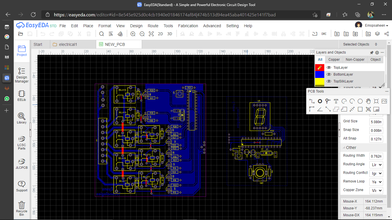
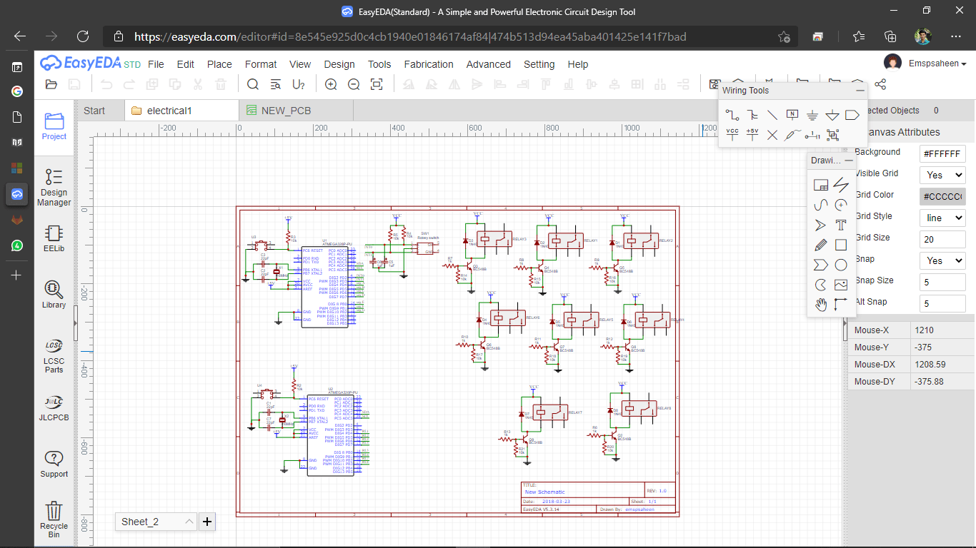
Easy EDA PCB Environment
Eagle CAD
Eagle cad is one of the popular Electronics Design tool acquired by Autodesk.During FAB_xL program by FAB LAB Kerala in 2016 Eagle was introduced to me
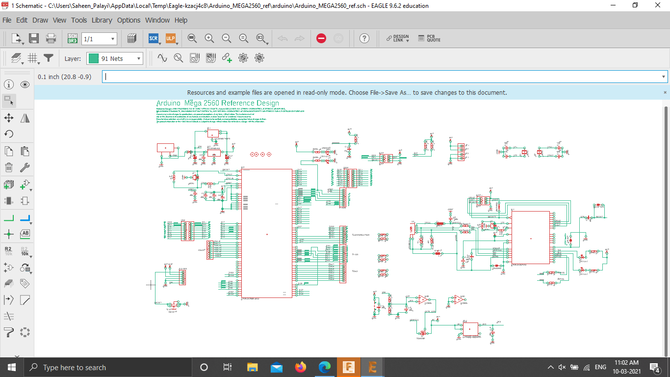
Eagle's Schematic Environment
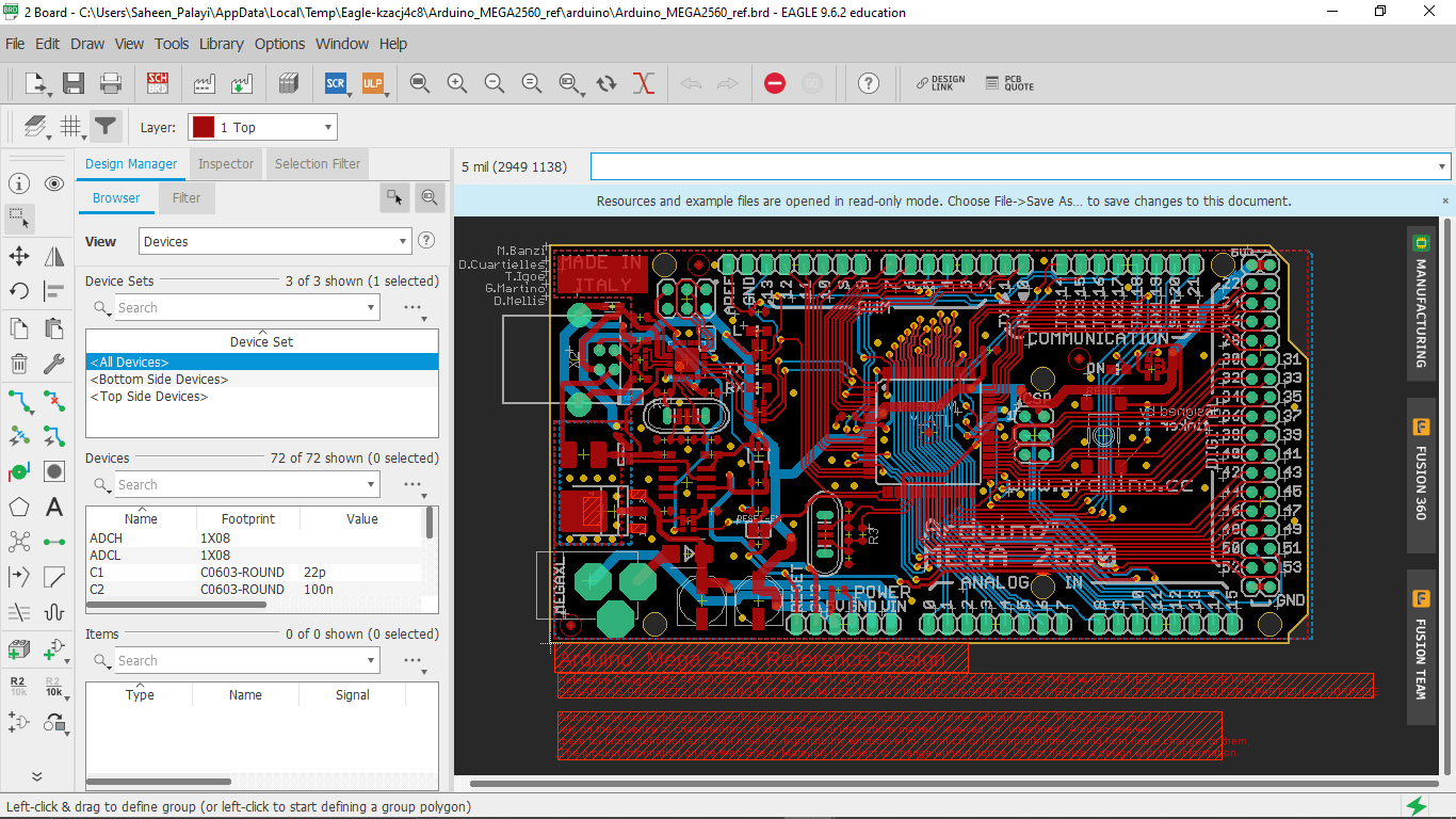
This is Eagle's PCB Environment
week 6 assignment is to redraw an echo hello-world board, add (at least) a button and LED (with current-limiting resistor) check the design rules, make it, and test it extra credit: simulate its operation
Sketching the Echo Board
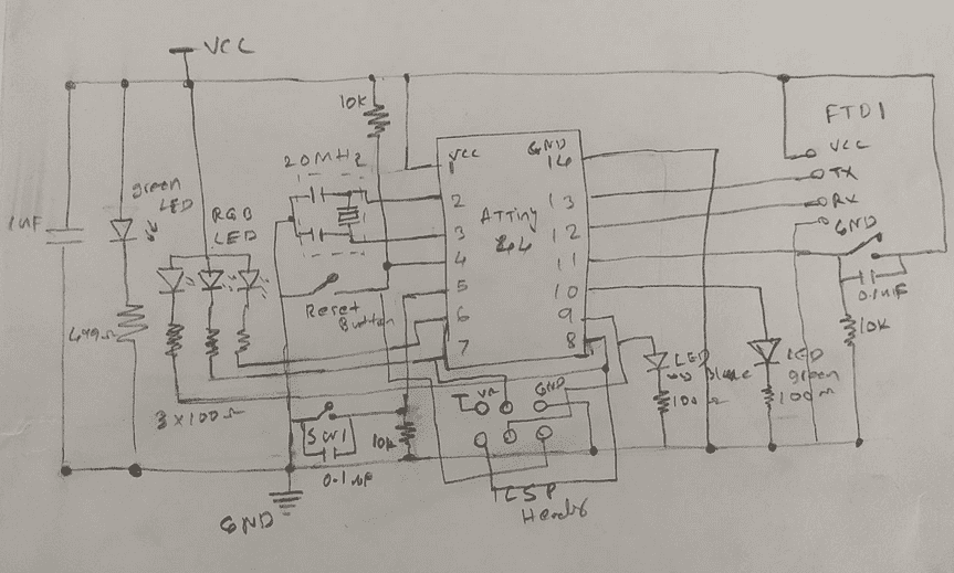
For redrawing the Ech hello-world board a basic model is given with minimum components to done the job.I have to add at least a Button and an LED to the redrawing circuit This week assignment is designed for those guys who doesn't have any experience with electronics.But,I already know all about the assignment then I redraws the circuit from neil's echo-hello world board and I planned to add two input button and 2 single LEDs,1 RGB LEDs.also added a power led and a button for resetting board
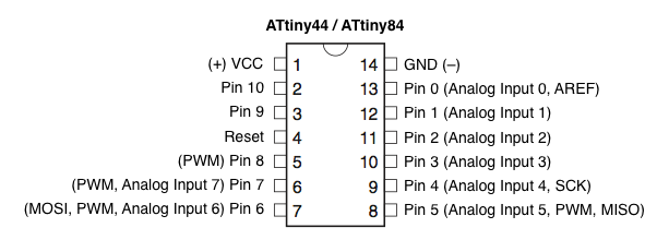
Also refers the pin diagram provide from the Attiny44 data sheet
The thing is you have to know what gonna design and whats the function of each component, but this assignment is like a test experiment on Electronics CAD design.
PCB in Fusion 360
After the redrawing on a paper I chose fusion 360 for designing PCB .The new feature of fusion 360 alow to draw E-CAD PCB models in it also 3D PCB models.I always use EasyEDA also know some eagle CAD,Decided to try fusions anyway because I like fusion very much.The interfaces are much better than Eagle but all tools similar to Eagle .
I opened the E-CAD in Fusion 360 .Instructor shows me this,Autodesk includes the E-CAD in the fusion,I know Eagle and Fusion can be synchronize to work with 3D PCB Model for prototyping.this was awesome
by clicking on new Schematic opened an empty environment for drawing circuit diagram.It's mandatory to do the schematic before doing the pcb.
then I minimized all the side window for getting more space for drawing.
So the Fab LABS supports only some SMD Package components,so there are many components available by defaults also possible to add more from internet.So the FAB Suggests to design circuits by using the FAB_E-CAD_Library which provides on the FAB tutorial Page,See the Eagle Resources.
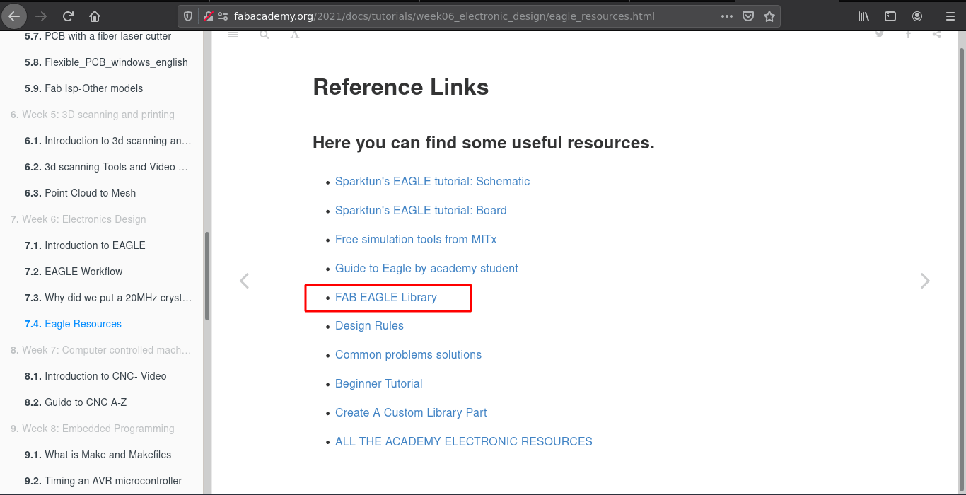
I downloaded the FAB Eagle Library from Tutorial page and Decompressed in my PC.
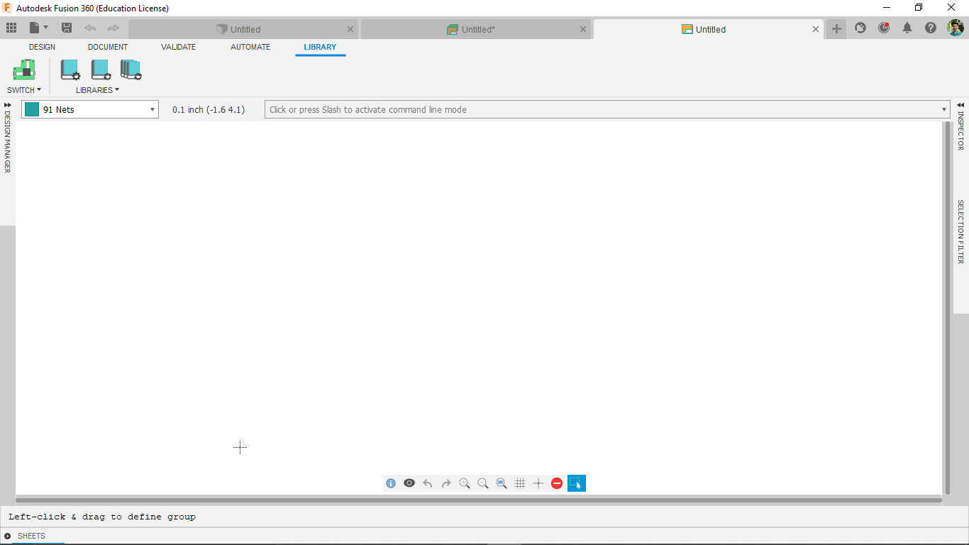
then I opened library manager in Fusion's E-CAD environment
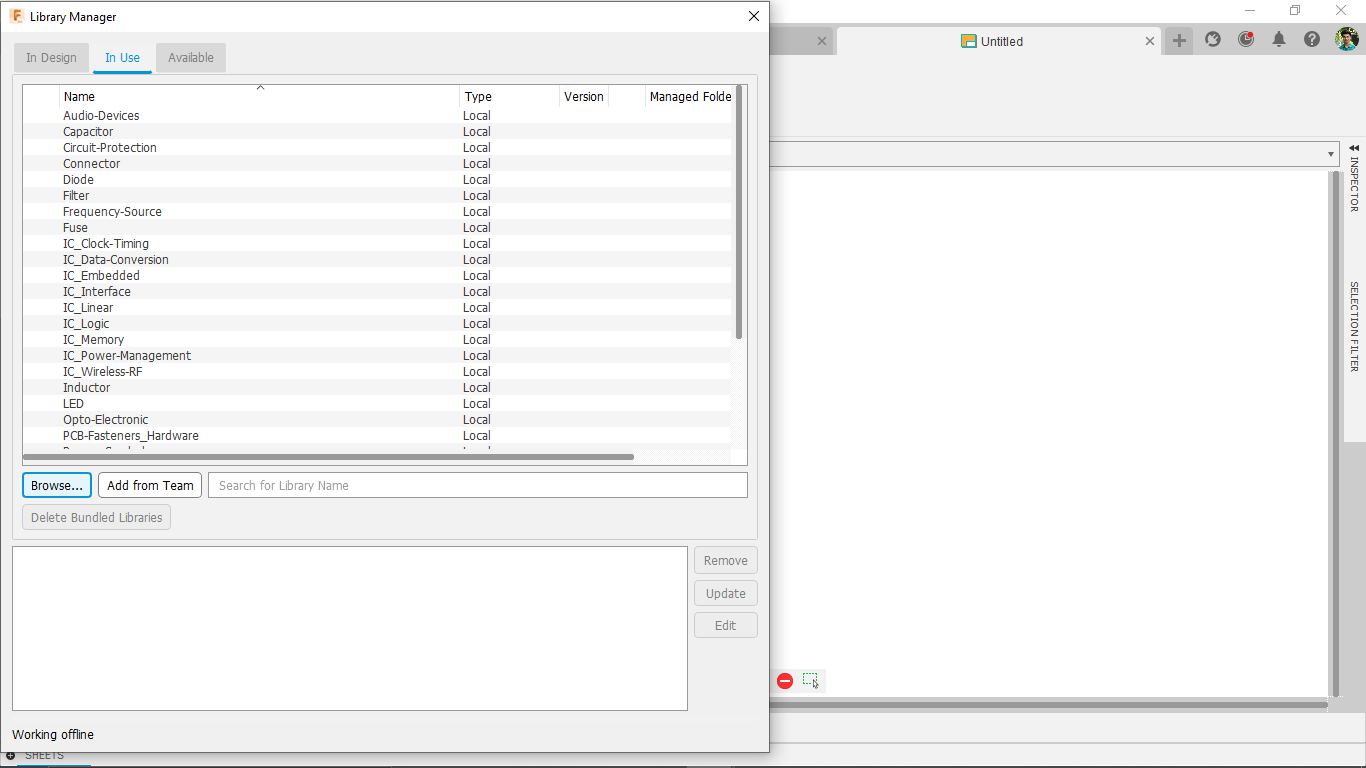
in the window browsed in my PC's files to add the Fab library to the fusion E-CAD
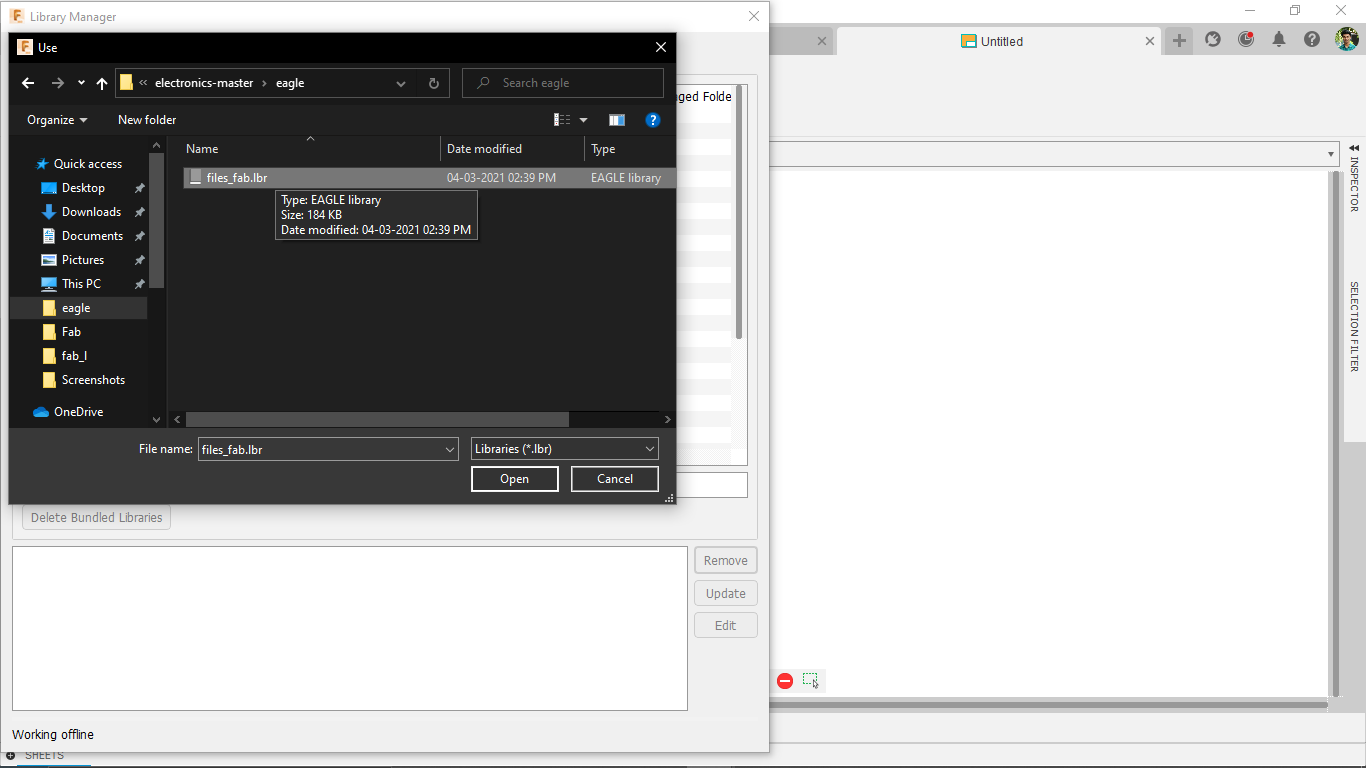
opened the library file to the library manager then I Update the library to the Fusion E-CAD
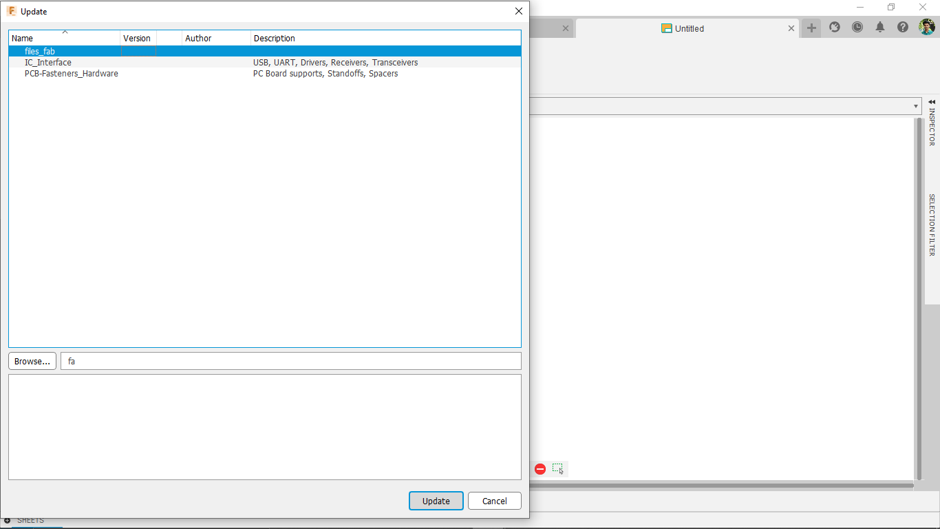
successfully added the FAB Eagle Library to the fusion PCB Design cad,Now I can add Components from FAB Library That fablab provides
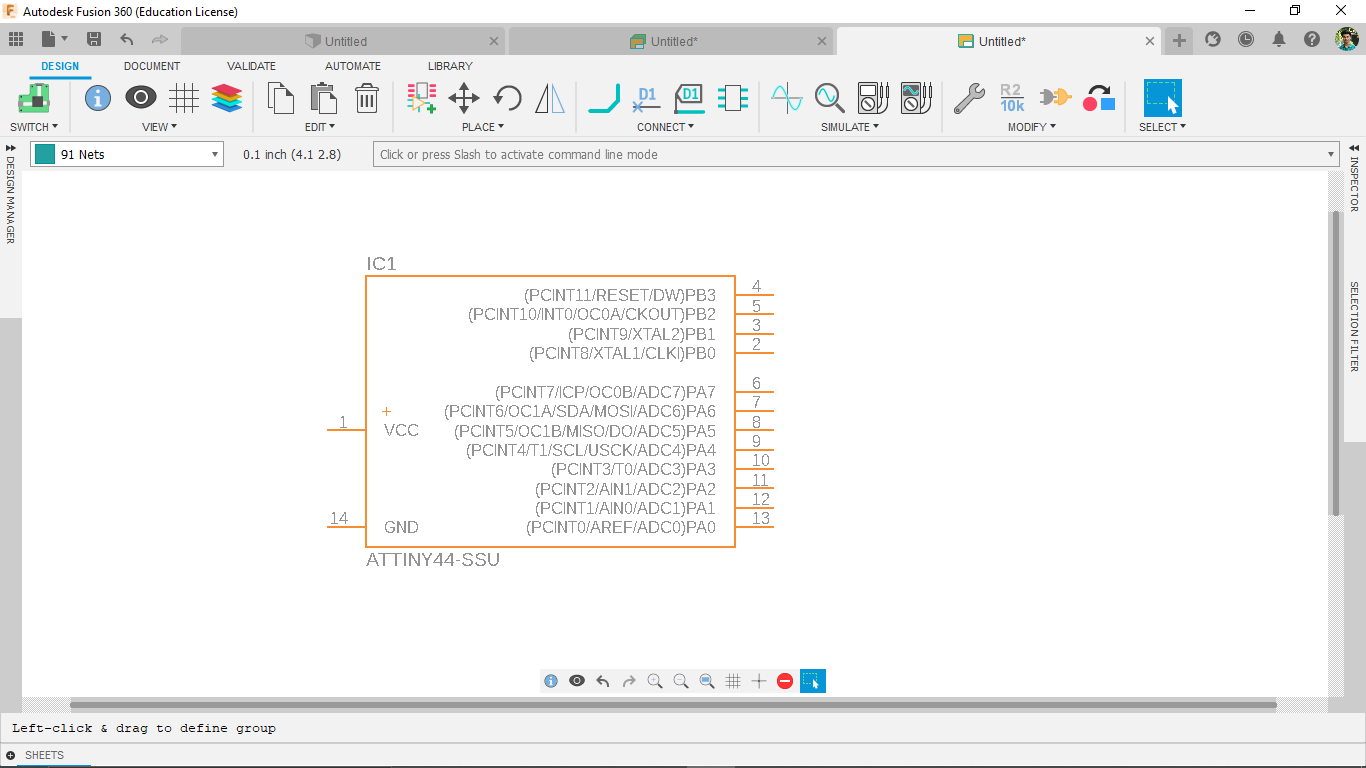
After adding the Fab Eagle Library successfully I started to draw the Circuit Schematic,Started from adding the main component The Attiny44 Microcontroller
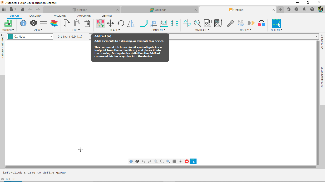
For adding a part I clicked the on the add part tool which opens the library components.there is another way to use all the tools,That's by the Command line by clicking '/' key the command function will activate then type the command for example to adding components type 'add' then click enter
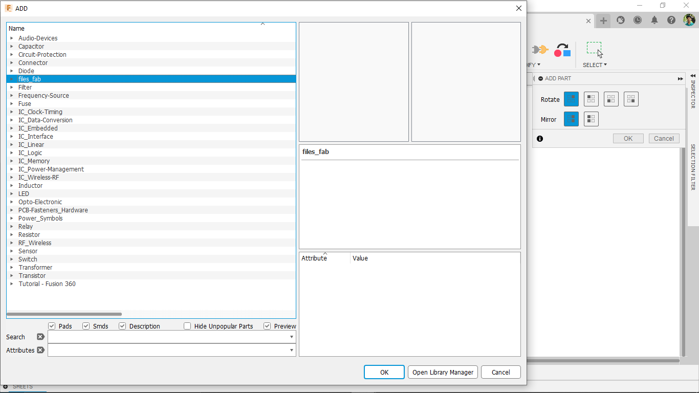
then I expanded the Files-Fab library package and found the Attiny44 Microcontroller SMD Version
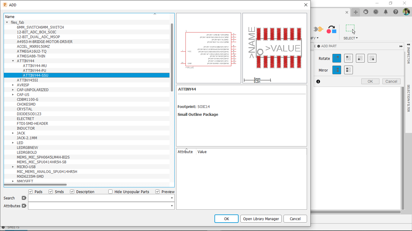
I placed the attiny44 pin daigram on the center of the work space
This is how Adding part in the E-CAD,Then I added every other components which includes 3 switches and 1 RGB LED ,3 Single Color LEDs and other components like resister,resonator,capacitors..etc..
Circuit Schematic
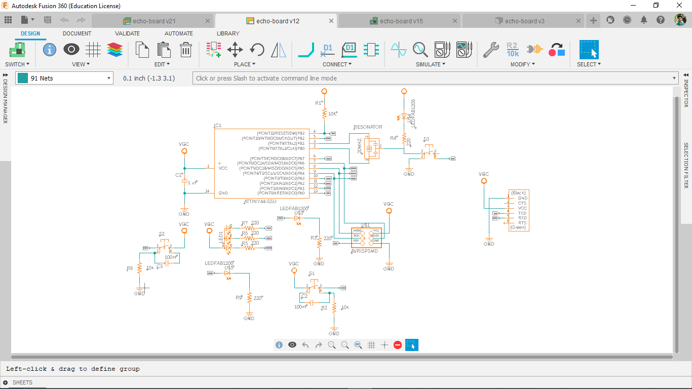
So I connected every components like I draw on a paper and one thing is missing in the schematic design.I usually add schematic Frames which helps to organize and document the schematic beautifully.
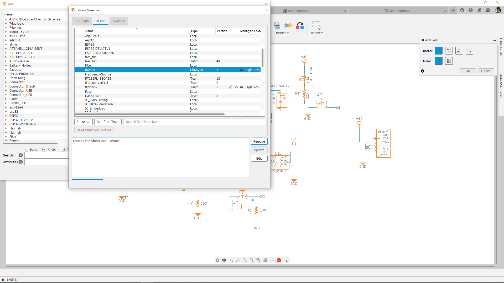
In order to add the Schematic 'Frames' I opened the library manager and searched for the 'Frames' Library from Fusion's Library under the Available Tab.and installed to my fusion cad by double clicking on it.
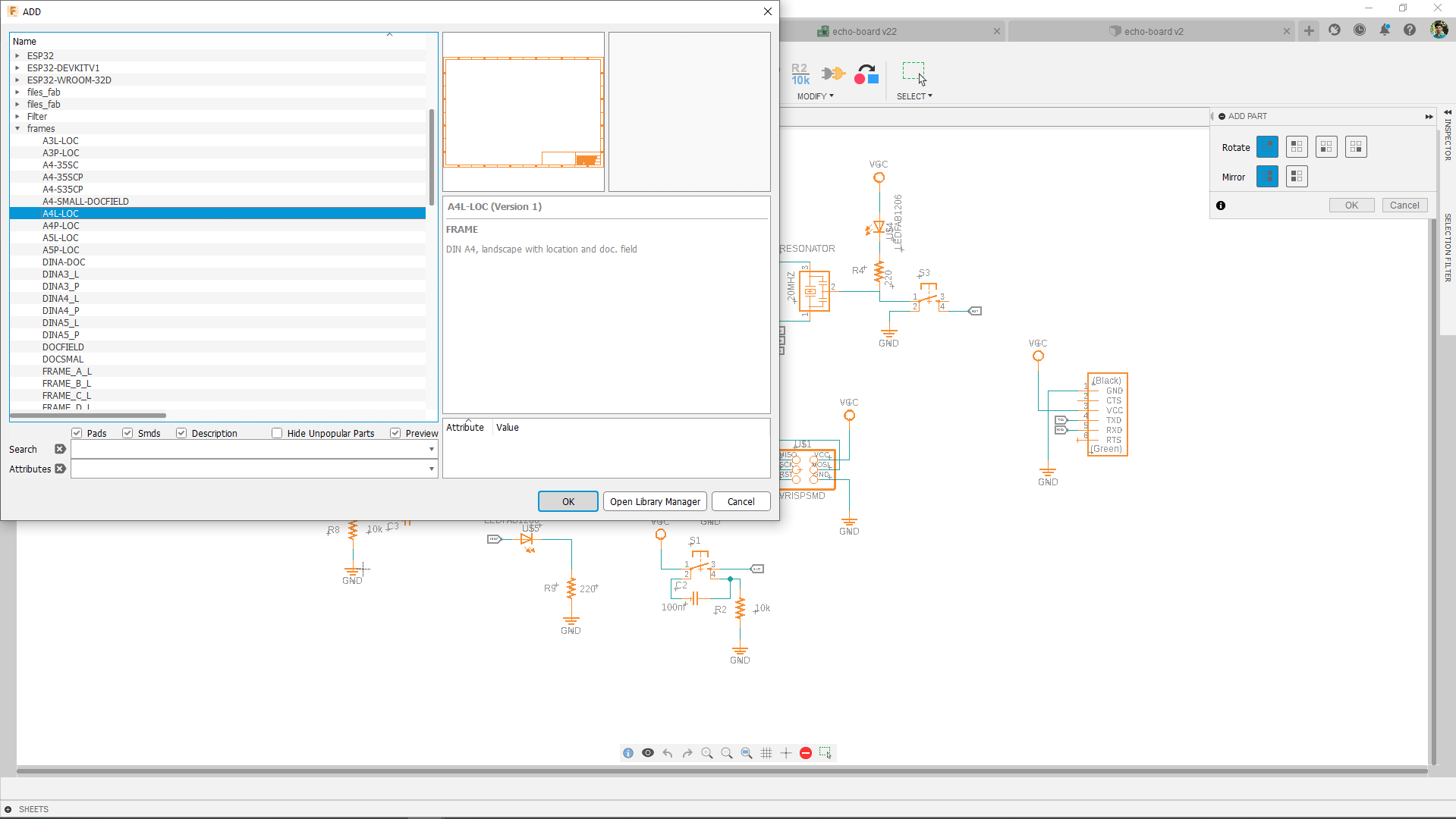
Then I added the frame to the echo board schematic from the library and arranged everything part by part
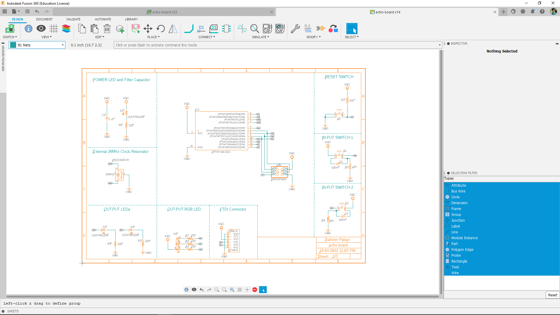
So I've Added the fame then arranged everything section by section as beautiful document. This way we can perfectly understand the design of each section and easy to navigate through.
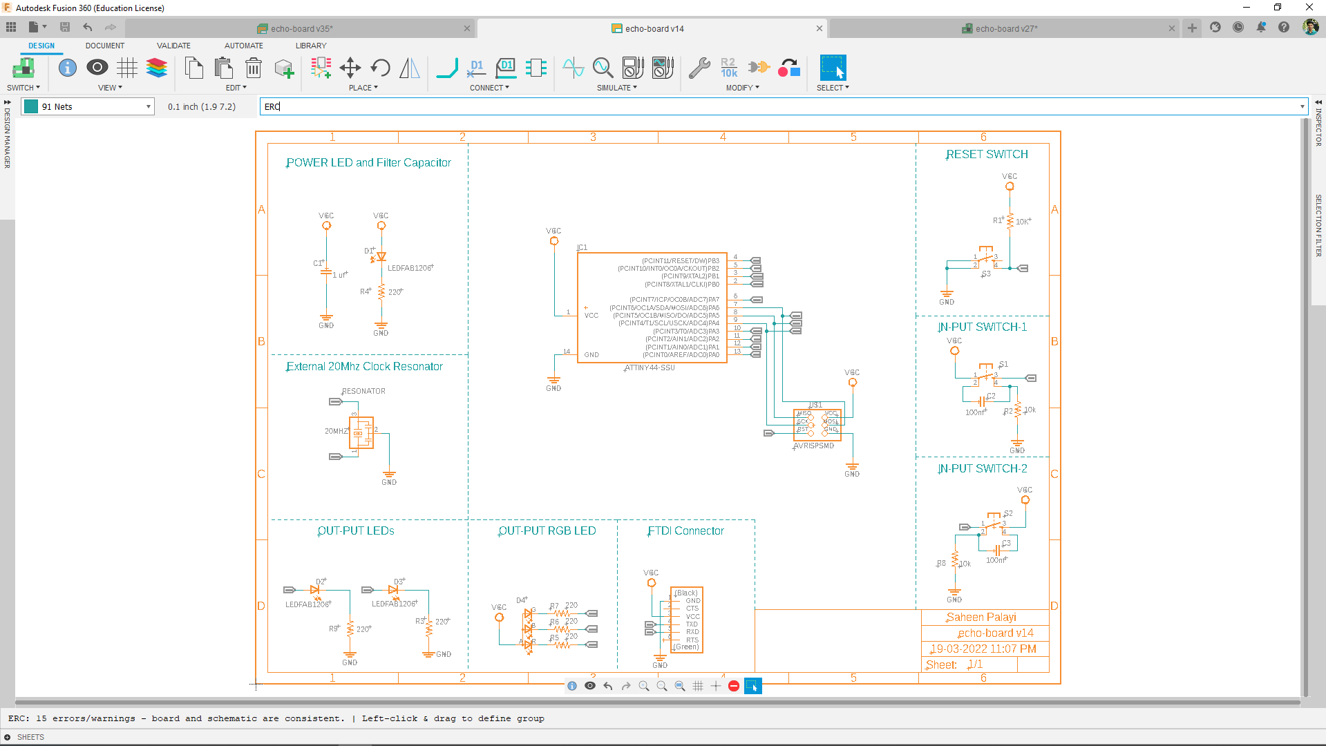
Now its time to do some Error Check by typing 'ERC' in the command line.Thais opens a new mini window showing errors and warnings if any.
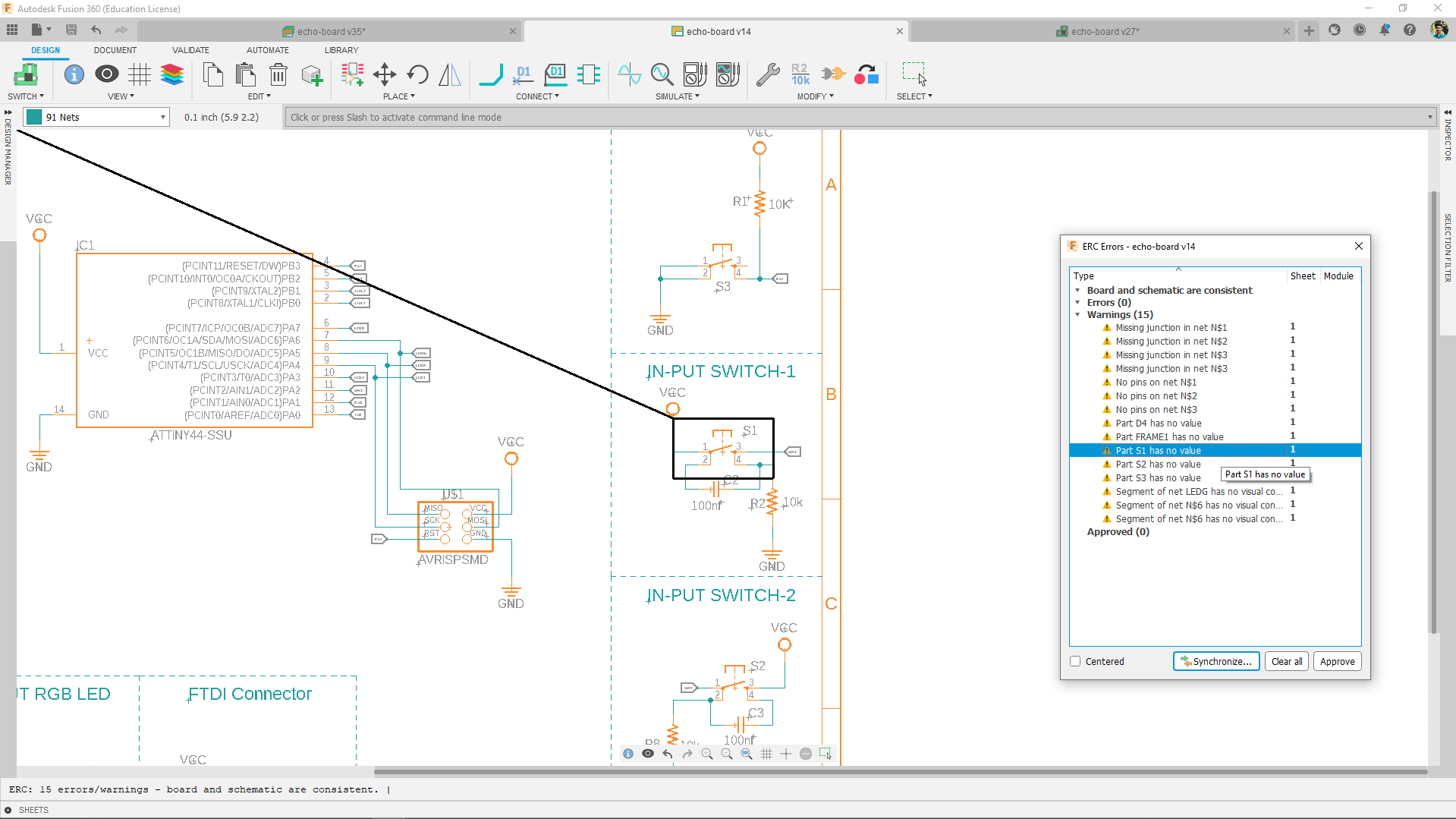
I didn't get any errors all I got some warnings that's not gonna cause the entire circuit from making the PCB.
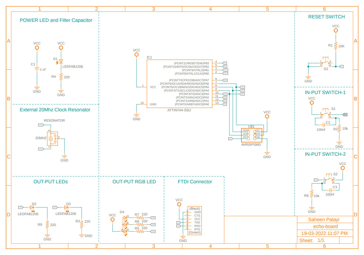
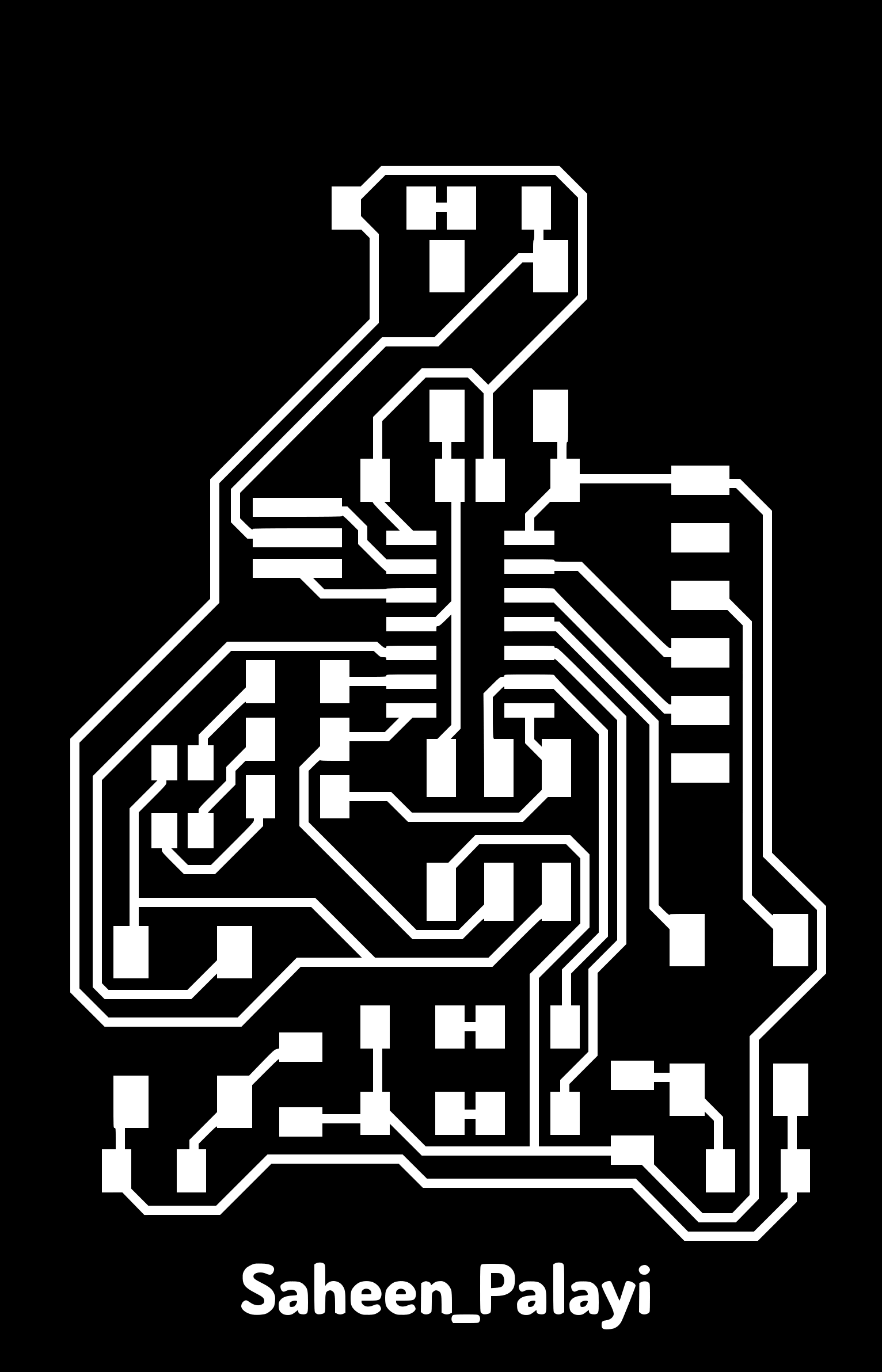
Here is the final diagram fo my Echo hello world and ready to convert to the PCB.
PCB layout
After creating the Schematic Circuit Diagram clicked the switch PCB option in the window's top corner.A new PCB file where created and opened in a new tab
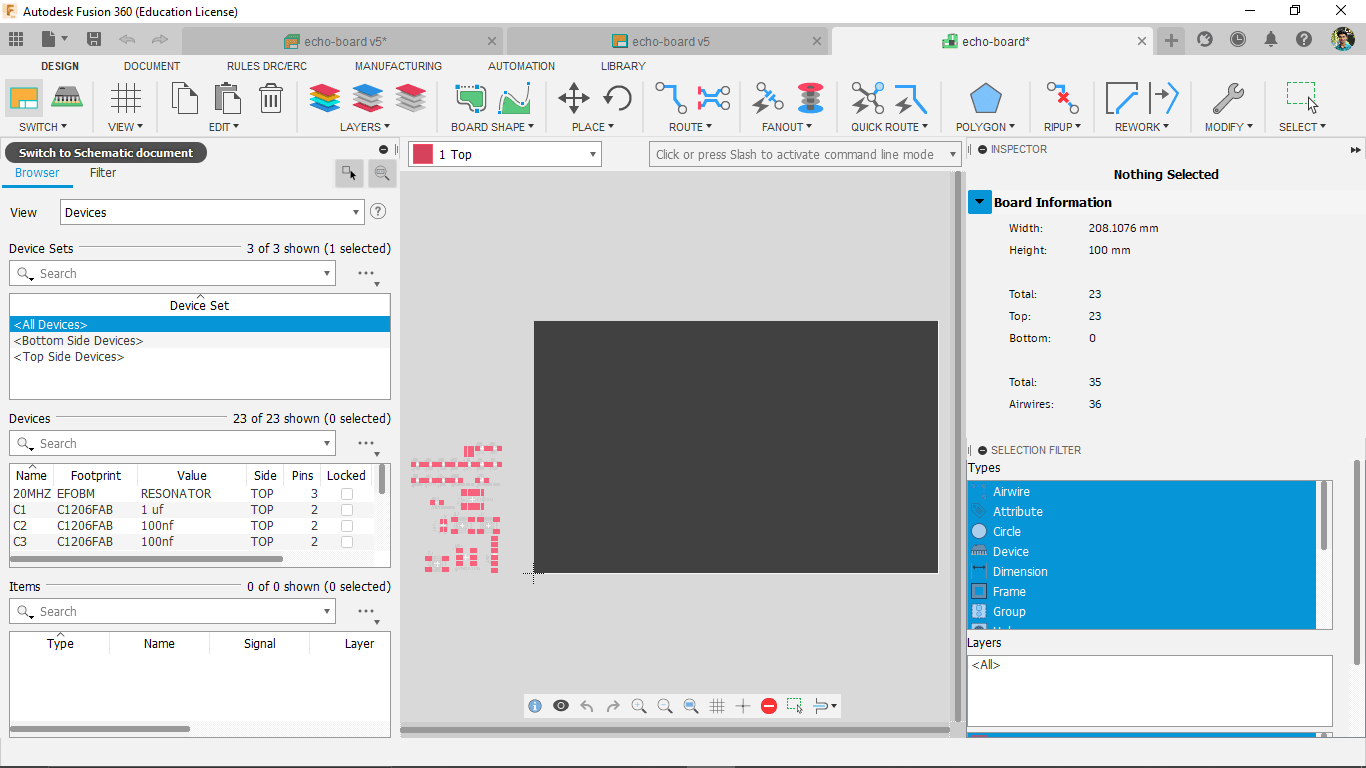
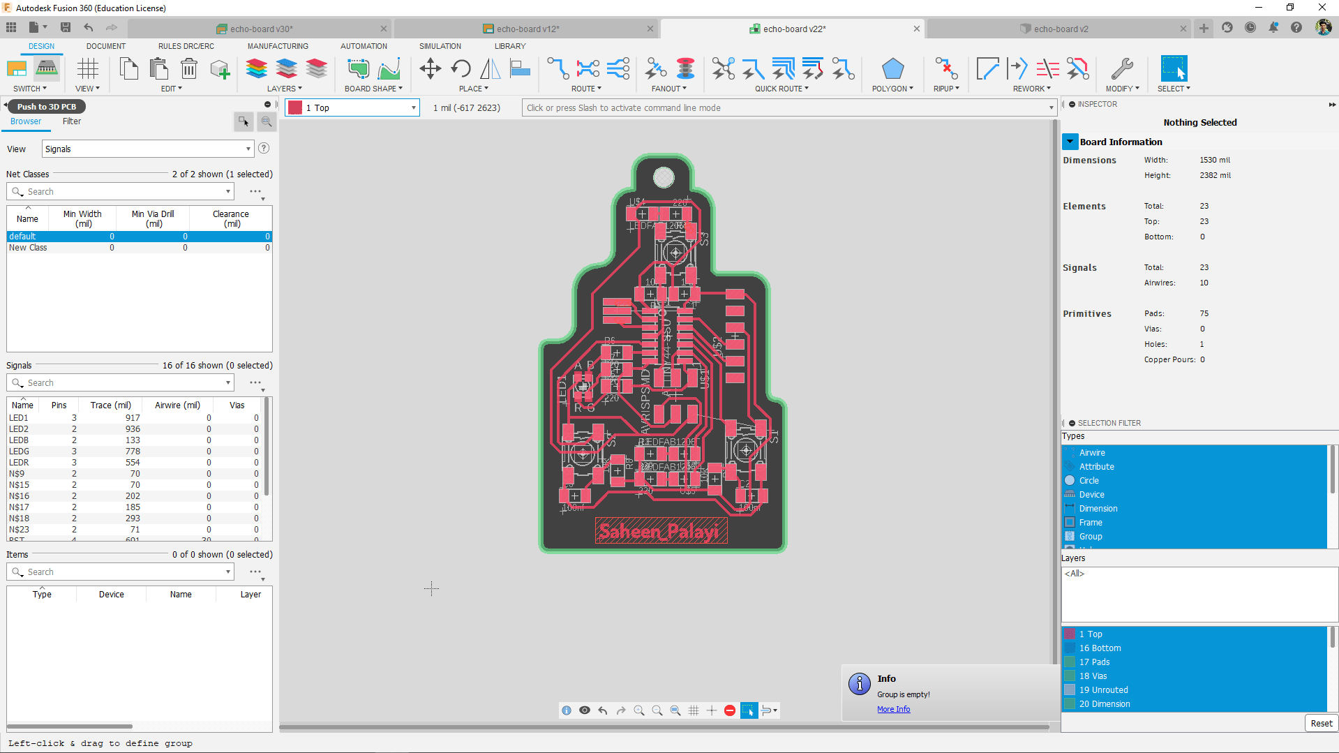
that converted all the circuit component into the trace pads on the PCB Top Layer with un-routed network path representations .That can be helpful to arrange the all the component according to the circuit with possible trace path without any trace crosses
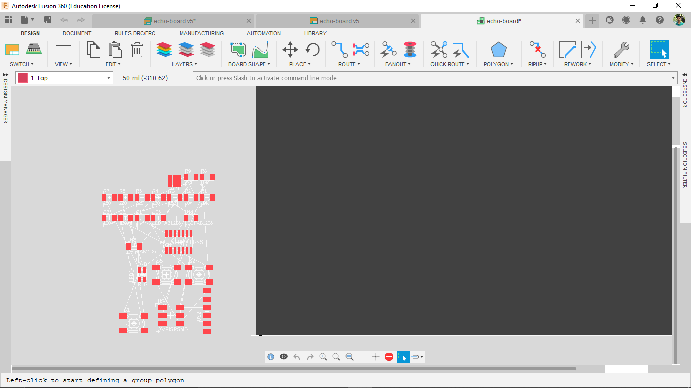
The black area is the PCB working Environment now that's the whole PCB.I selected all the components and dragged into the black Colored PCB area
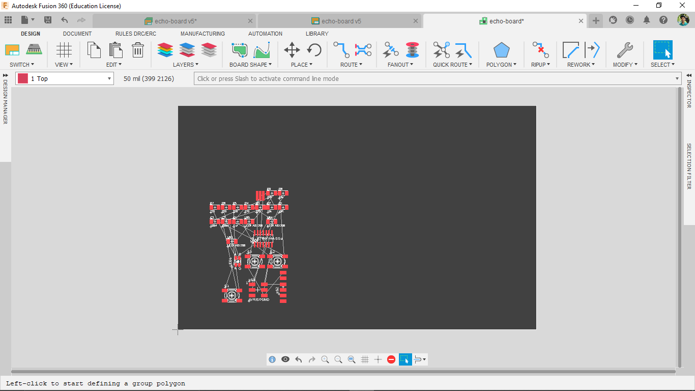
Then I started to arrange the components in a possible way like the un-routed reference paths not crosses I's better to do like the sample echo_hello_world board see the echo_hello_world board that provided by FAB

I arranged all the similar component like Neil's board.That made easy to arrange everything.then I also aligned my input output components pads
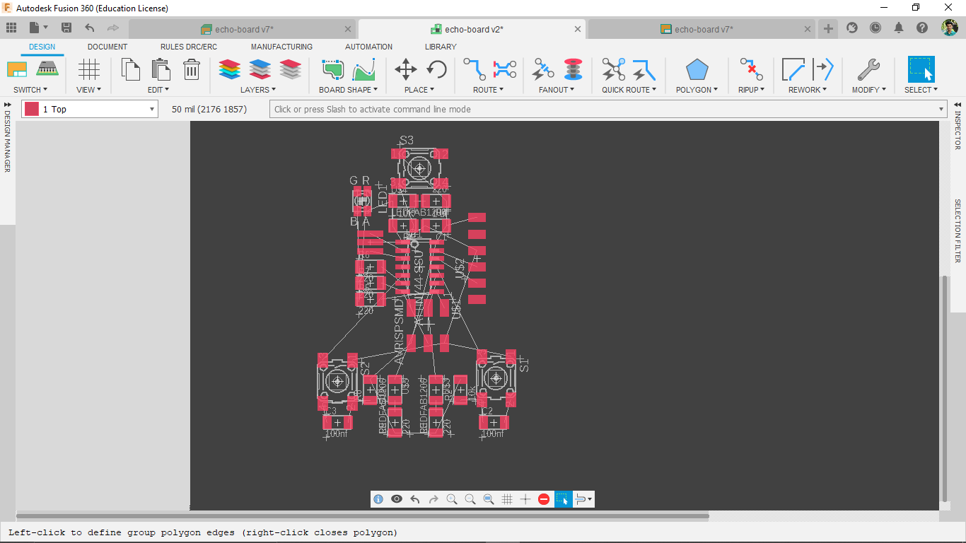
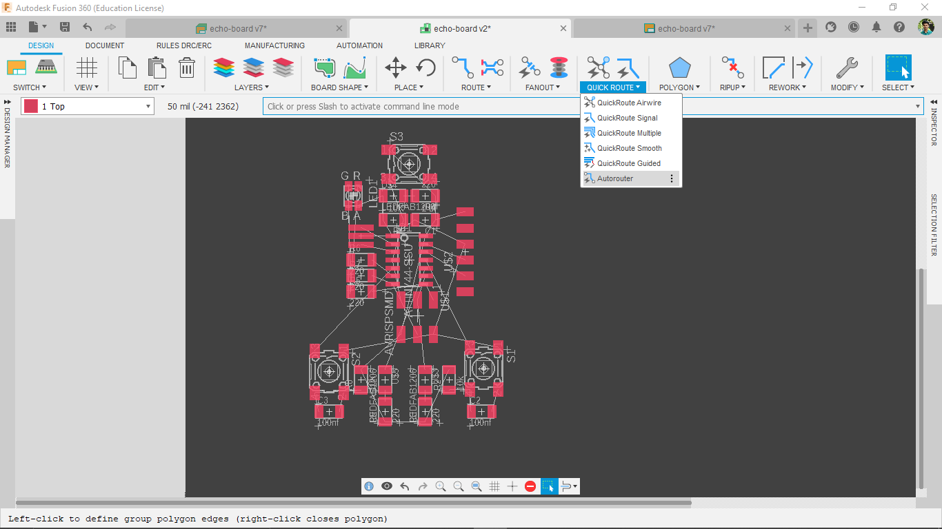
Now I have to route all the part for creating coper traces or tracks between the pads.so we can do this track routing either manually or there is feature available called auto routing
before doing autoroute I calibrated the design rules for the PCB tracks found the rules on DRC menu under rules and DRC/ERC tab
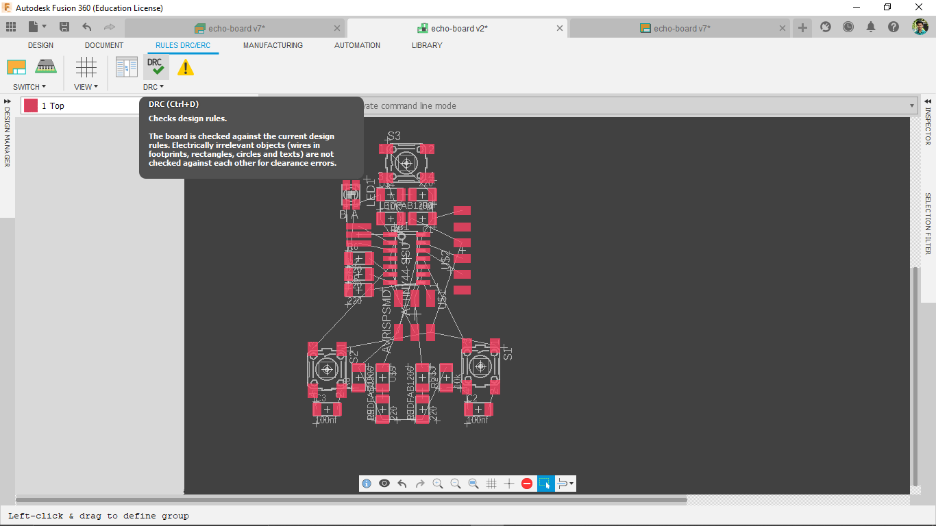
I clicked on it then it opens a new window of setting of rules for checking the PCB traces
In FAB LAB we are using a 0.4mm (1/64") milling bit four routing the traces for PCB so in Inches its almost 0.015625 inches so round of 0.016in which means 16 mill
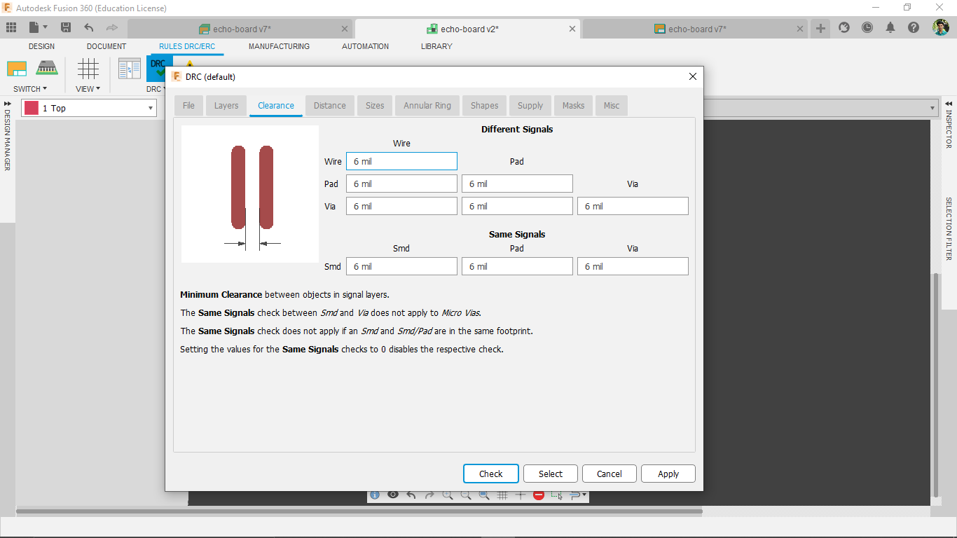
Moved on the clearance tab on the DRC window.every clearance there was set for 6 mill.It's ok for other method of manufacturing like Chemical etching
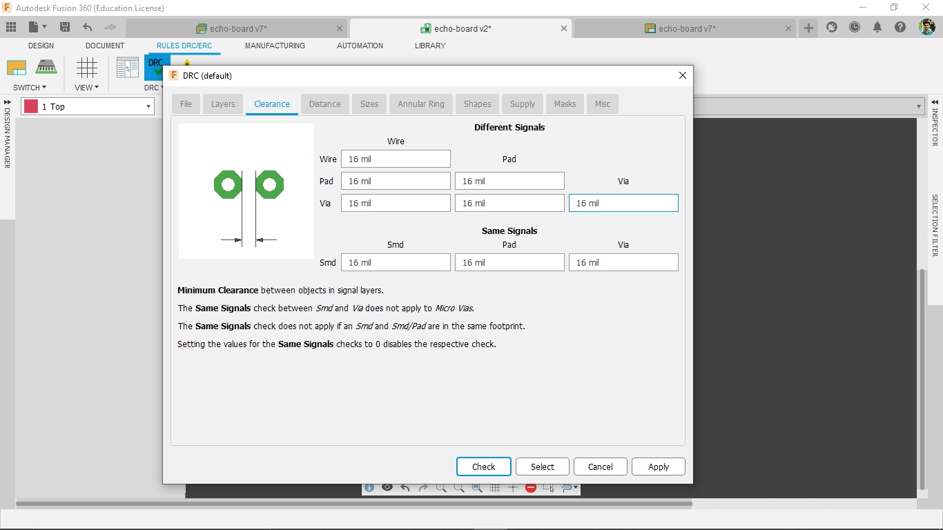
I changed everything there to 16 mills next moved on the Distance tab for changing the trace distance
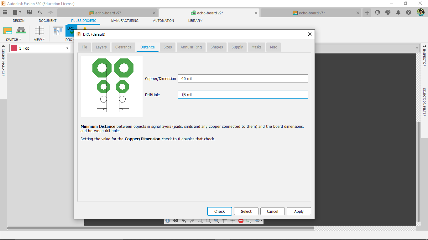
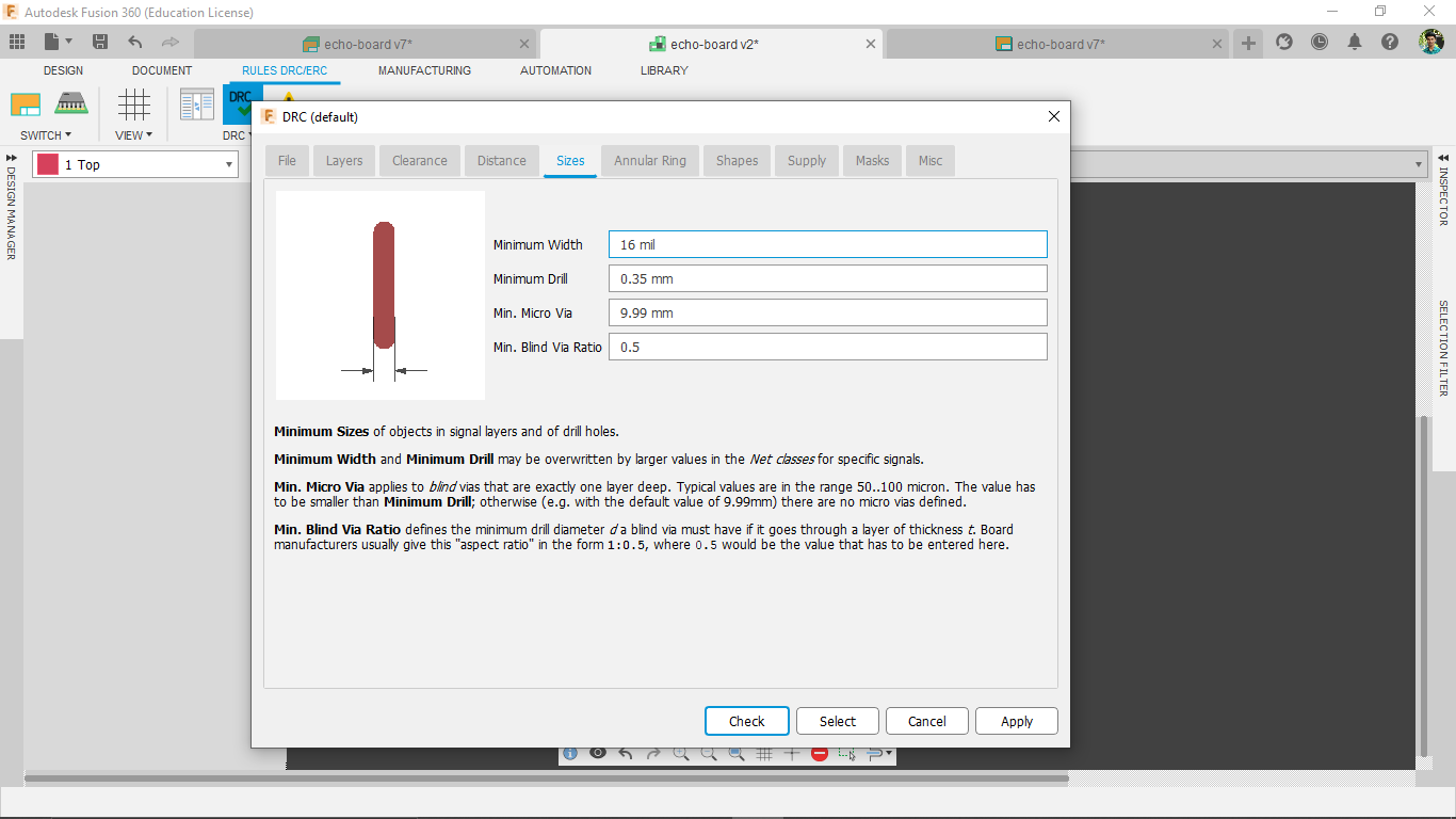
After changing the trace Distance to 16 mill moved on other tab called Sizes for setting trace width.changes that to 16 mill as well
Then clicked apply and exited from the DRC window and opened autoroute tool that opened a new window with routing setups
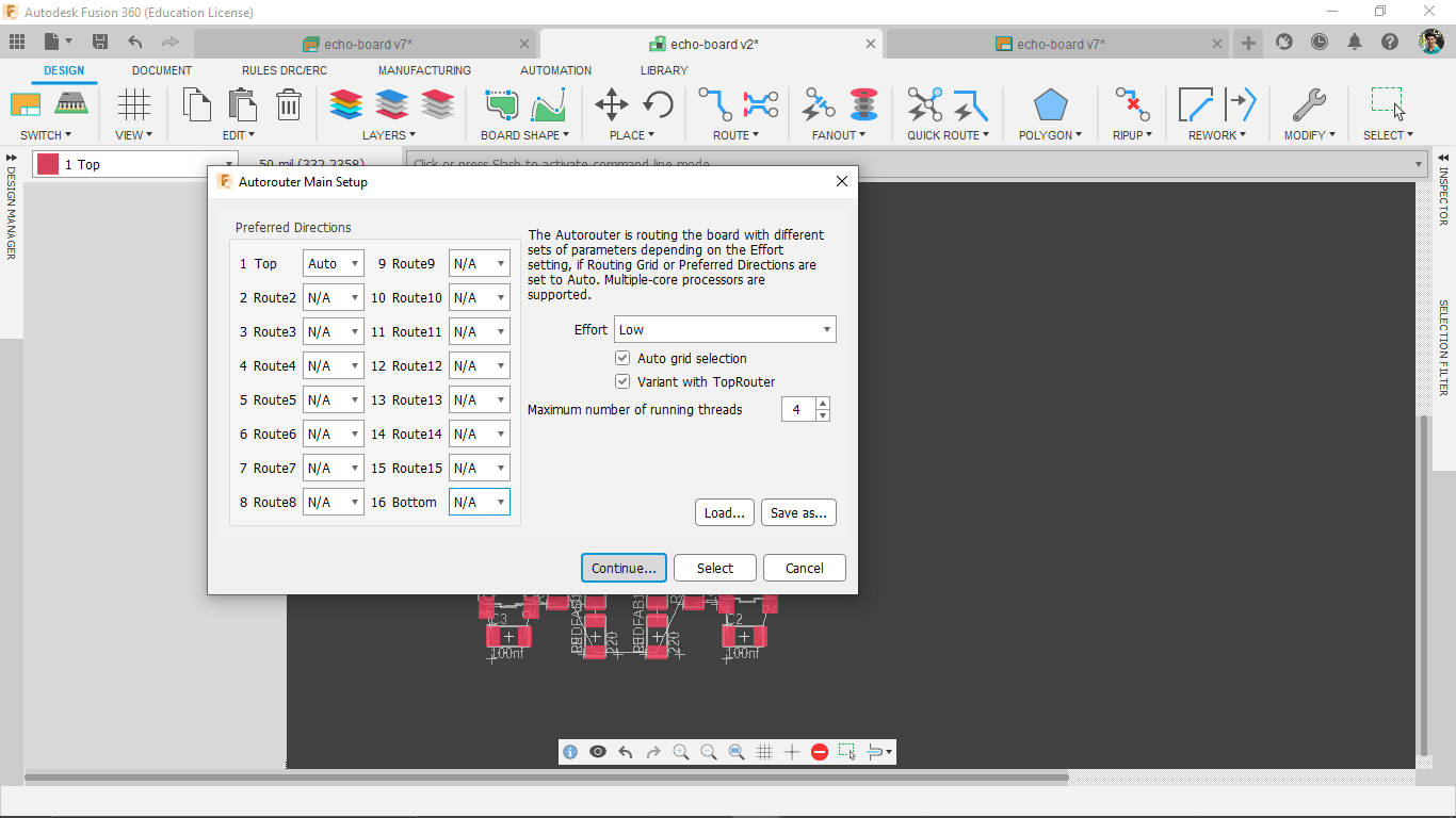
Disabled all the layer selection to N/A and activated Auto for TOP layer becouse we are doing SMD PCB with a single sided copper clad PCB
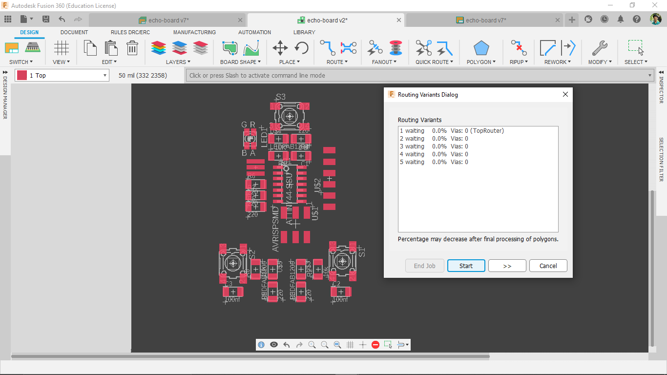
After clicking continue goes to a routing menu and I started the job
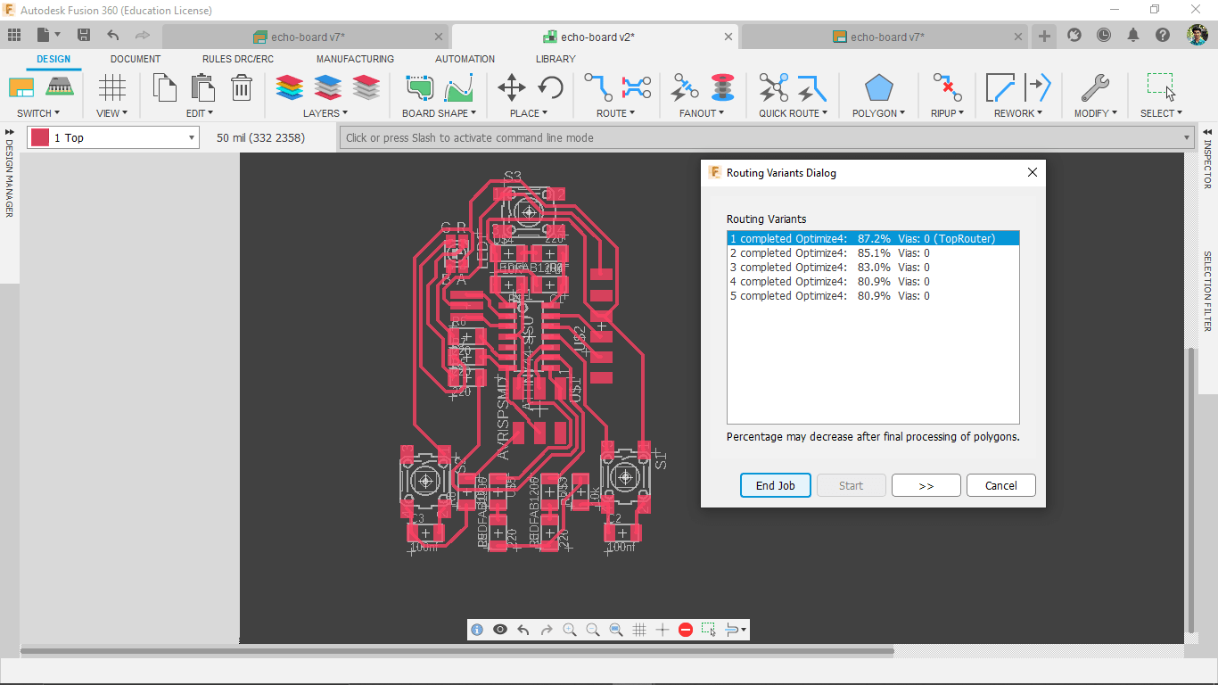
I got 87.2% job done for routing the tracks with 16 mill clearance,width etc... .So I need to rearrange some components for a better routing result
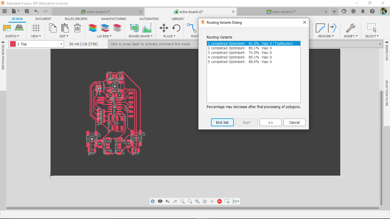
I rearranged some components and routed again got 91.5%.I have to try again..
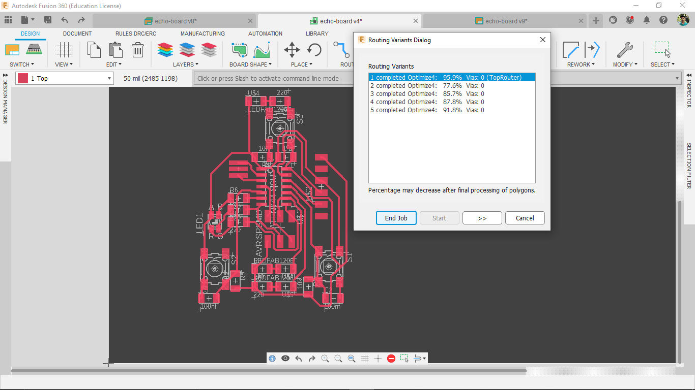
Modified some schematic and did the routing again.this time I got 95.9% successful trace routing,but still not 100%
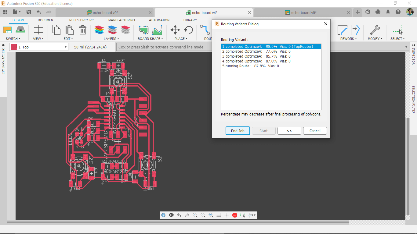
I did the process over and over again then got 98% success.Then I Evaluated and stopped the auto routing and started do some manual routing and also some manual adjustments
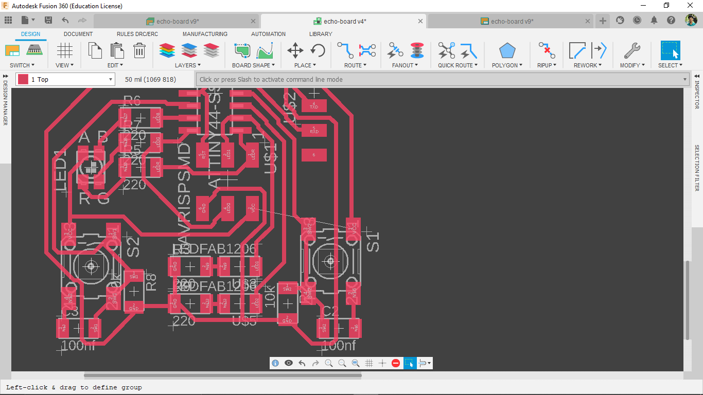
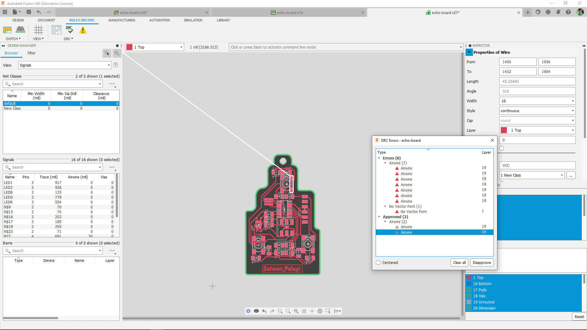
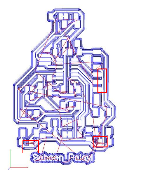
The above picture shows the un-routed part which not routed byt the autoroute tool.The switches have 4 pins and 2 contact which means 2 of them connected in series.so,I used the switch contacts as a track over the under trace that fixed the problem
I got complete circuit which works thanks to my experience in PCB Design also and thanks to the fab instructors.Practice makes to solve things in easier ways
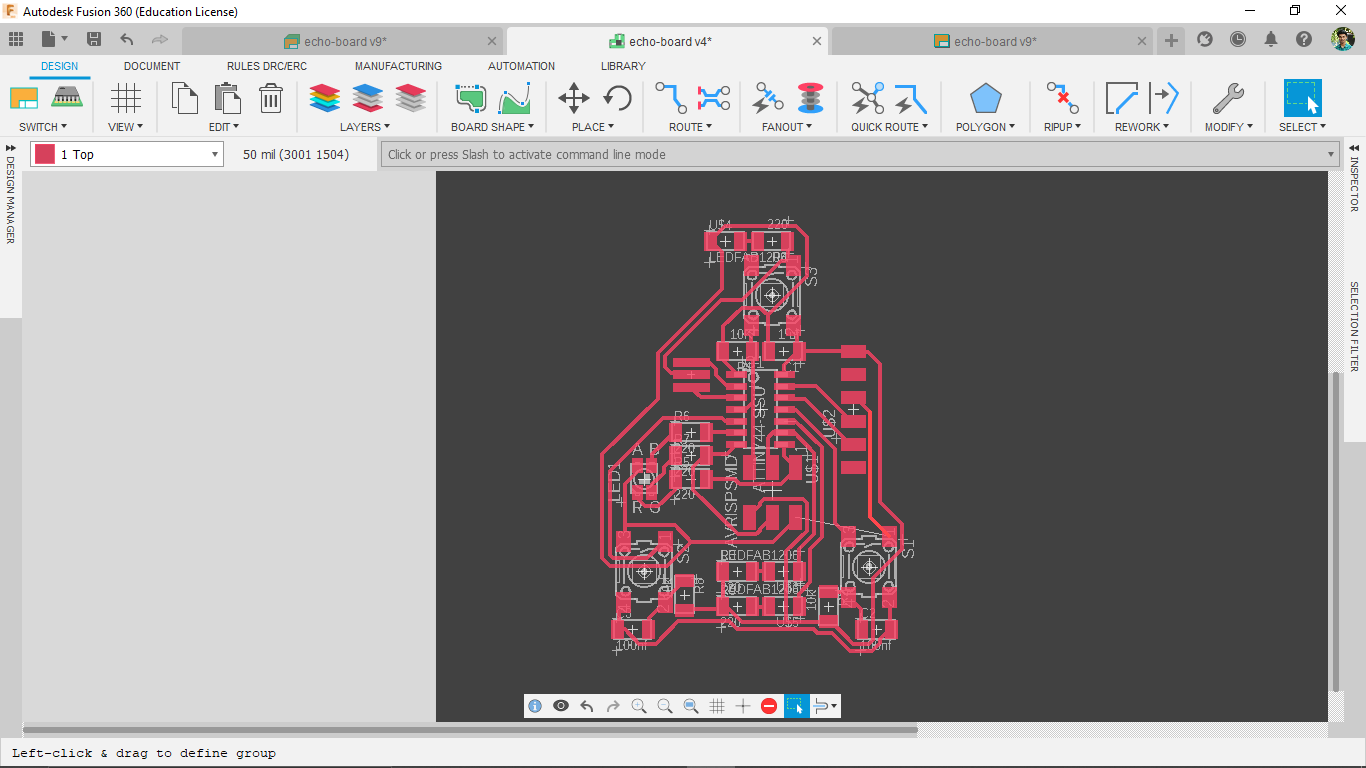
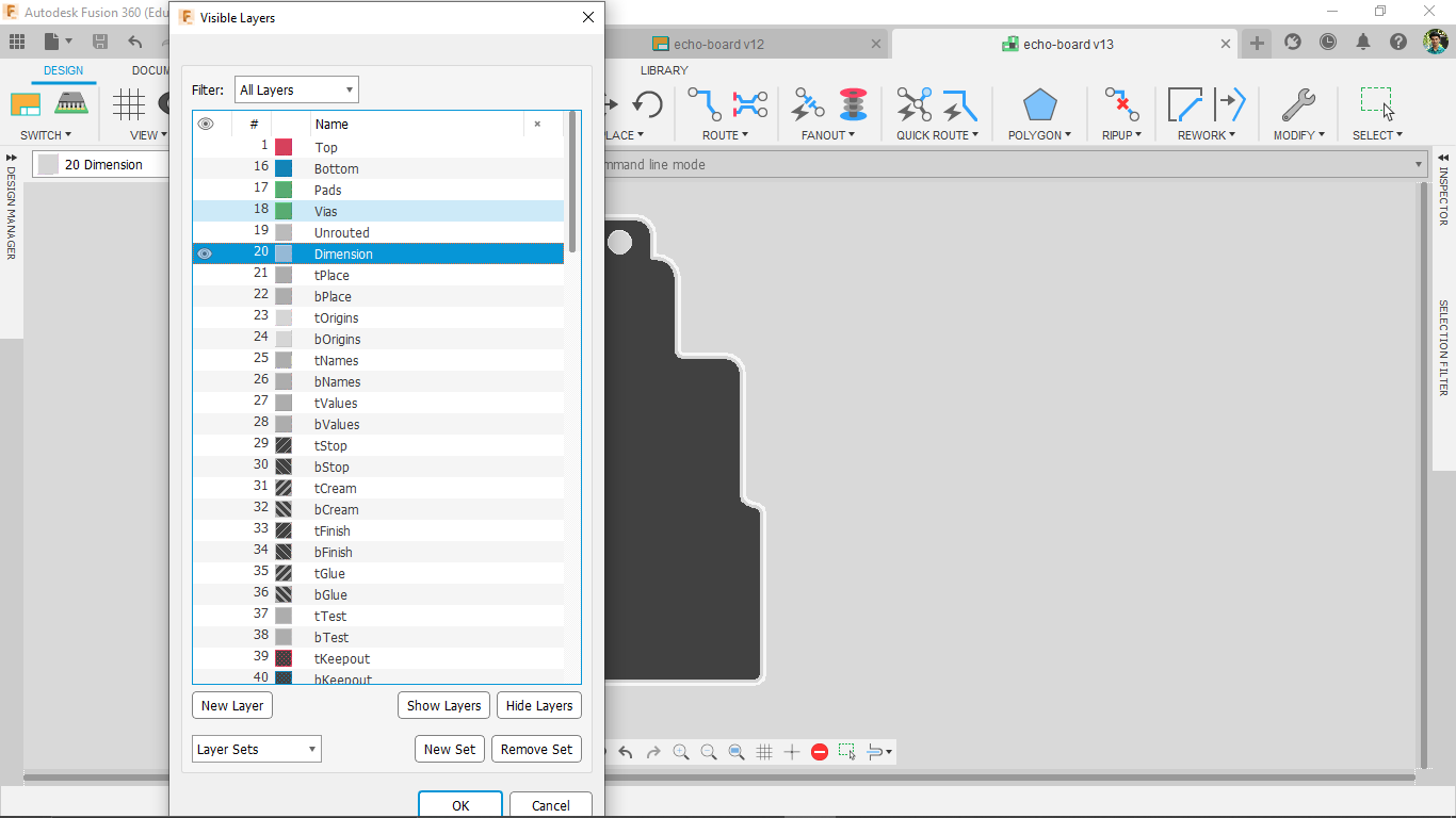
Now I have to adjust the out line on the dimension layer for making the pcb boarder that also reduces the black area.I know how to make square PCB's ,for a change I decided to go with a random curved corner shape drawn by hand with vector border line
Hidden the whole layer except the dimension layer and selected the whole pcb by dragging over it and deletes the rectangle structure
Then i drew the dimension line in 32 thickness and activated hidden layers back got a locket badge shape PCB
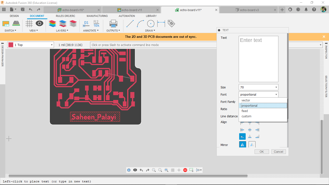
now I wanted to add my name on the PCB for milling out as a coper traces so using the text tool from the fusion e-cad I wrote my name with custom font
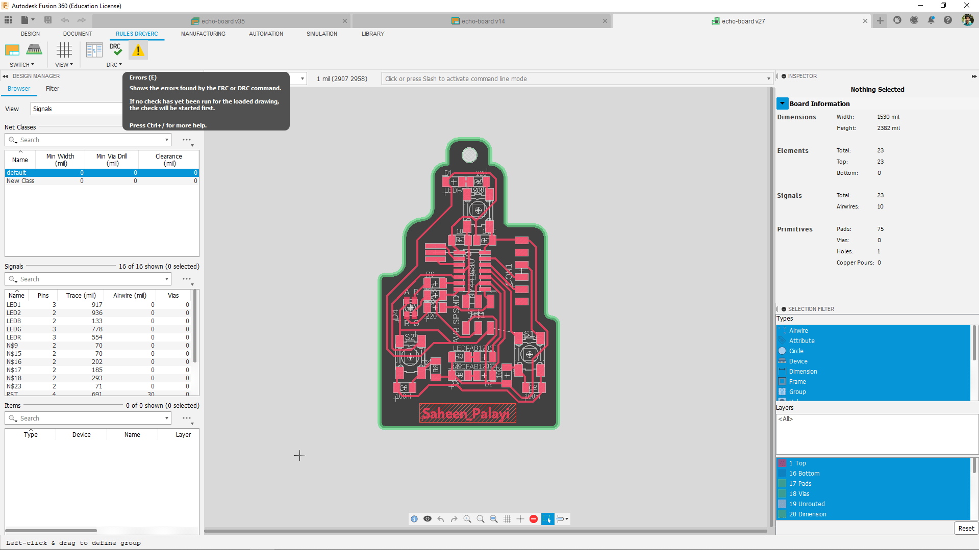
It's time to do error check in my PCB design by clicking the 'Errors' icon under the RULES DRC/ERC.
Just like I thought I got two expected errors and few warnings . The errors on the un-routed wires I left by which will connect through the switches so that fixes the problems. And the warnings I just Ignored because it's oky for this now.
Exporting for milling
My PCB Design is completed ,now I have to export the file for milling
The file should be in PNG format or SVG so the most of the Electronics design cad provides PNG.I need two different files one for cutting and other one for tracing
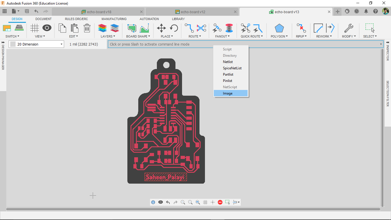
on Command line I entered 'export' and then I selected image export option
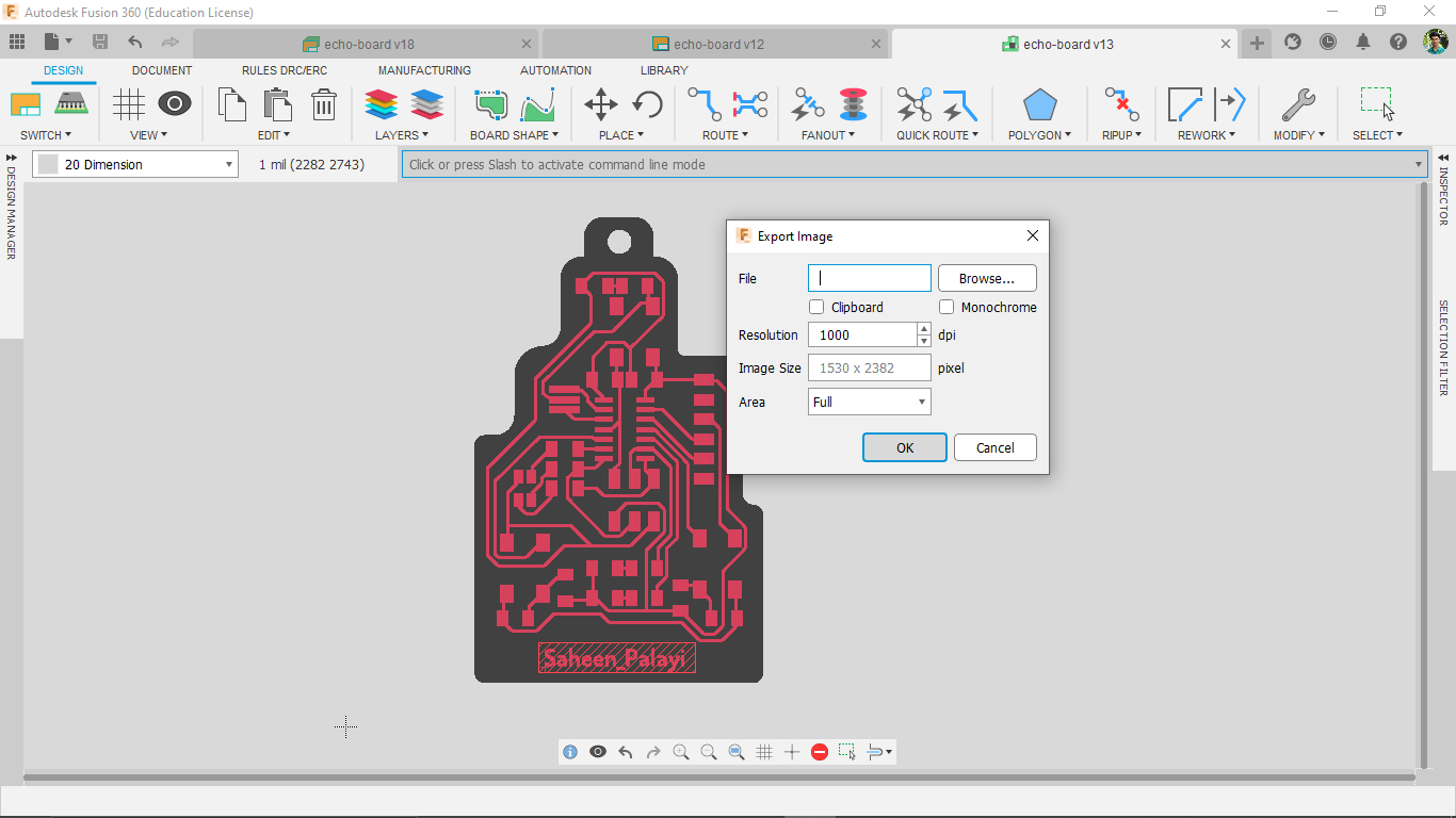
I gave 1000 dpi and gave a file name and location then I clicked ok
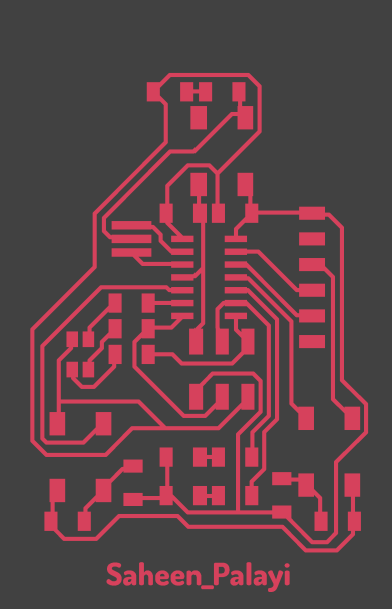
But i need the image in Monochrome .While exporting there is an option for Monochrome but it seems there is a software issue with the fusion 360 Electronics CAD.then I used the Inkscape to trace bitmap out from the image
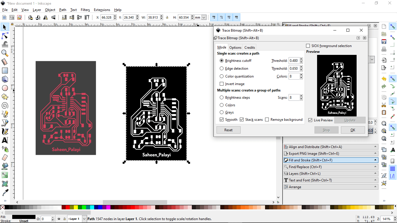
The converted vector image exported to pngs and also saved in SVGs(for testing SVG)
Then I opened the desing in FAB mods and observed the tracing path simulation
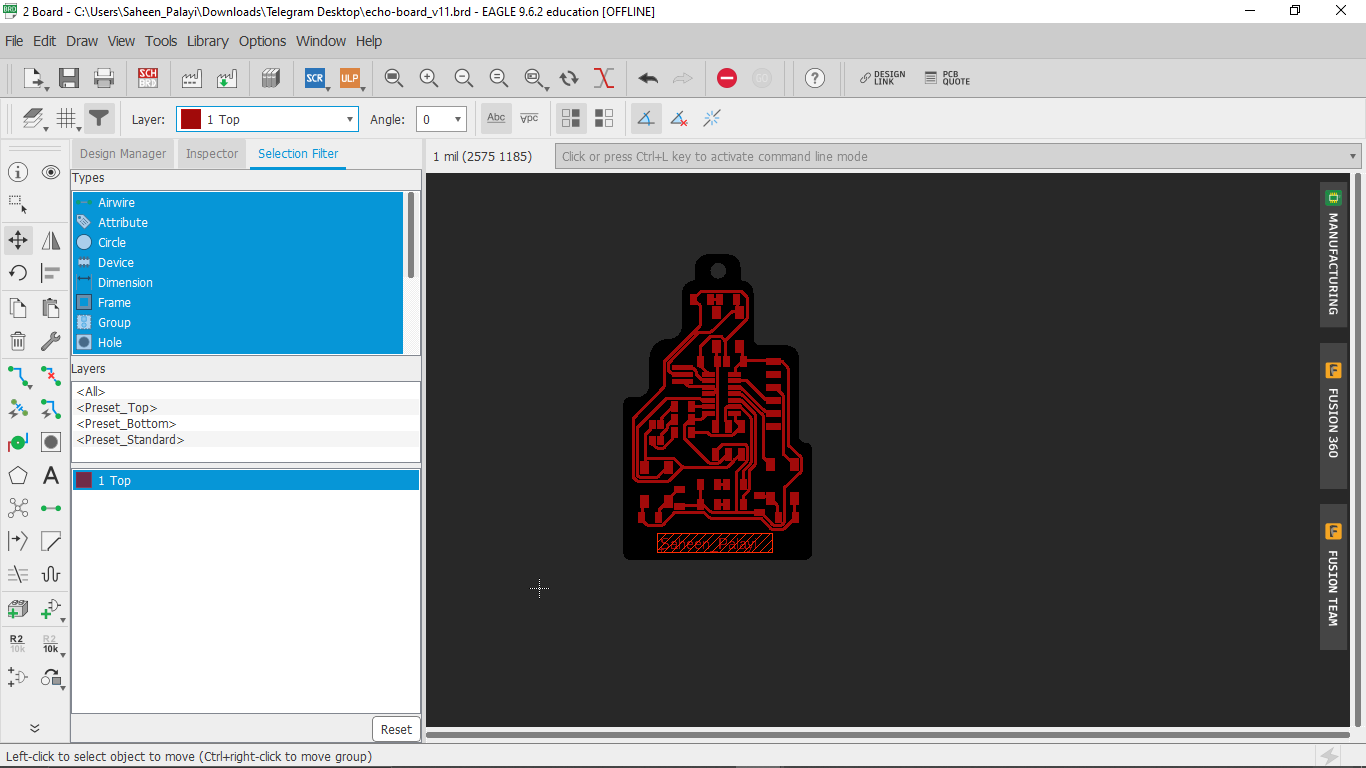
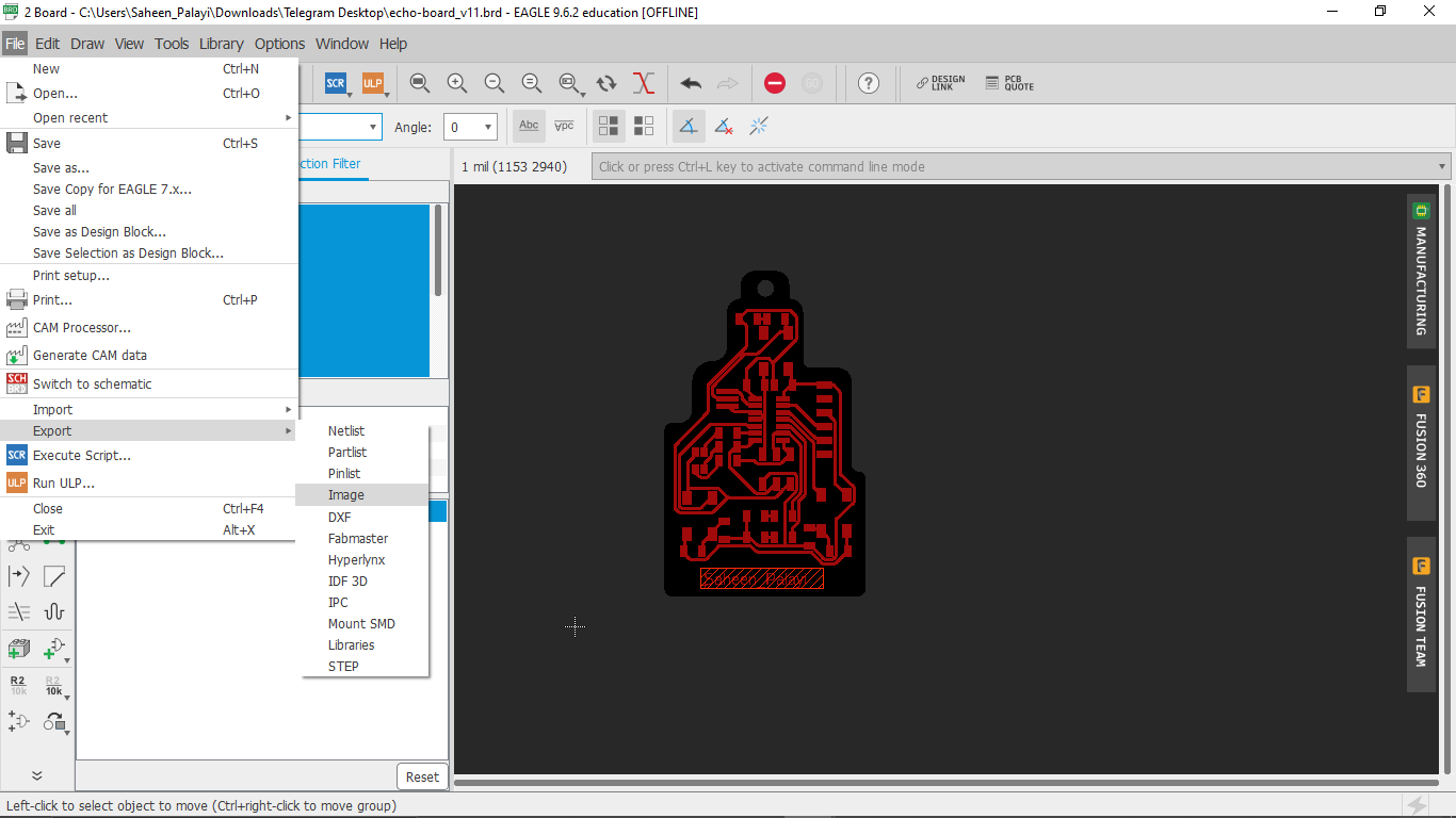
I spotted many error that trace gonna contact in the result which don't wanna contact together so turns out I have to edit,export and also need to do the Monochrome conversion agin.So I exported the board from Fusion 360 to .brd eagle files and opened in eagle
I hide all layers and opened the Image export window by following File>>Export>>Image
Then I entered everything like I did in the fusion and also checked the Monochrome for saving the png in black and white then I got the Monochrome output. But using two different software to just get the results is hard. While I'm following this procedure one of my instructor show me another way.
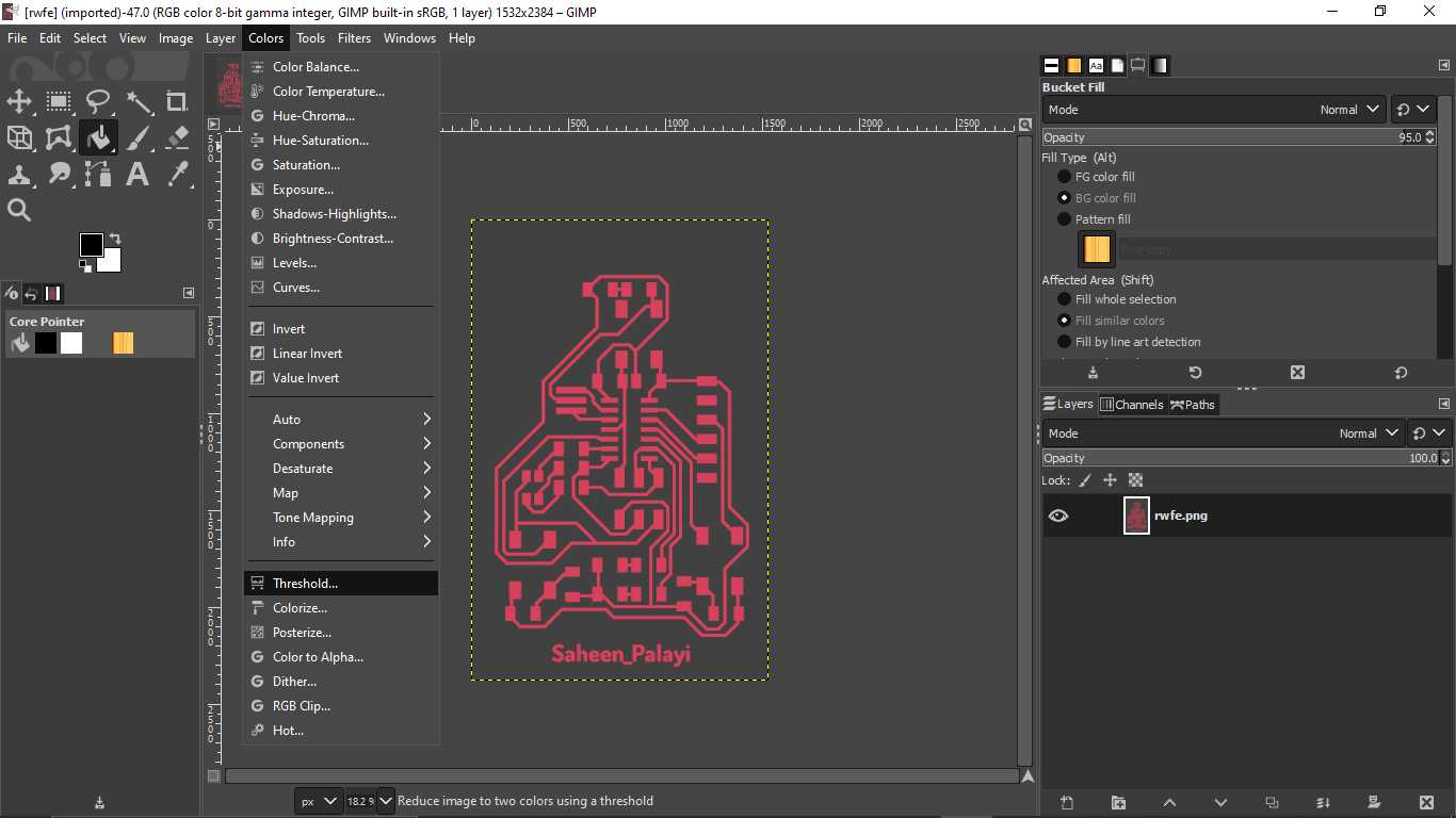
To convert the output png from fusion 360 electronics CAD to Monochrome just opened in the GIMP image manipulator software and just clicked 'threshold' under 'Colors' options.
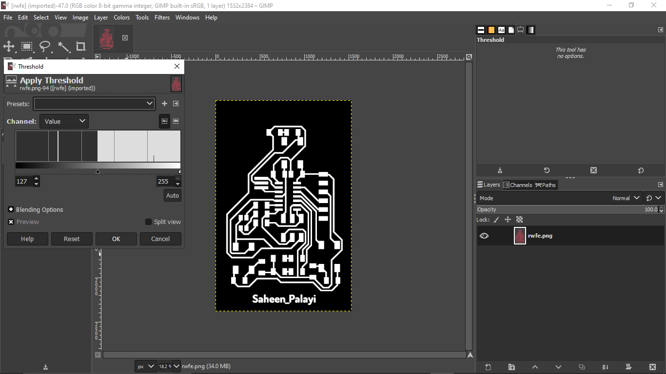
Then it changed to Monochrome and just clicked ok to finish.After that I exported as PNG without reducing quality. Also possible to overwrite on the existing PNG file.
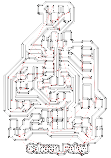
And then I calculated the tool path again in mods for checking any short paths after the milling. Got good tool path after all and it's time to mill it out.
Only the trace file is exported also required the cut file(the outline). I selected the dimension layer only to export the PCB outline and then saved as in 1000 dpi PNG form.
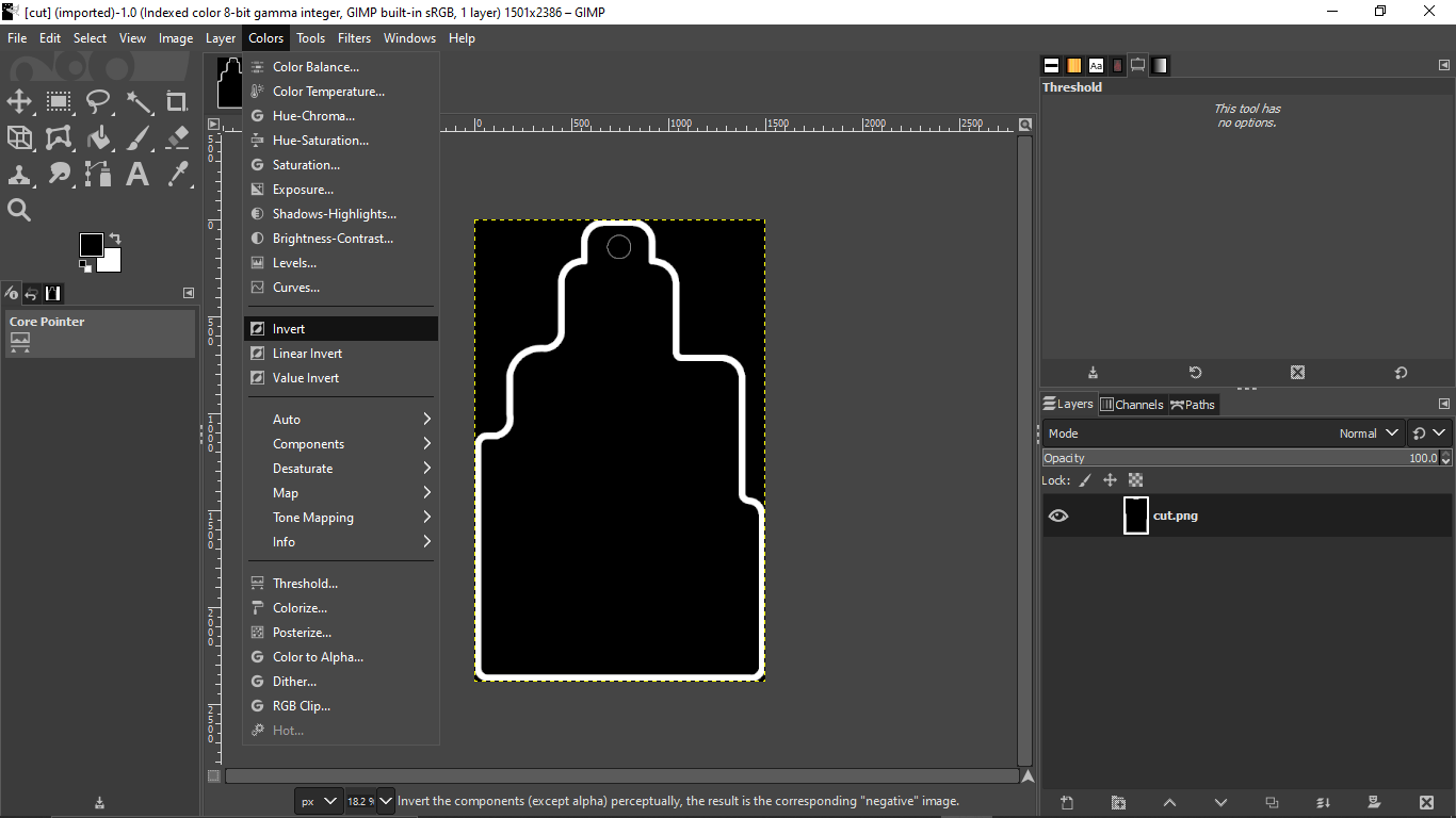
Then in Gimp I converted in to Monochrome and inverted the black and white color pattern by clicking 'Colors >> Invert'.
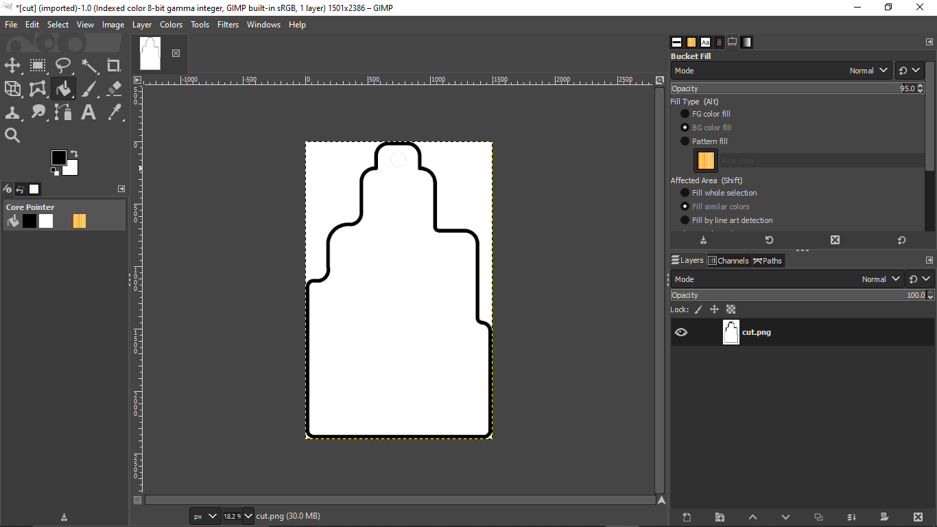
After inverting I selected the 'Bucket fill' tool and set the default color in black to fill.
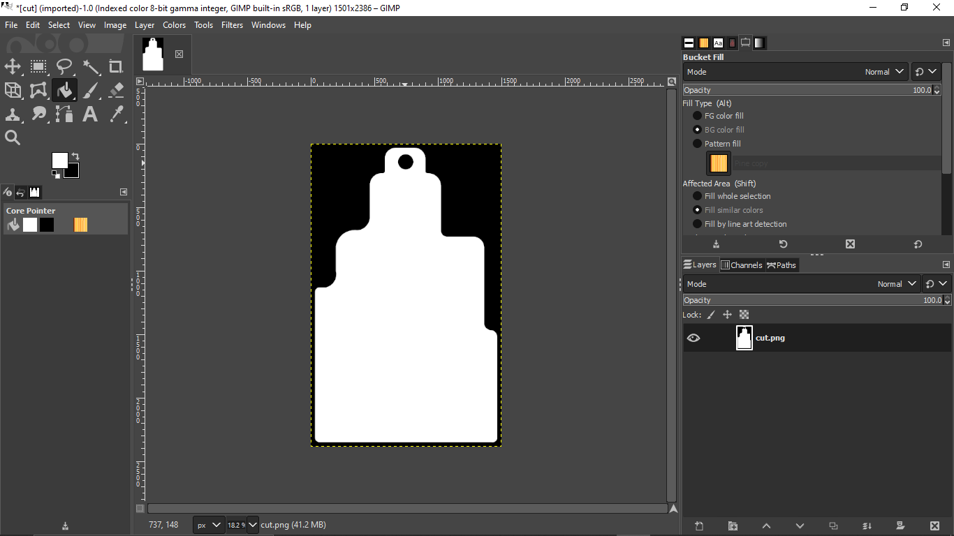
And then I filled unwanted parts which is out side of the PCB out line and inside the hole like in the above figure.

3D PCB in Fusion 360
Thi is is a fascinating feature in fusion 360 . we could actually convert the PCB into a 3D PCB Model that let us Intergrade in Fusion 360 3D designs like a electronic product design. this feature got my attention and I realized that I can actually create beautiful PCB's than the traditional PCB CAD Designs. For more Click here to watch the demonstration from Autodesk Fusion 360 Youtube channel.
To convert the PCB Design to 3D PCB I clicked the top corner button called "Push to 3D PCB" which is used to create or switch to 3D design.
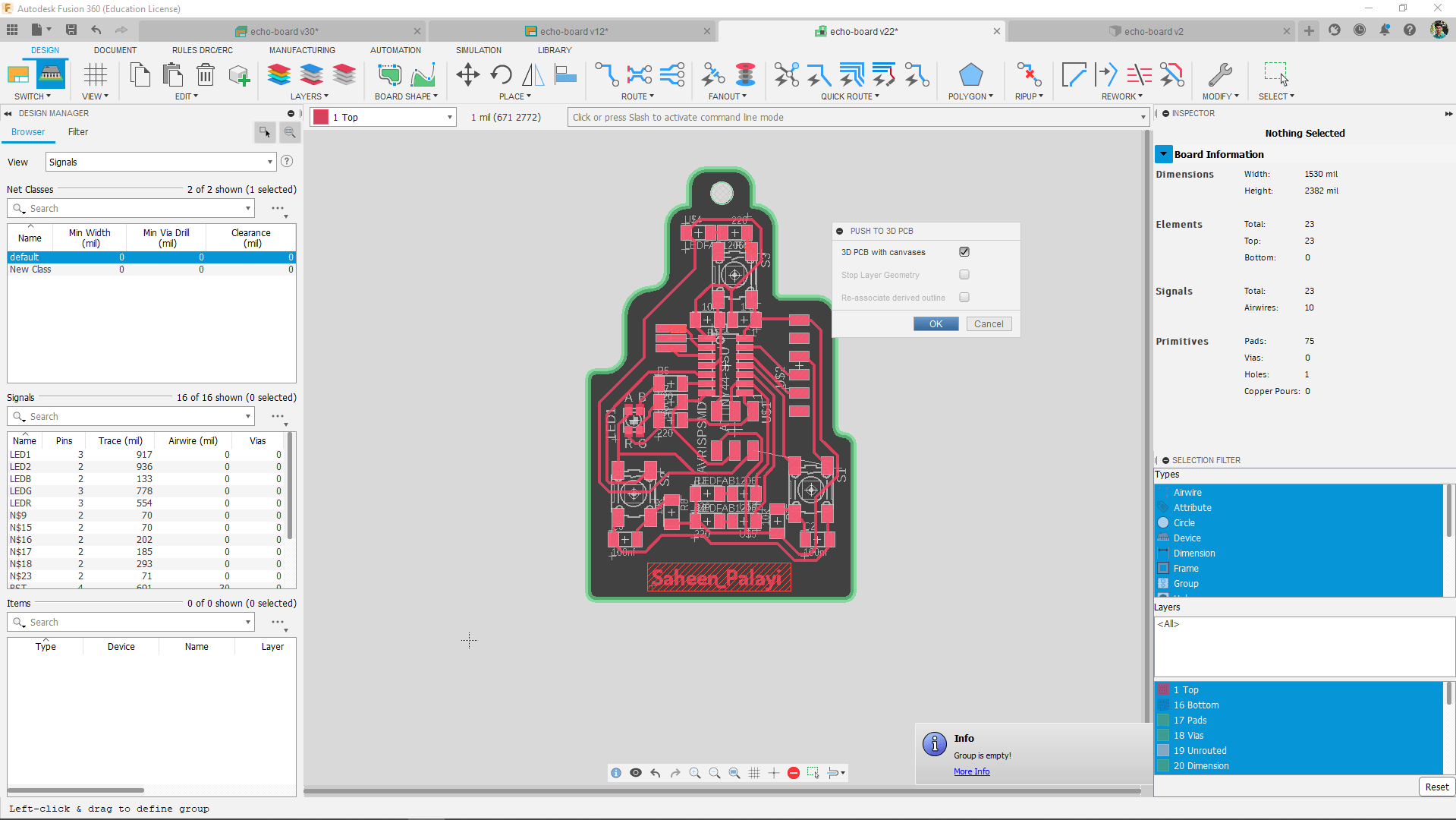
In the following window asked us to select an option in between 2 types of rendering options.So I selected the "3D PCB with canvases" option to create a low rendered 3D PCB because I don't want to crash my rendering.
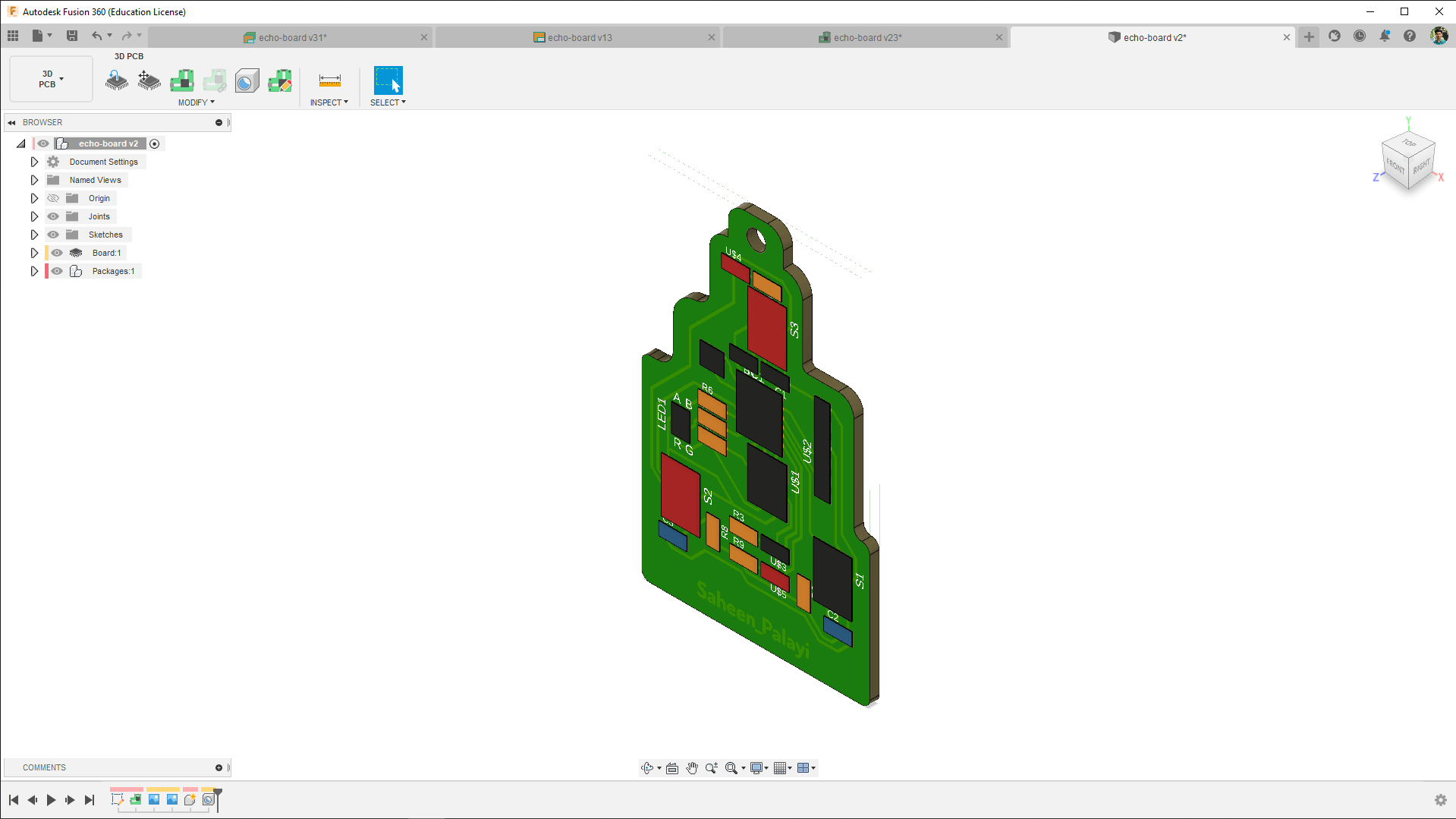
So after a some lags a new opened with a 3D design of my Badge PCB with dummy components.I found out the library I'm using don't have 3D version that's why I don't see any components in it
Here is the picture of my PCB without the packages which actually looks great.I do want this 3D model to complete by adding 3 d packages of components so I learned to edit the library.
Milling ..
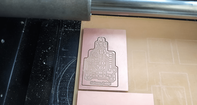
So the both files for Milling process is ready.I loaded a new PCB on Modalla MDX-20 milling machine and opened the 'traces.png' file in the FAB MODS.
Then followed the procedures like I did in the Electronics production week. calculated the tool paths and set to the machine.
After the traces are milled out I sent the outer cut file ("cut.png" ) for cutting out the PCB we can see al the milling process in the above time laps video clip.
During the outline milling I noticed the hole in the PCB milled out after the outer line that occurs a misalignments in the position of hole. We can see that in the above picture. To avoid the problem I should mill the hole first then the outline but the FAB MODS creating the tool path as the outline milling first.

So I opened the 'cut.png' file to the GIMP again and removed the outline profile then saved as 'drill.png'

And again saved another copy for outline but this time I removed the hole from the file. this is not necessary any more I already fabricated the PCB and the misalignments is not a big thing for this assignment.Now I understand what other things to take care while milling
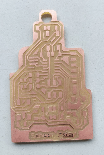
I taken out the PCB from the Machine and cleaned ,Inspected to make sure I got all traces without any short .I know it's not symmetrical but It look beautiful.
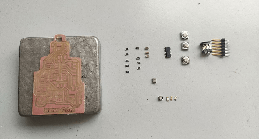
Preparing Components
So the PCB is ready for soldering required to collect all the necessary components from the lab . The components that I'm collected is given below
Unfortunately our LAB ran out the Attiny44 microcontroller but I got Attiny84 instead both pins and features are same except the flash memory size its twice than the Attiny44.But that's a good thing
Then I prepared all the components on soldering work bench and pealed all the component's covers to start soldering ..
Soldering
Then I started Soldering staring with smaller components like Resisters capacitors..... see the time laps below
soldering the smds not a big thing we done already during electronics production but soldering the crystal was different we can see the time laps first I tinned both the pCB's and crystal's PAD then placed in position with flex and then heated up to make solder in position
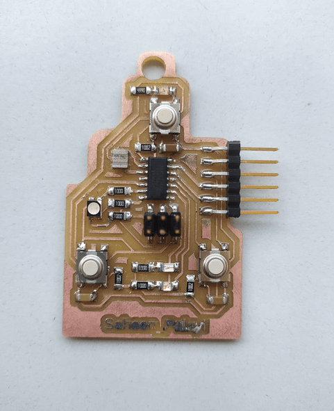
So the Production is complete.All inspected no shorts ready to test. Finally made what I designed !! .
Programing
For testing the whole board is working or not I Programed a basic LED blink sketch in my echo_hello_world board with the help of Arduino IDE.It is open source so the arduino ide working with the avr tool called avr dude. so it supports all kind of AVR chip.visit arduino.cc for more
I already have arduino in my windows pc for fab I did it linux.I downloaded the 64 bit installation file
After downloading file I extracted and installed in ubuntu by following the tutorial provided by arduino.cc
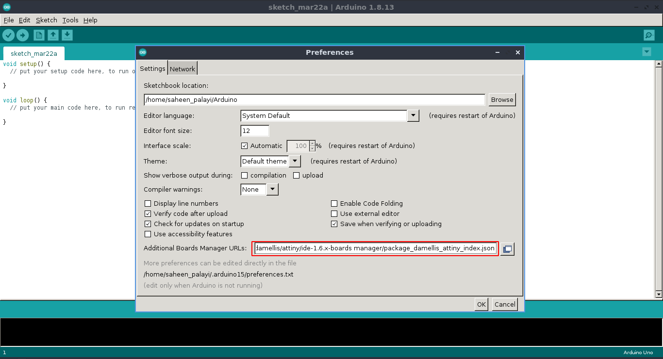
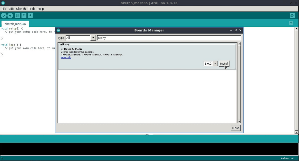
https://raw.githubusercontent.com/damellis/attiny/ide-1.6.x-boards-manager/package_damellis_attiny_index.jsonThen added the above Link in file>>preferences .This link contain the attiny24/44/84 packages then click oK
Then open arduino Boards Manager by following Tools>>Board>>Boards Manager Then type Attiny it shows a package and clicked install
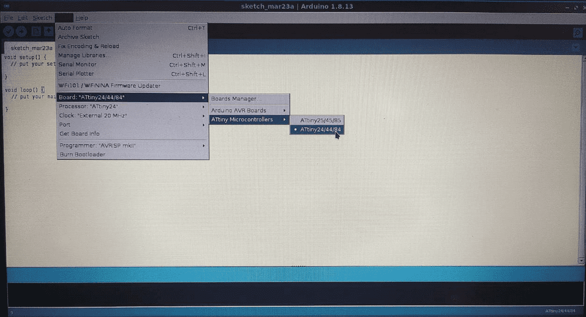
Now you can see new boards are added in the boards menu, selected the Attiny microcontrollers>>Attiny24/44/84
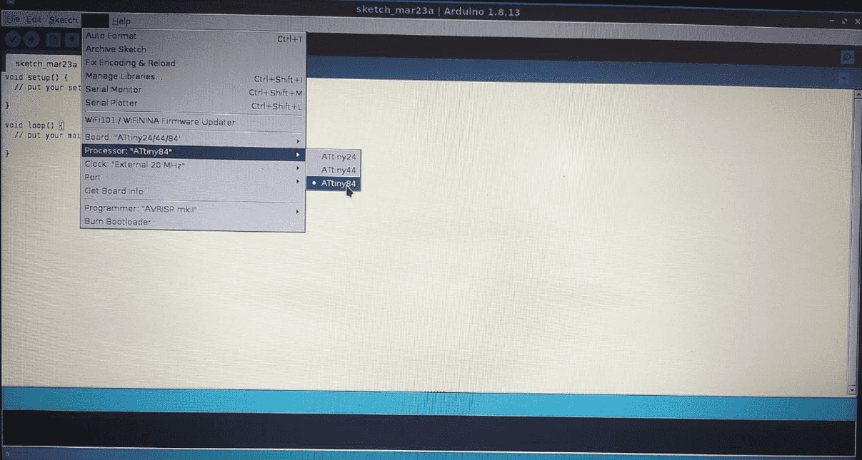
then I selected the processor as Attiny84
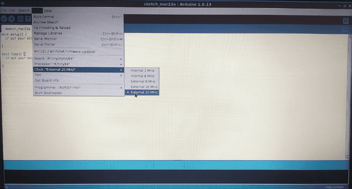
Now I have to select the Clock type ,I have a external 20Mhz resonator on-board so I selected External 20Mhz
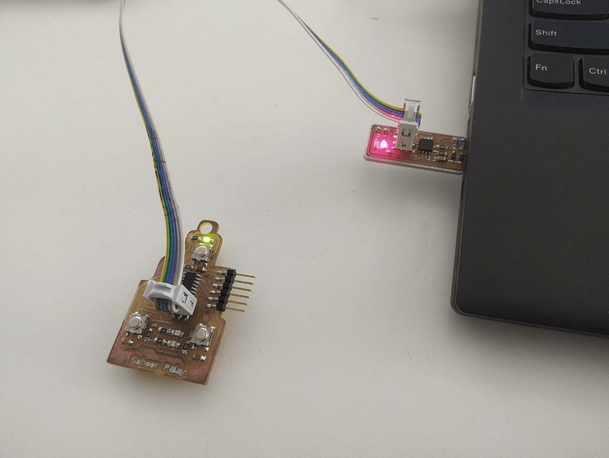
next i selected the programer .the programer I'm using is the FABtiny ISP or USBtiny ISP whcih I made during Electronics production week
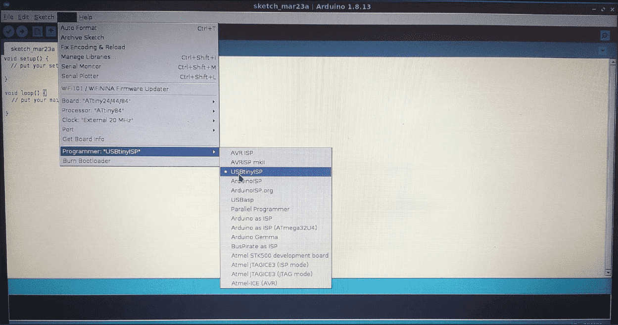
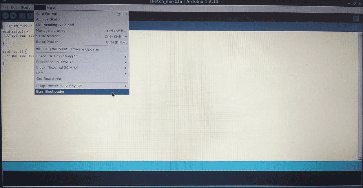
all the board configurations are set now we have burn the boot loader that include the instructions for microcontroller like using external clock or internal.I plugged the board with ISP programer to pc
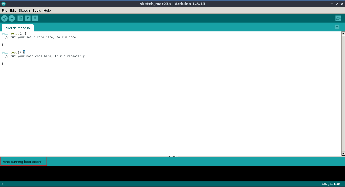
Then I clicked burn boot-loader folowing Tools>>Burn Boot-loader
If Everything is the arduino IDE will show Done Boot-loader.Mine was perfect!
Then I opened a very basic test program on arduino called Blink ,For Blinking the LED following File>>Examples>>Basics>>Blink
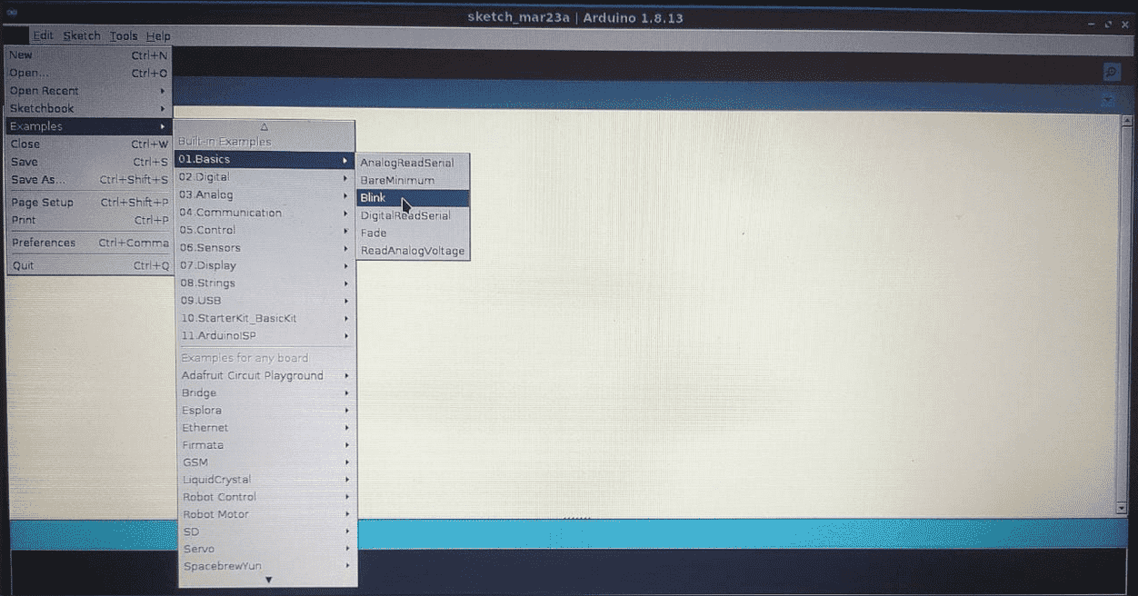
That opens a program with new window .Then I changed the 'LED_BUILTIN' replace with My LED PIN
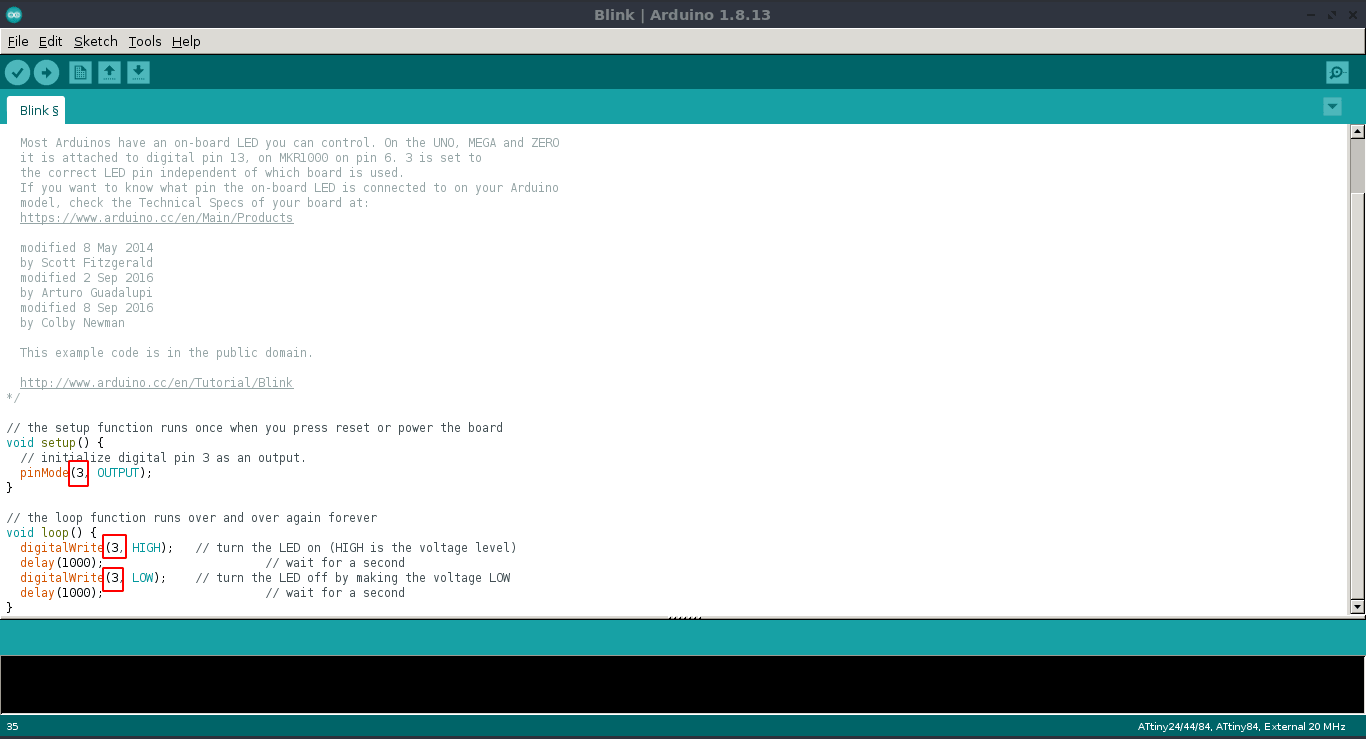
one of my LED is PA3 whcih connected to Ic's 10th PIN for arduino its Pin '3'
I found the PIN number from above diagram.Then I uploaded the blink program to my board.
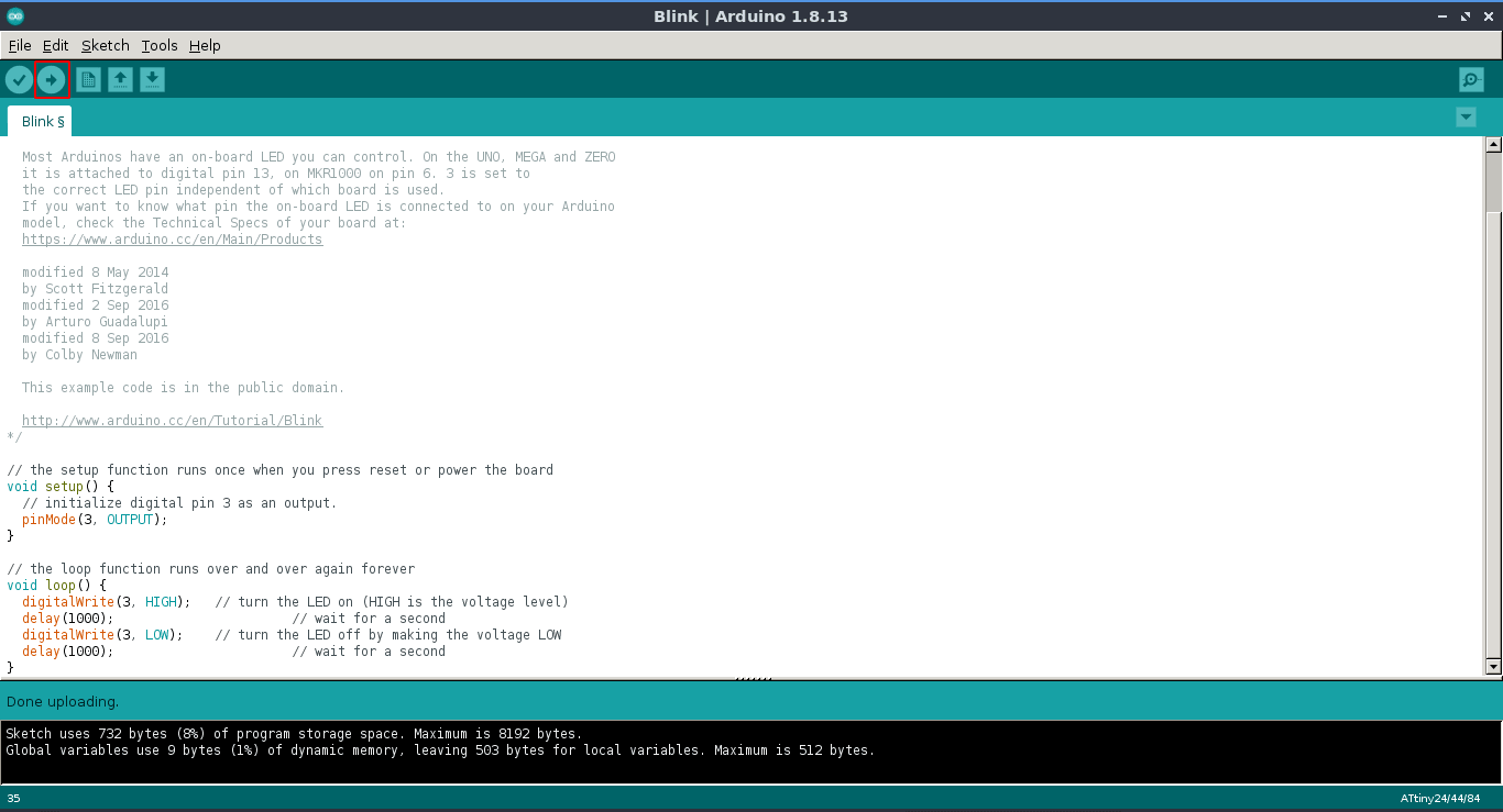
My blue LED starting blinking with 1 second time intervale.
Programing with AVR Dude
In the echo hello world examples shows in the academy website also given sample programs. I'm already programed my ISP using AVR dude so I decided to program a given c program to my board to see its work using avr dude.
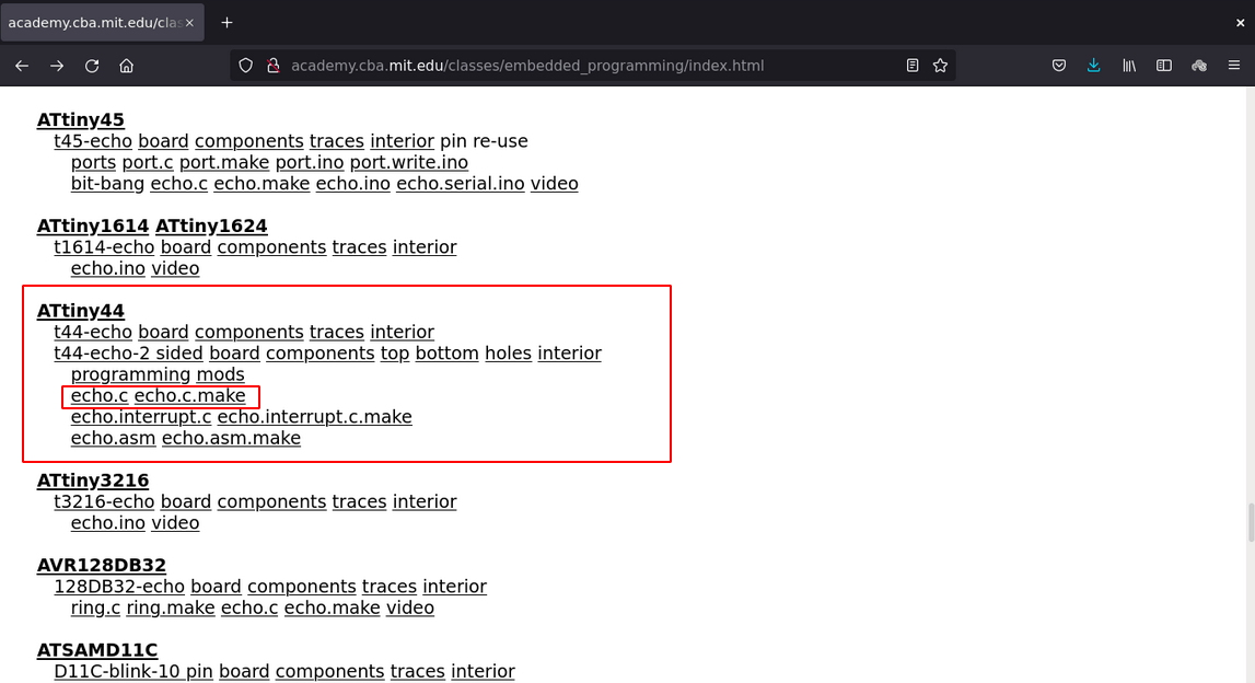
FIrstly I download these 'echo.c' and 'echo.c.make' files from the academy's Embedded system classes page.
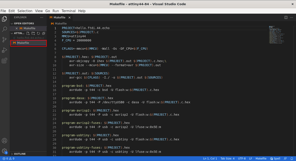
Then moved both file into a folder and opened in visual studio code then renamed the 'echo.c.make' to 'Makefile' .
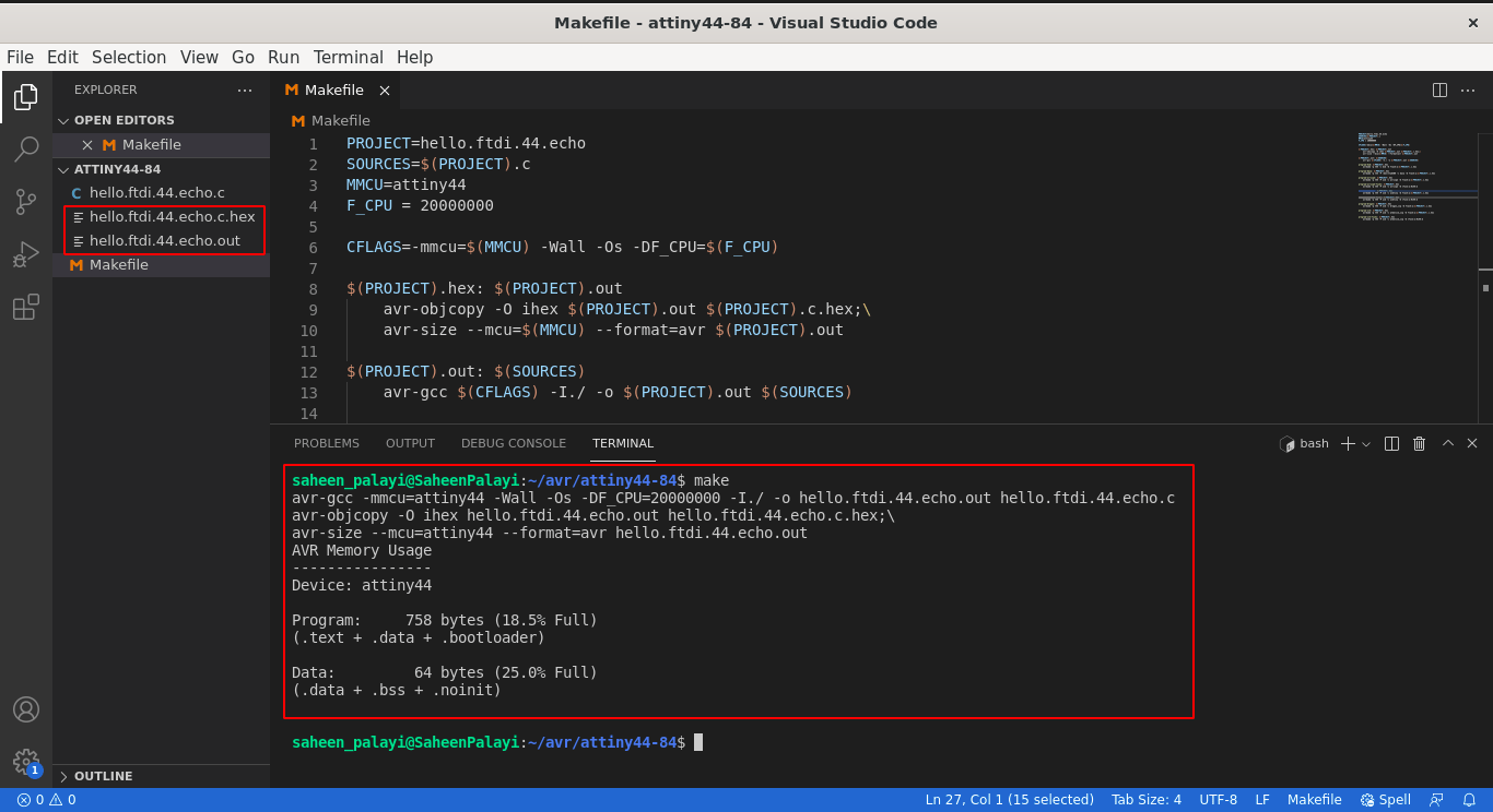
Then in the vs code terminal I entered 'make' that created the .out and .hef files to program from the source file echo.c .
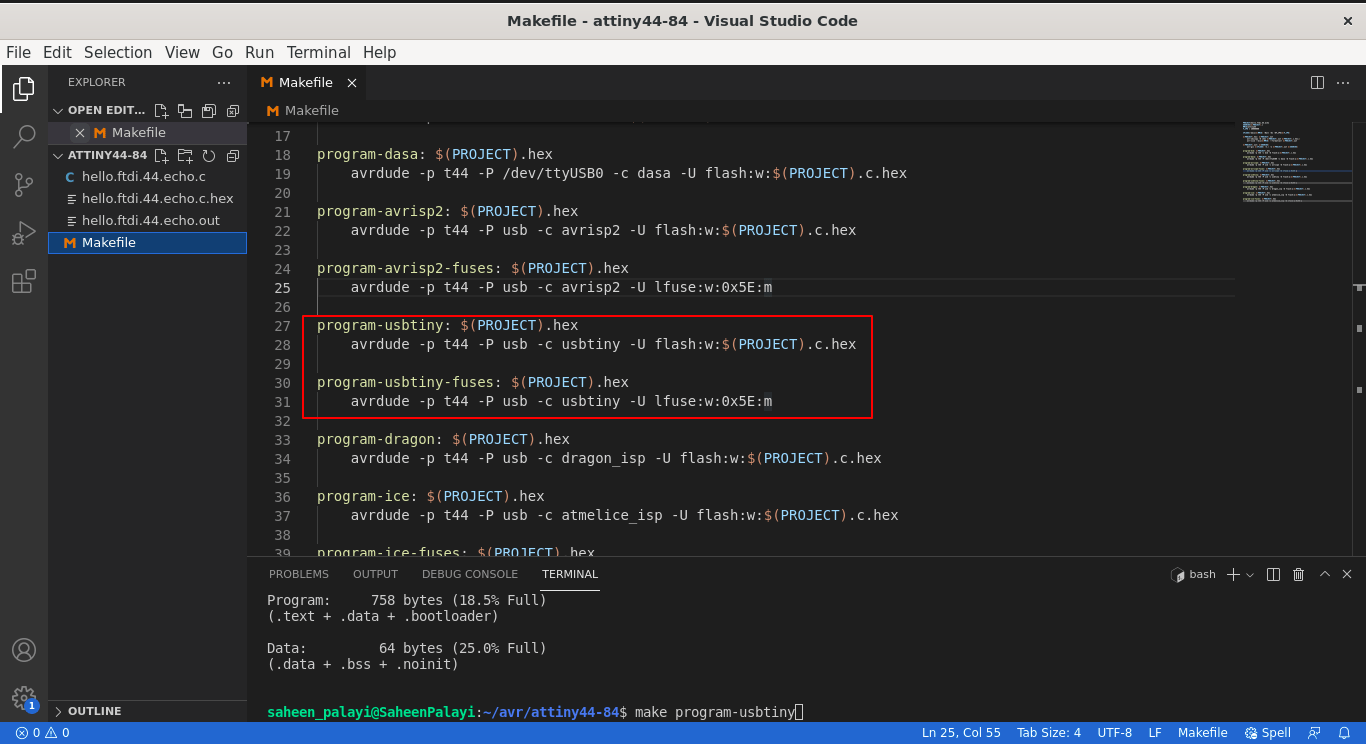
In te make file there are many codes already set for programing with different programer.I found the codes for the FABtiny ISP we just need to type them with the make command in the terminal after plugging the ISP and attiny44 echo hello hello-world board.
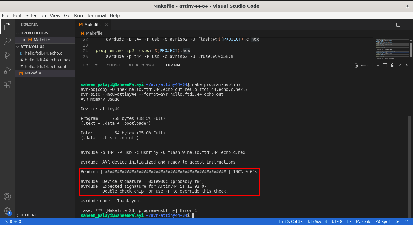
Then I plugged the board andy enter the command 'make program-usbtiny' in the terminal , Then its shows an error reading the chip because its not attiny44 that I'm using so I have to change to attiny84 in the make file.
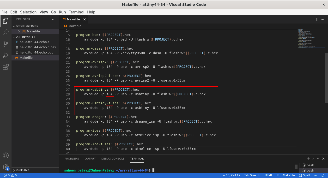
So I renamed all the code segment which is labeled 't44' in the make file to 't84' and run the programing again...
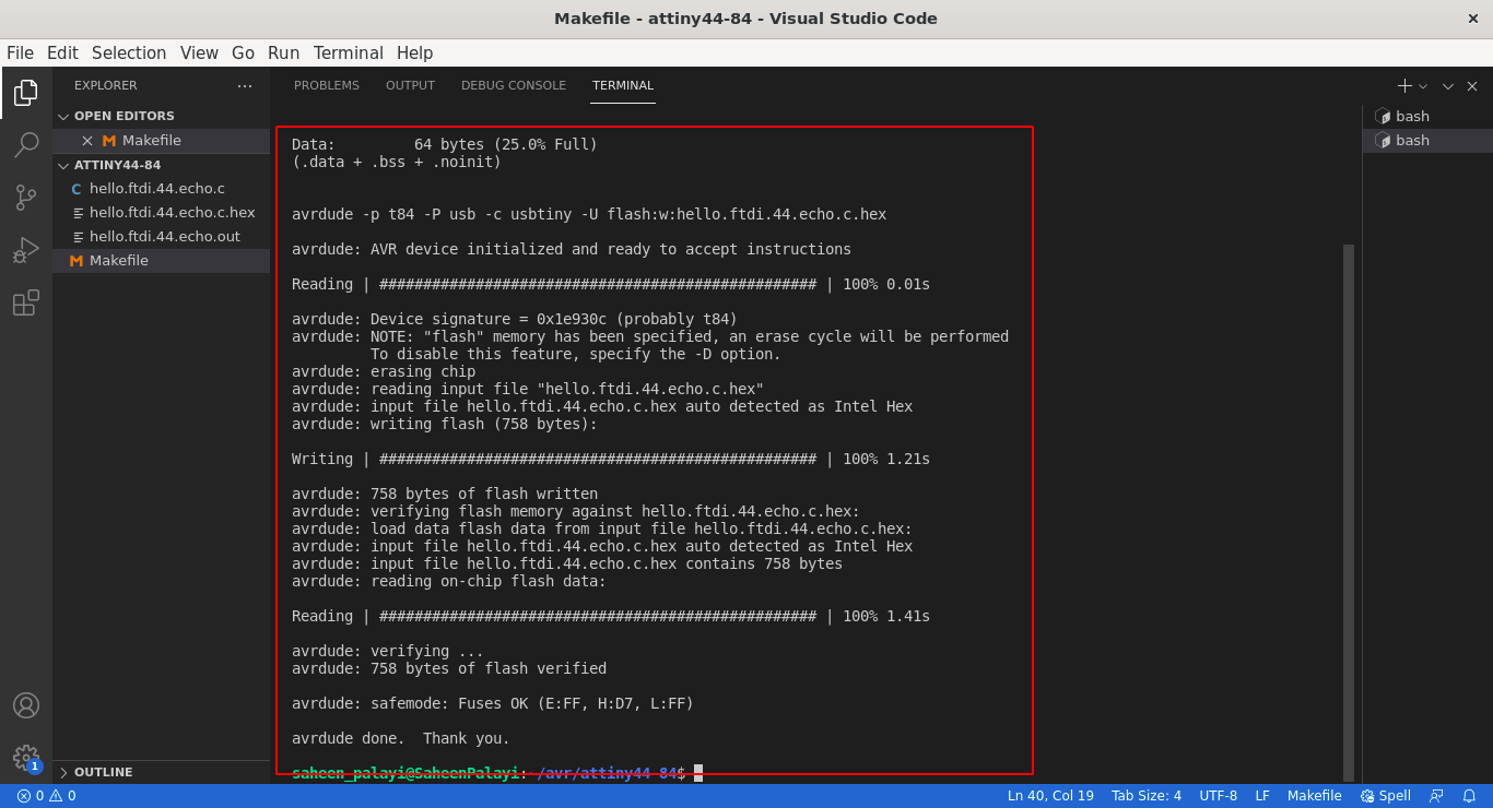
Yes!. this time it is programed the attiny84 chip with the 'echo.c' program.So basically yhe program works through the serial RX,TX protocol called UART (Universal Asynchronous Receiver/Transmitter).In order to do that we need to connect to an arduino Serial Monitor in the computer or any other UART serial Program.
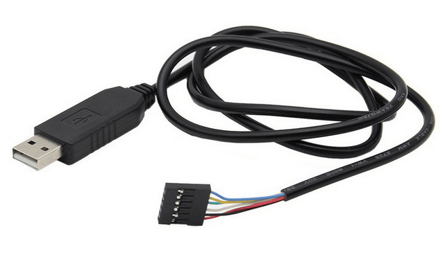
Todays computer doesn't have any Serial ports to talk with UART devices so we need An USB to Serial Converter. Its called FTDI Converter(FTDI is an company name who makes the chips and converters).In our lab we have FTDI cable like in the above figure, It has an USB connecter at an end and another end 6 Pin Female header with colour coded for the serial communication.
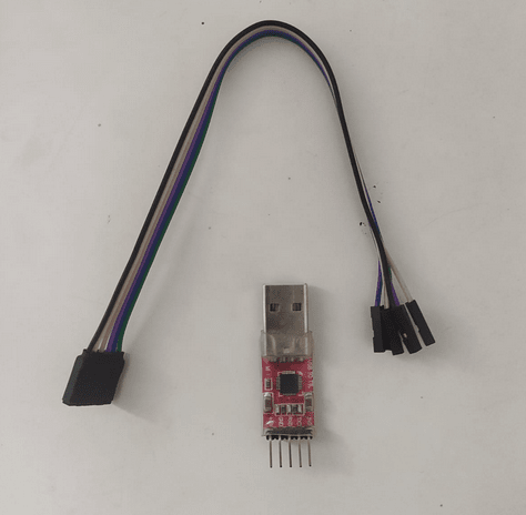
The cable was busy in the lab because we only have one or two so I Had a an CP2102 USB 2.0 to TTL UART Serial Conversion module.This thing also work and it doesn't have all the pins like CTS,RTS. And that's not needed at all.
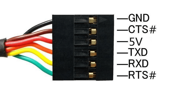
The above picture shows the Pin outs of the FTDI cable. We dont need the # tagged pins which are CTS and RTS for the Serial Communication.
So using the Female to Female jumper wires I managed to connect the Serial Converter and My Board like in the above figure.
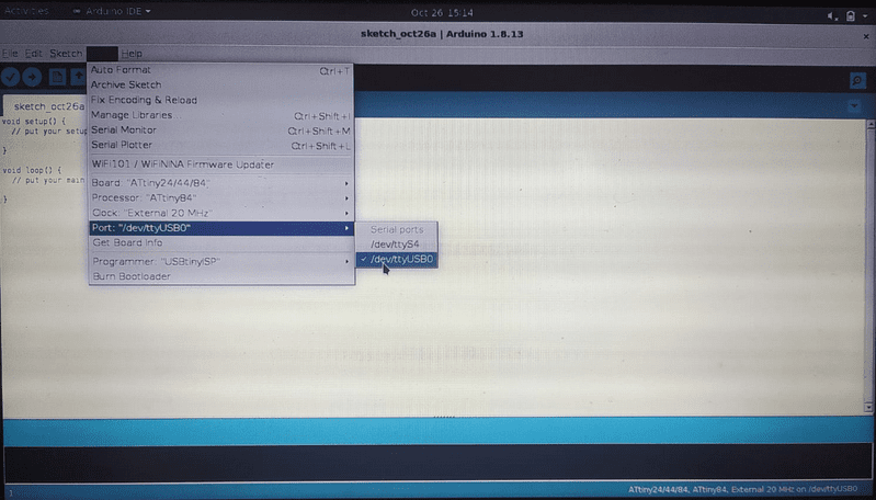
In order to communicate with the board we need a software program called 'Serial Monitor',So for that Opened Arduino IDE and selected the Port for the Serial Interface
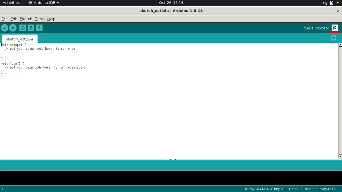
The Serial Monitor program is Built in the Arduino IDE we can find it in the tools or click right top corner 'magnifier' symboled Button as shown as above. So I clicked on it.
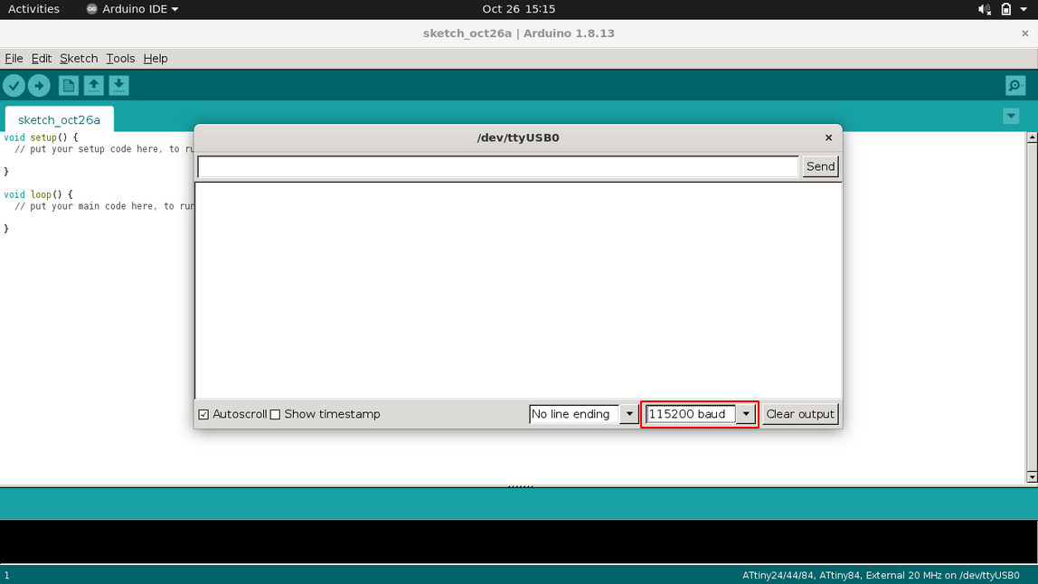
Then The Serial monitor Opens Next we need to set the Baud rate That is already mentioned in the Echo echo_hello_world Program which is '115200' . So I set the baud rate to '115200' like in the picture.
In the serial monitor I typed "Hello World" by each characters like shows in the above screen record video. Each time the Board Echoes with the characters which I typed previously typed. I can't type all the words in one go because the program only red,store and echoes single characters. So that's How the program works we are gonna explore more in the upcoming Embedded Programing week.
Hardware Simulation
Doing circuits always by connecting components together or doing productions directly is a costly process and need lot of money and effort to get the results. So we have to make sure The circuits and components are right for production or fabrication. For that we relay on Simulation softwares or Spice simulators,These softwares have all the basic components and some even have microcontrollers for Hardware simulations. Each components are a pice program according tot their working and predicted outputs.
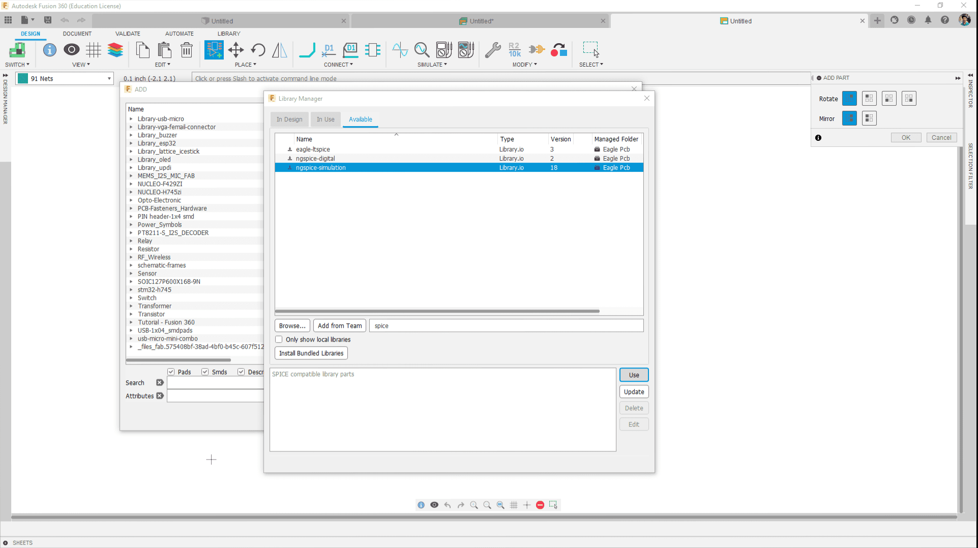
In Fusion 360's Electronics cad already support a spice simulation feature which we can do with the help of a library provided by Autodesk Fusion 360. Here in the above screen shot shows which one I installed. I was following this Youtube tutorial from a guy named "Dan Puperi".
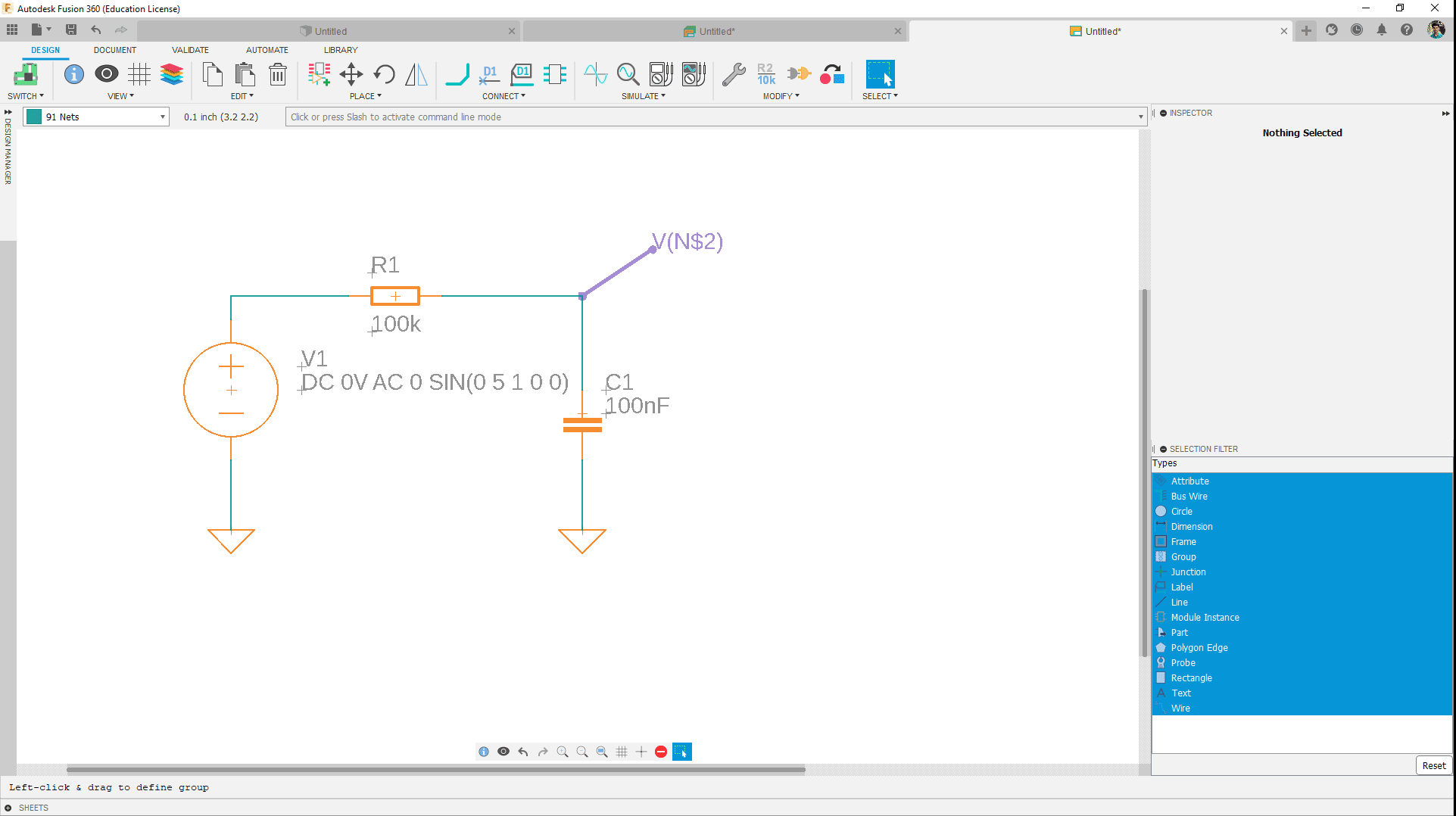
I simply made a Low Pass Filter Circuit with using a resister and capacitor following the above mentioned tutorial.
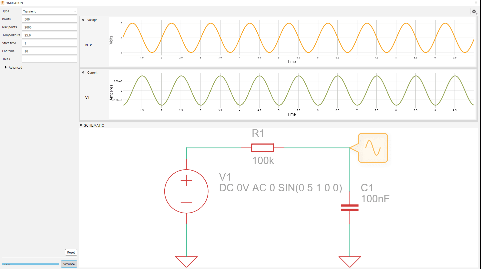
This is the result which I got in the Low Pass Filter circuit as Input and Output simulated Oscilloscope wave graph with respect to the time.
For about the Fusion 360 electronics cad spice simulation follow this Webinar tutorial from Autodesk Fusion 360.
Simulating with Thinker CAD
Thinker cad is an educational platform especially for kids which is not required any installation we can just use in our Browser.In Thinker cad we can do Electronics simulation platform which is based on AVR/ARDUINO environment.
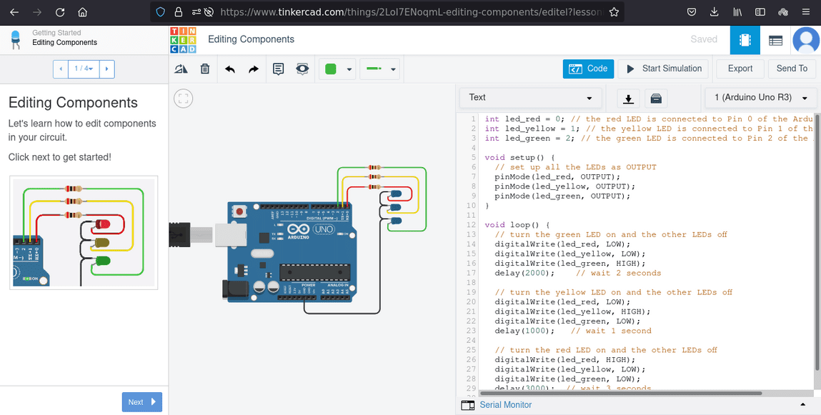
The above figure shows a learning example that we can find in the Thinker cad circuit simulation which is do 3 LED chasing effect. in the Right window we can see the code and also possible to modify and build the Code our own.
This video shows how we run the simulation in Thinker cad. we can see the blue LEDs are start ON/OFF one by one after I clicked the start simulation button.For more checkout Circuit Designs in Thinkercad
Attiny84 Badge Simulation in Proteus
Proteus Design suit is one of the professional design studio for Electronics and Embedded Engineering . I get know about this software program while I'm studying Engineering ,It's an all in one software where we can draw schematic , PCB design, and especially Realtime Microcontroller Circuit Simulation. It supports vast verities of microcontroller like Avr ,PIC ,arduino etc...

What I have is an older version of Proteus studio which is Proteus 7 got from my Technical College for studying embedded simulations.It's actually a paid software, the one I have was bought by my college for educational purposes. For more please visit labcenter.com.
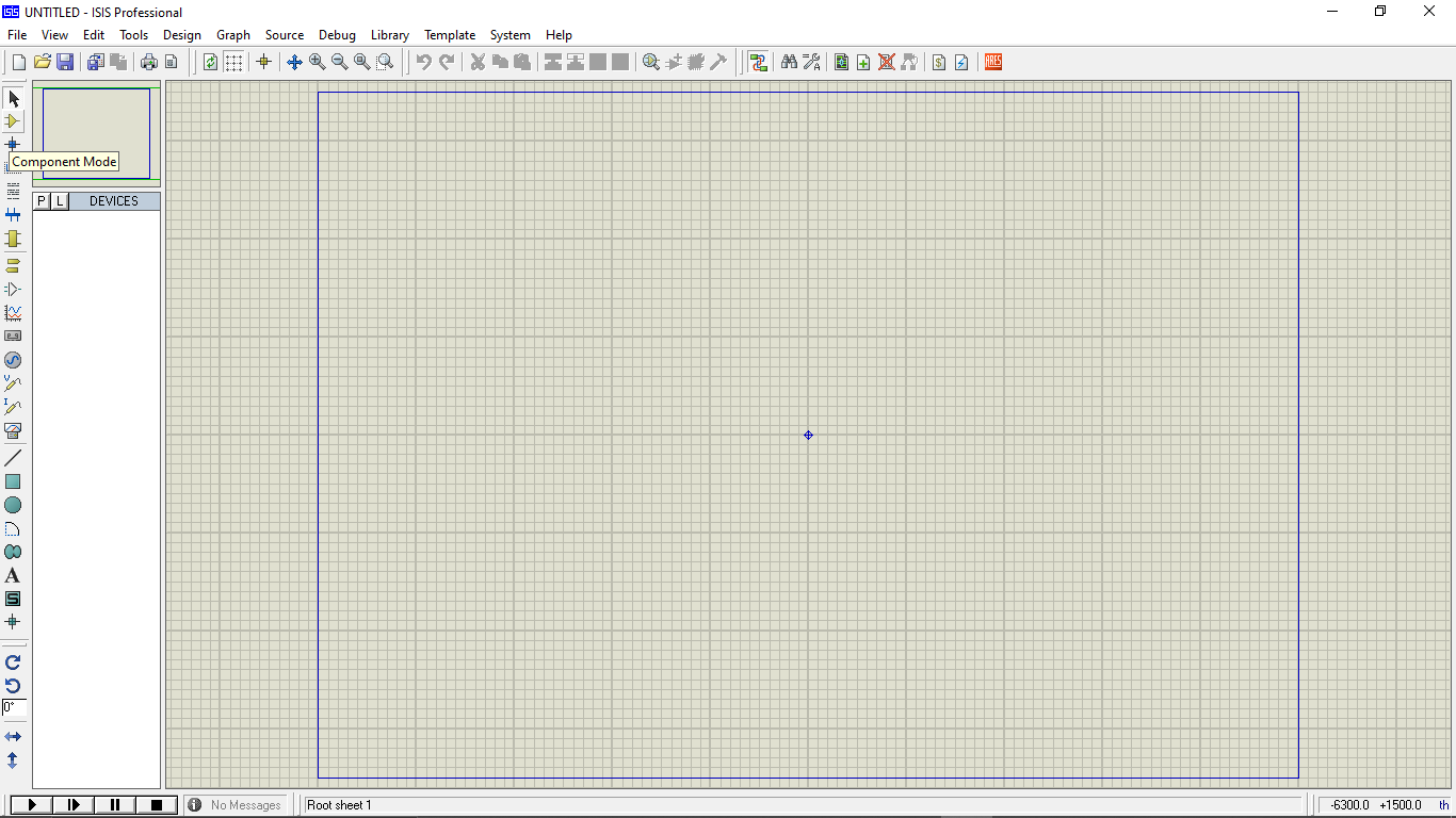
FIrstly I opened the ISIS Proteus Design Suit and clicked on Component mode from left side bar to start drawing the Circuit
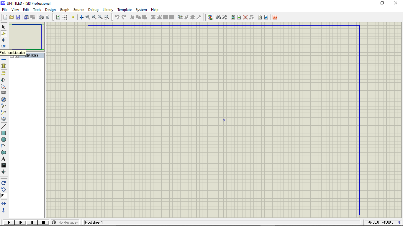
Then on the following side window pressed P to pick components from the proteus library.
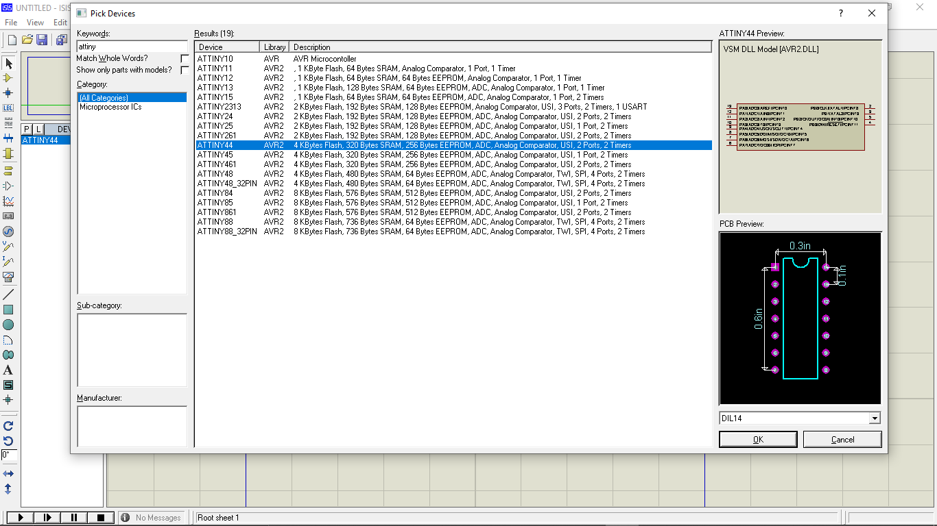
The library window popped up as next step there are many components available for circuit simulations. So I found the Attiny44 from the Microcontrollers category.
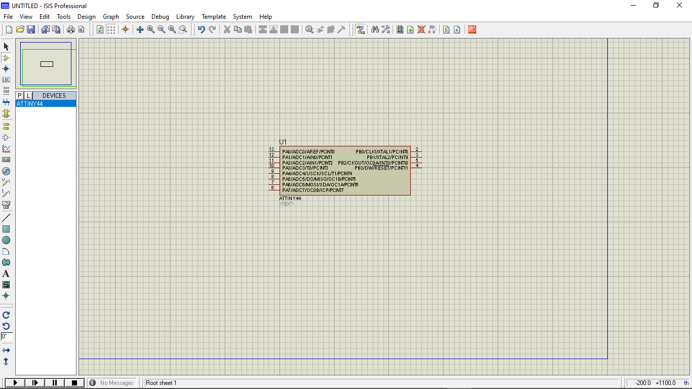
And Then I placed on the drawing environment at the center ,Then I started to add rest of the components I need for simulation as in the Electronics badge's circuit I made this week.
Now the Circuit all set for simulation but Missing the programing part to the Attiny44. So we can directly add the corresponding hex code to the Simulation Circuit for running the simulation.
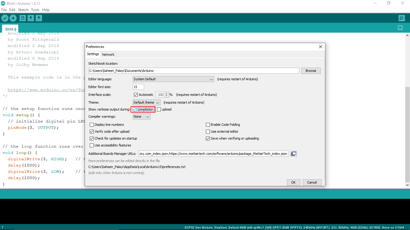
For the simulation we need hex code file of the program that we are gonna run to the attiny-44.So, In arduino we can locate the hex code file of the program which generated while compiling process to locate that I Enabled the 'Show verbs output during: Compilation' option for knowing the path like in the above screen shot.
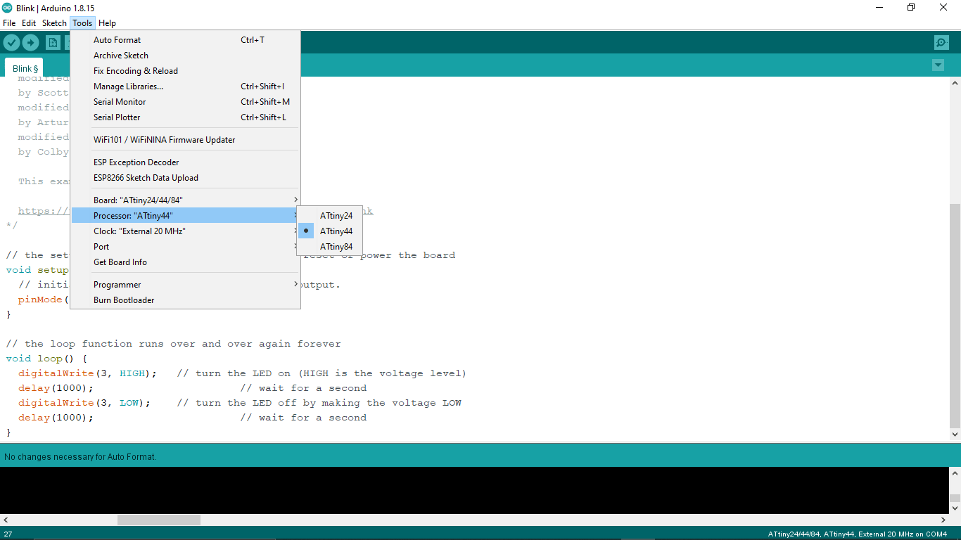
Then I selected the microcontroller board as 'Attiny44' and the clock as 20Mhz in the Tools Then I opened the same program which I used for blink led test in my echo hello world Badge PCB.
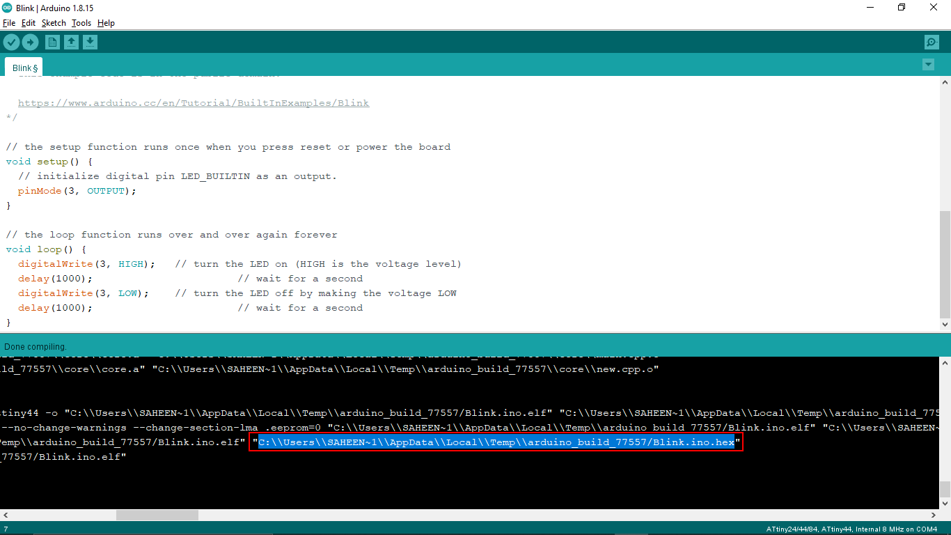
The path name for the hex code will show up in the status terminal below I selected and copied the path name from there.
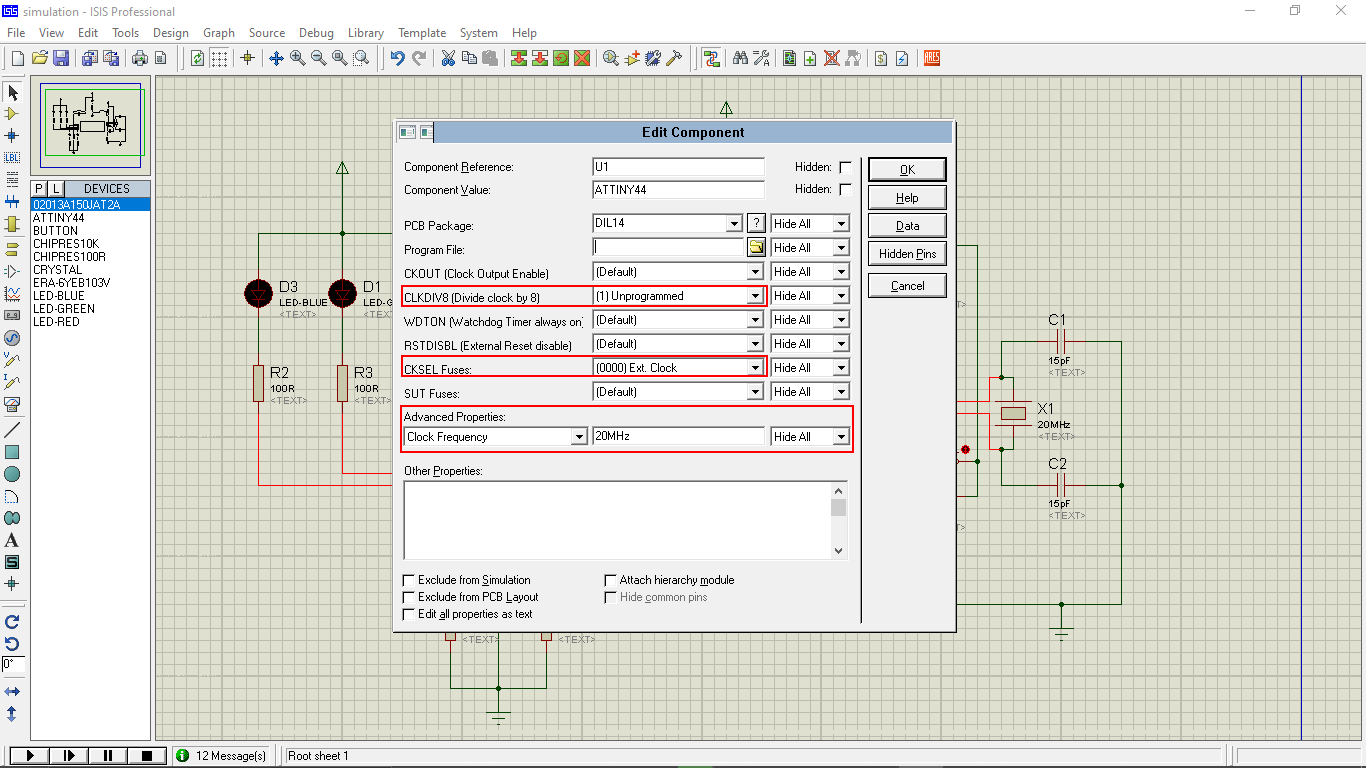
In proteus if we click on the microcontroller we can set the clock fuses and crystal frequency, program paths . SO I double clicked on it and set the clock and clock div fuses and also the clock frequency like in the above figure.
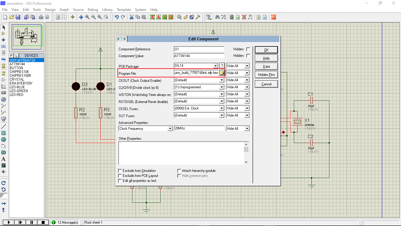
Then I pasted the 'blink.ino.hex' file path name in the window for attaching the compiled program to the simulator. And clicked 'Ok'.
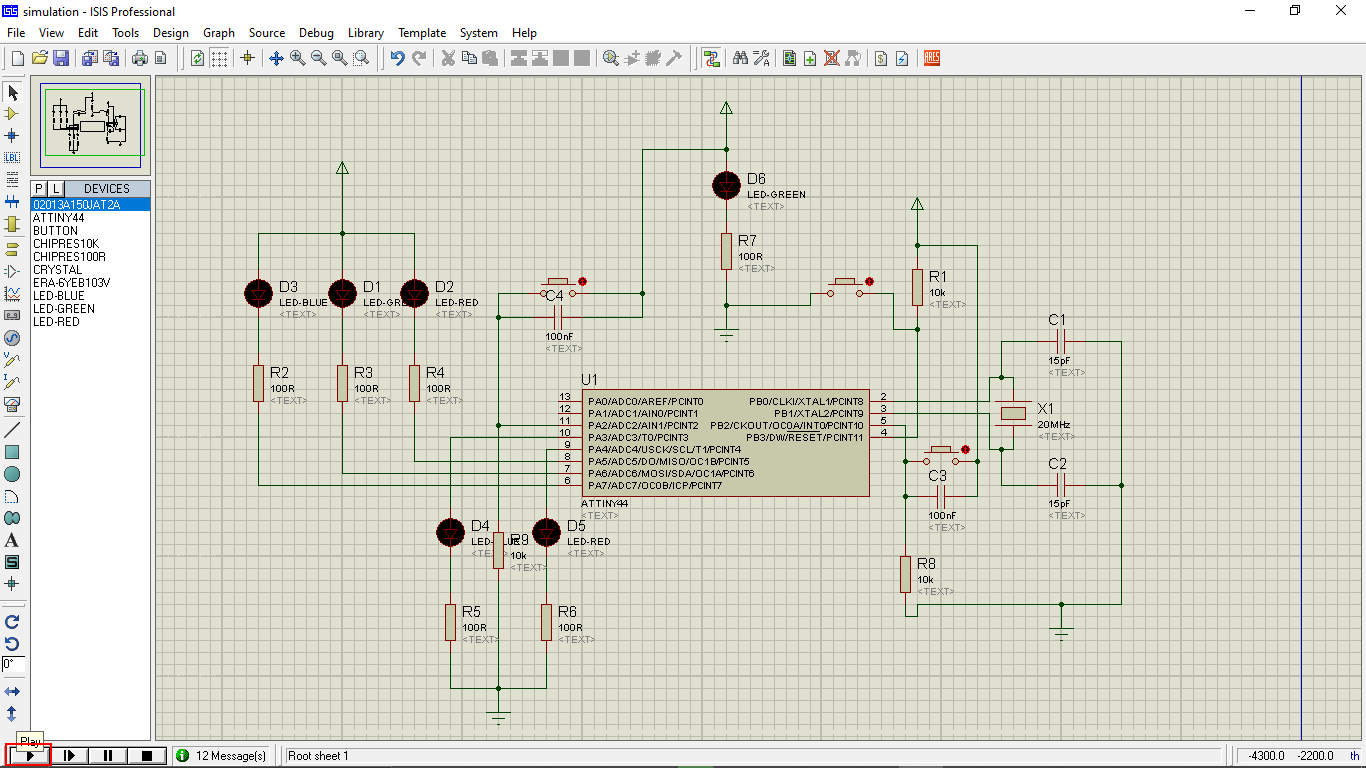
Now I have to run the simulation by clicking the play button from the bottom left simulation controls button section.
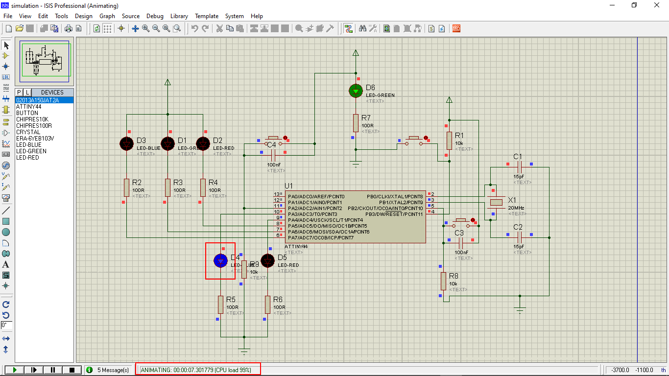
We can see the blue LED starts to glow periodically with 1 second time difference the clock running by the microcontroller can be seen in the bottom left , which helps to identify wether the LED is is blinking with accurate delay or not. And also the Green Power LED turned on While the simulation running.
Here is the screen record video clip of the proteus simulation of my echo hello world badge circuit. We can also stop the simulation also can run after editing the program in the Arduino IDE. we already given the hex code file location so in the next time when we compile the hex code will update and it's more like play and pause system.It's awesome!
References
- Fabacademy Electronics Design classes
- Fabacademy Embedded Programming classes
- www.elprocus.com | Elctronics Tutorials
- www.codrey.com | Elctronics Tutorials
- www.theengineeringprojects.com | Elctronics Tutorials
- www.watelectronics.com | Elctronics Tutorials
- www.tutorialspoint.com | Elctronics Tutorials
- components101.com | Elctronics Tutorials
- www.toppr.com | Elctronics Tutorials
- top10pcb.com | Elctronics Tutorials
- www.delabs.net | Elctronics Tutorials
- circuitdigest.com | Elctronics Tutorials
- in.element14.com | Bench Power Supply
- www.electronics-notes.com | Elctronics Tutorials
- www.oreilly.com | Arduino Tutorials
- Blink | Arduino
- EasyEDA CAD
- Autodesk Eagle CAD
- Autodesk Fusion 360
- Fabacademy Tutorials Eagle resources
Downloads
- PCB Design Files
- Circuit Simulation Files