Use the test equipment in your lab to observe the operation of a microcontroller circuit board (in minimum, check operating voltage on the board with multimeter or voltmeter and use oscilloscope to check noise of operating voltage and interpret a data signal)
document your work (in a group or individually)
Select and use software for circuit board design
Demonstrate workflows used in circuit board design
For this task I used the fab academy reference to create the Atiny44 circuit board.
Since we used eagle on the previous winter camp, it was my preferred tool to create the circuit. After installing eagle, I also had to install the Eagle fab library to ensure that I was using components with modified sizes that relay maximum efficiency when designing the board.
To start using the fab library, I had to physically copy the file into the eagle lib directory.
Then I created a new project in eagle and started working in the schematic window. I clicked on the add part icon on the left hand tool bar to access the library and navigate to the fab library named eagle_fab in my laptop.
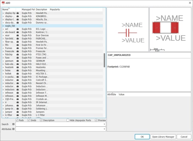
Then I looked for each component, and added them to my schematic. Since we were required to add at least one input and one output to our circuit, I decided to add an ;LED along with a button. The components I used are listed below:
| Quantity | Component |
|---|---|
| 1 | Atiny 44 14 pin microcontroller. |
| 1 | XTAL Resonator. |
| 1 | 10 Kilo Ohm resistor. |
| 1 | 1 micro-farads Capacitor. |
| 1 | 3x2 AVRISP SMD connector. |
| 1 | 6 pin header. |
| 1 | 499 Ohm Resistors. |
| 1 | 6 MM Switch. |
To calculate the resistor value for the LED used (Yellow SMD 1206 LED), I checked the datasheet for the forward current and voltage.
Then using A simple equation (source volatge - forward voltage)/(forward current) we can determine the value of resistor needed.
In my case (5-2.5)/0.02 which would equal 125 Ohms. That is the minimal resistor value that can be used for the LED, however, in our lab, the least value of resistor availabe was 499, thus I used the later value.
I placed the components just as Our instructor Hashim taught us with the connector having its VCC side on the right and the GND on the Left and used tags to connect the components together instead of using direct links, hence it would be easier to modify later, and much more comfortable on the eye.

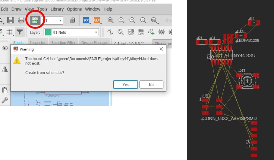
After ensuring that the components are connected directly, I converted the schematic diagram to a Board diagram using the switch/generate board tool on the top tool bar.
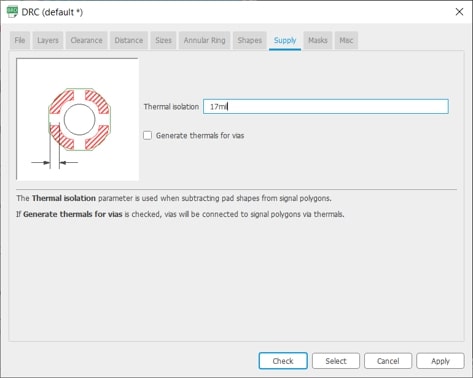
I moved the components to the workspace first , and then clicked on the DRC icon on the left tool bar. This tool is the design rule check, and it checks the design and routing based on the values fed in by the user.
This step is crucial to ensure that we are applying enough constraint on the design so the milling bit would engrave the traces and pads of the components correctly ensuring that the design would function properly and reliably.
In this window, I changed all the values under clearance to 17 mil and changed the minimum width under Size to 17 mil as well.
![]()
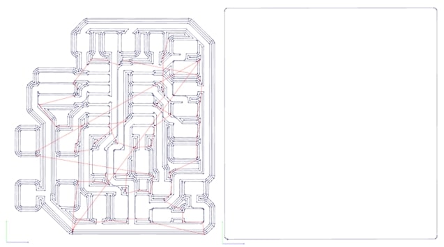
I used the routing tool on the left toolbar to connect the traces between the components. Most of the components were easy to connect, however, when it came to the ground and VCC, some connections kept clashing or crossing.
I changed the placement of the components, changed the tags in schematic and redid the routing, tried squinting and looking hard at the board to look for a solution (which needless to say, didn’t work at all).
Eventually, it got quite frustrating that I kept postponing this task .. not the best idea =(
Then later after consulting Hashim who told me that I can change the wire width to 12 instead, I was finally able to connect all the components together.
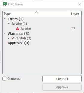
I re-clicked on the DRC icon to check for any errors, and man I had some! I had an air-wire hanging and some wire stubs. Fixed that quickly by re-routing and removing the stubs and were good to go!
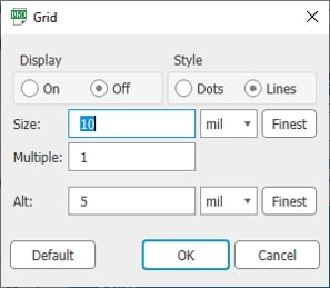
I also opted for changing the resolution by going to the Grid icon in the upper left tool bar and change the default value 50 to 10 which permitted smoother routing.
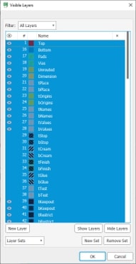
Before exporting my image, I had to hide all the layers except the red layer that shows my connections, that is done by clicking on the layers icon on the upper toolbar, hiding all the layers and showing only the red.
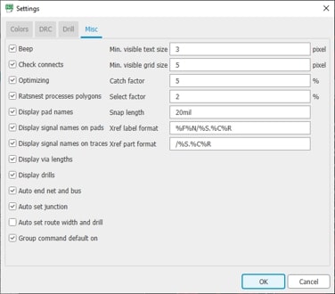
Now that leaves me with the labels that I also want to hide by going to options tab >> set >> and MISC >> de-check everything that has display
Finally my board diagram looked like this!

To export my board as an image by going to file >> export >> image, and change the image characteristics. I chose the maximum resolution value 2000 dpi and checking the monochrome box.

The pictures are then saved in the directory of my choice in PNG format.
I used paint editor to edit the traces image and create the outlines by simply Covering the traces with a white filled BOX.

Then I used the fab modules to create the .rml format for my traces and outlines. The exact steps for the process can be found on my electronics production page.
while performing this step, I found out that the parameters of the picture was suspiciously too large, in fact it was double the size of the board I had on eagle!
This was due to the fact that I had my laptop display settings to 150 % when exporting my image, which resulted in deformed parameters.
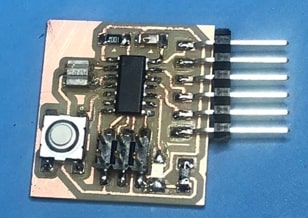
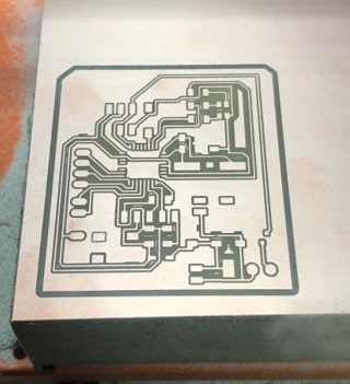
Then I used the milling machine to engrave my traces, and I soldered the components. The exact steps to do so are in the electronics production page.
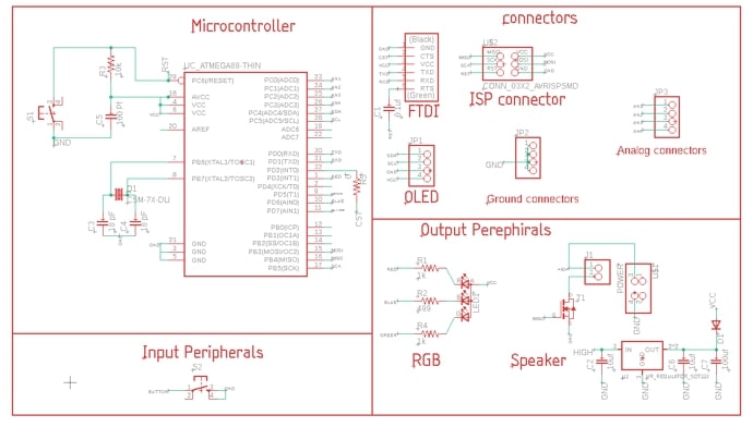
My extra work this week was to redesign a basic hello.328p board, I used the board Niel created and added inputs and outputs that would resemble the operation of my final project board.
For this task, I also used Eagle, hence it is the software that I am most confident with.
The list of components I used on this board are the following:
| Quantity | Component |
|---|---|
| 1 | Atmega 328P/88A 8-bit AVR micro-controller. |
| 1 | 16 MHz Crystal Resonator. |
| 1 | 10 Kilo Ohm resistor. |
| 2 | SMD push buttons. |
| 1 | 100 PF capacitor. |
| 2 | 22 (or 18) PF capacitors. |
| 1 | 0.1 uF capacitor. |
| 2 | 10 uF capacitors. |
| 1 | 100 uF capacitor. |
| 1 | 10 K-Ohm resistor |
| 1 | 0 Ohm resistor. |
| 2 | 1 K-Ohm resistor. |
| 1 | 499 Ohm resistor. |
| 1 | RGB LED. |
| 1 | Mosfet transistor type N. |
| 1 | Diode. |
| 1 | FTDI connector (1x6) |
| 1 | ISP connector (2x3) |
| 3 | Through hole connector (1x4) |
| 1 | Terminal (1x2) |
| 1 | Power jug connector (2x2) |
| 1 | Speaker. |
| 1 | OLED screen. |
For this board, I tried using outputs that I might use in my final project. To understand the connections of the board, I used the input devices and output devices week pages references.
The process of creating this board took a lot of time. The mere process of thinking and researching about the modules that could be added was time consuming, but it was definitely worth it as I learned a lot.
Hence, my schematic:
As usual, routing took the best chunk of time. This time instead of connecting all the GND points, I created a “common ground” by selecting the polygon on the left tool bar, selecting the area around my components and clicking on Ratsnets.
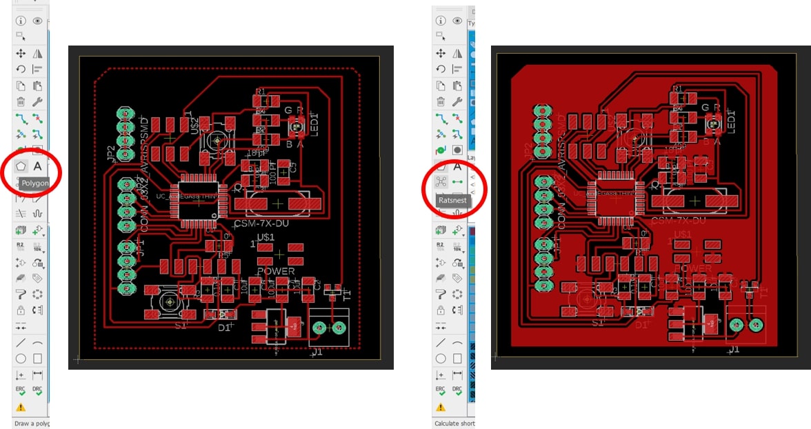
My final board diagram:
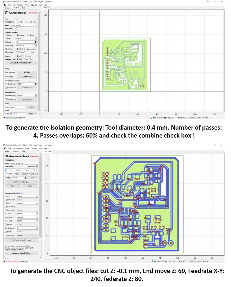
This time instead of using fab modules, or mods, I used a software called FlatCam which is an open source program that prepares CNC jobs to create a PCB on a CNC router. It basically takes the Gerber files generated by the PCB cad program and creates a G-code for the isolation routing.
The reason why I am currently preferring FlatCam over other tools available is the ease of transition and conversion of the files; a simple modification on eagle for example would be followed be several other steps when using the other tools, but the transition is quite easy with flatcam as I only need to export the files once only.
To export to flatcam, I use the manufacturing tool on the right side of the board diagram page, and launch cam to open the cam processor, generate and export the Gerber files.

Then I lauch flatcam and open the Gerber files (for the traces and the outlines) and the Excellon files (for the drill parts) required, and enter the values accordingly.

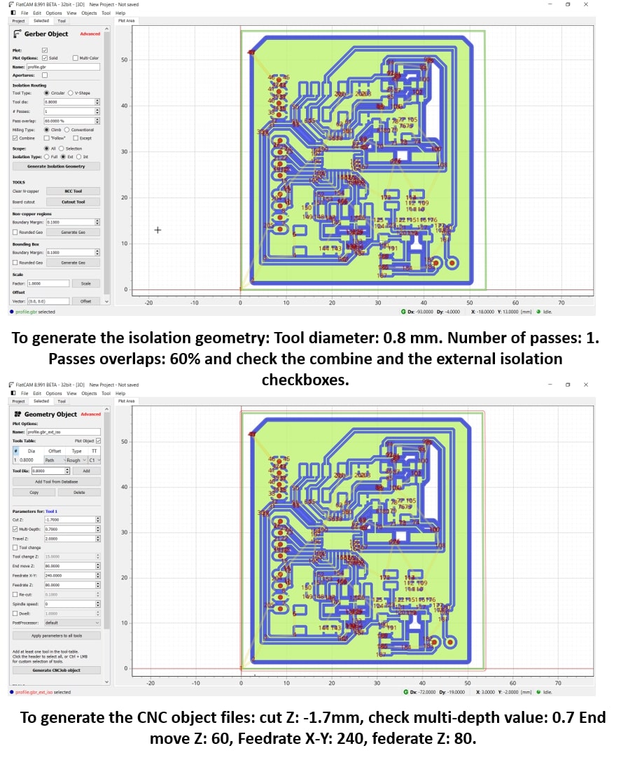

I used the Roland SRM-20 CNC machine for milling the board, but modified the setup in the software to accommodate the file extension I am using.
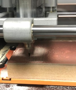
I initiated the process by milling the traces, and at the very first trial something was not quite right.
The pads representing the ground were not engraved. After discussing this with Hashim, it turns out that I forgot to change the settings for the thermal Isolation in DRC which basically substracts the pads from the signal polygon, in my case, the common ground.
Now processing the files again for the milling would have been a long process again, but I am using FlatCam, So I only needed to regenerate the Gerber files again! Ha!
Trying the milling again, and the GND pads were engraved this time. I also drilled the holes for the connectors.

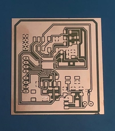
And finally the outlines, hence the final board:
Then came the soldering stage, which admittedly, wasn’t quite easy either. But hey! its finishing the hard tasks that brings the most satisfaction!
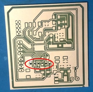
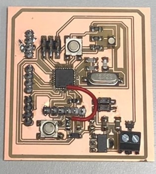
One of the reasons why soldering took a good chunk of time this week, is the placement of some components, for example, my FTDI traces were right in the middle! which is a big mistake. Thus, I turned it into a through hole connection and drilled the holes myself using the manual drill.
Another difficulty I faced in soldering this board, was the Atmega 328 chip itself, the pins were very small and hard to solder one at a time. Thus I used a technique where I spread solder on the pins and removed the excess with the de-soldering pump.
And finally, this is how my board looked like.
(The red wire connected my reset resistor to the reset pin of the atmega, the trace was cut when I tried drilling the holes of the FTDI).
My trials to test the operation of the board can be found on the Embedded programming week.
For the group assignment, we are using different equipment to measure voltages and signals of our boards. We are documenting out work individually since everyone worked on their own boards. Here is the group page with all our work combined.
Here I am using the Attiny 44 board I designed this week, and I am measuring the input voltage, and the voltage change of the LED blinking with a 1 second delay rate.
I connected the alligator section of the probe to ground, and the “signal” part to the pin I am taking my reading from.
It can be observed with each blink of the LED, the voltage goes up to 5 V and back to Zero.
My files:
