
The Fab Academy is responsible for
I am a Fab Academy instructor, responsible for
Signed by committing this file in my repository, (Abdullatif Albaroudi)
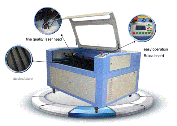
Kerf is defined as the width of material that is removed by a cutting process. It was originally used to describe how much wood was removed by a saw, because the teeth on a saw are bent to the side, so that they remove more material than the width of the saw blade itself, preventing the blade from getting stuck in the wood.

When cutting parts on a CNC plasma or laser machine, you want to produce accurate cut parts, with final dimensions as close as possible to the programmed shape. So if you program a 6” by 6” square, and the plasma arc removes 0.200” of material, as it cuts, then the resulting part is going to be 5.8” by 5.8”. So the actual tool path has to be compensated by 0.100” to the side of the programmed path, all the way around the part.
Rather than re-program the part at a different dimension, the CNC will take care of this automatically just by telling it which direction to offset, and by how much. Most modern CNCs take the actual kerf amount and automatically offset the tool path by 1/2 of that amount, so that the finished part comes out very close to the programmed dimensions. That is why the kerf value is often referred to as “kerf offset”.
source:
https://www.esabna.com/us/en/education/blog/what-is-cutting-kerf.cfm
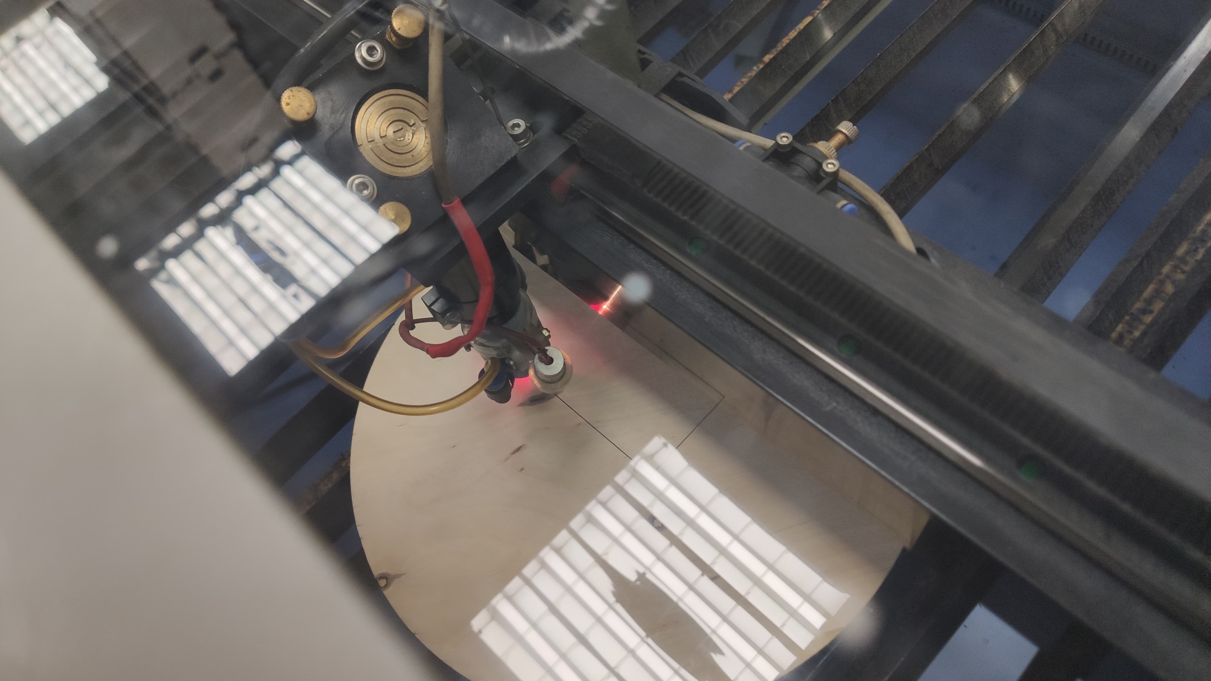
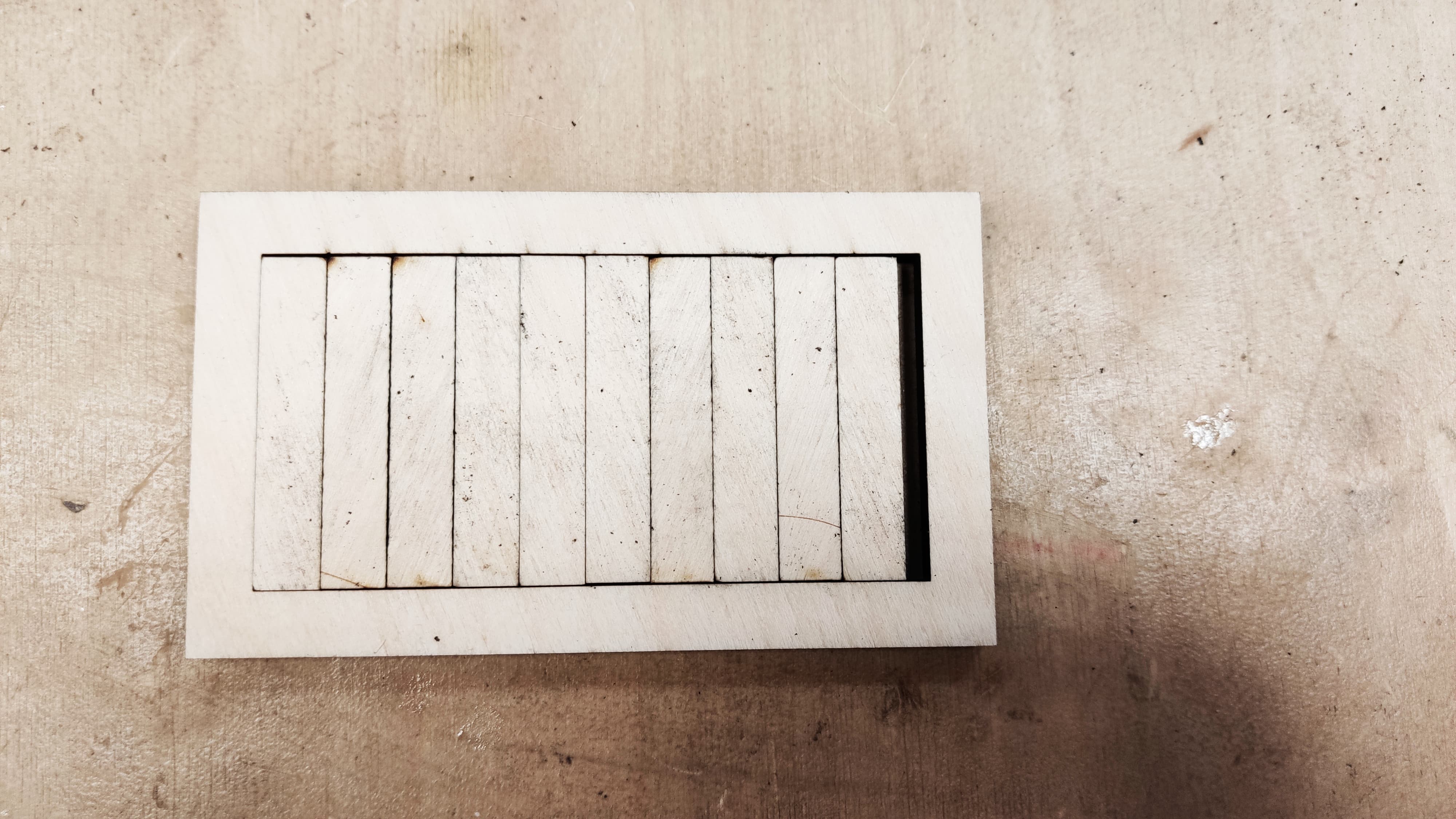
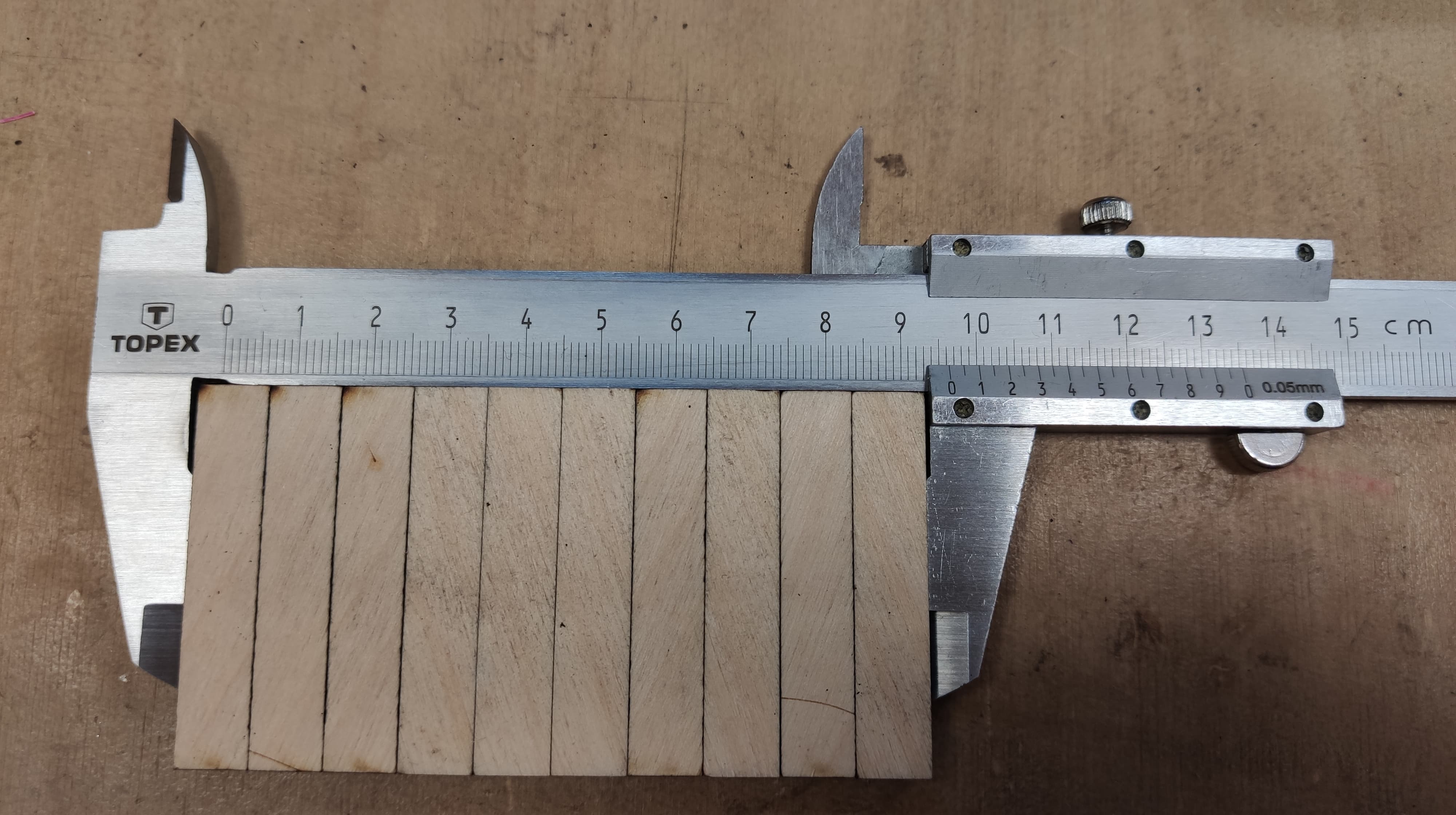
During the tests with kerf we used plywood with a thickness of 3 and 6 mm, which is the material most often used in our Fablab. The test was carried out by cutting out 10 equal-sized rectangles placed next to each other and calculating the difference between the design and the cut out elements on the laser plotter. For the test we used the best possible settings.
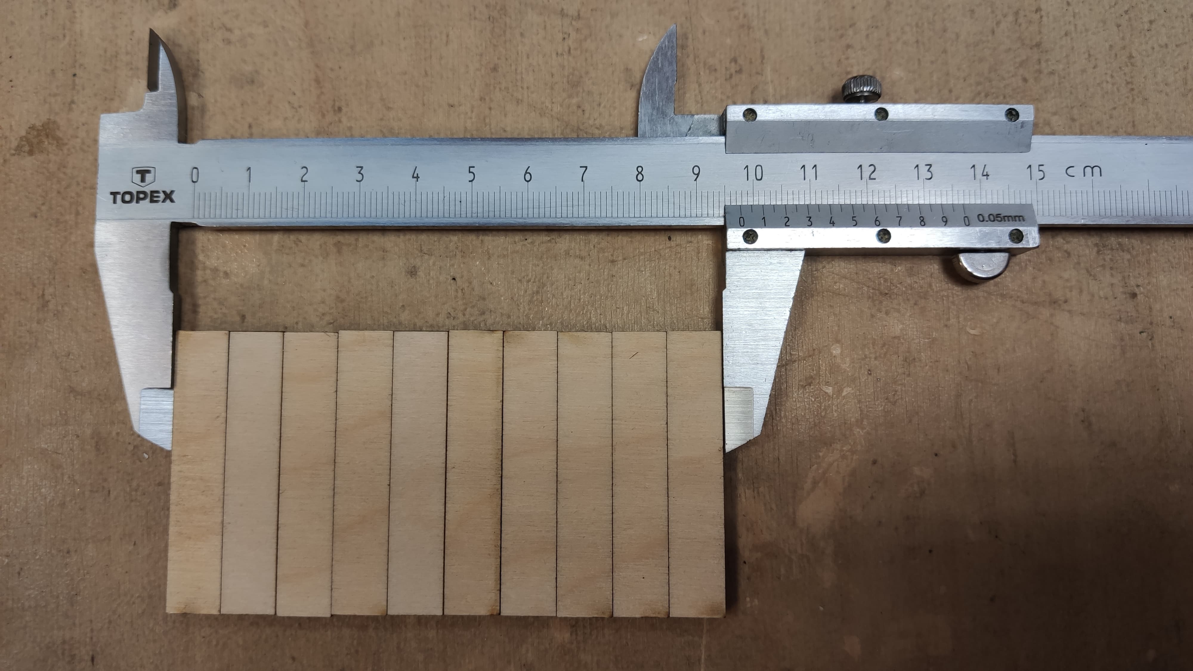
The results on 3mm thick plywood did not surprise us. The value that came out is more or less in line with what we assumed. After cutting ten 10 mm rectangles we came out with 97.7 mm of material, i.e. the value of burnt material came out with 2.3 mm divided by the number of cuts (11) gave us kerf value 0.2 mm.
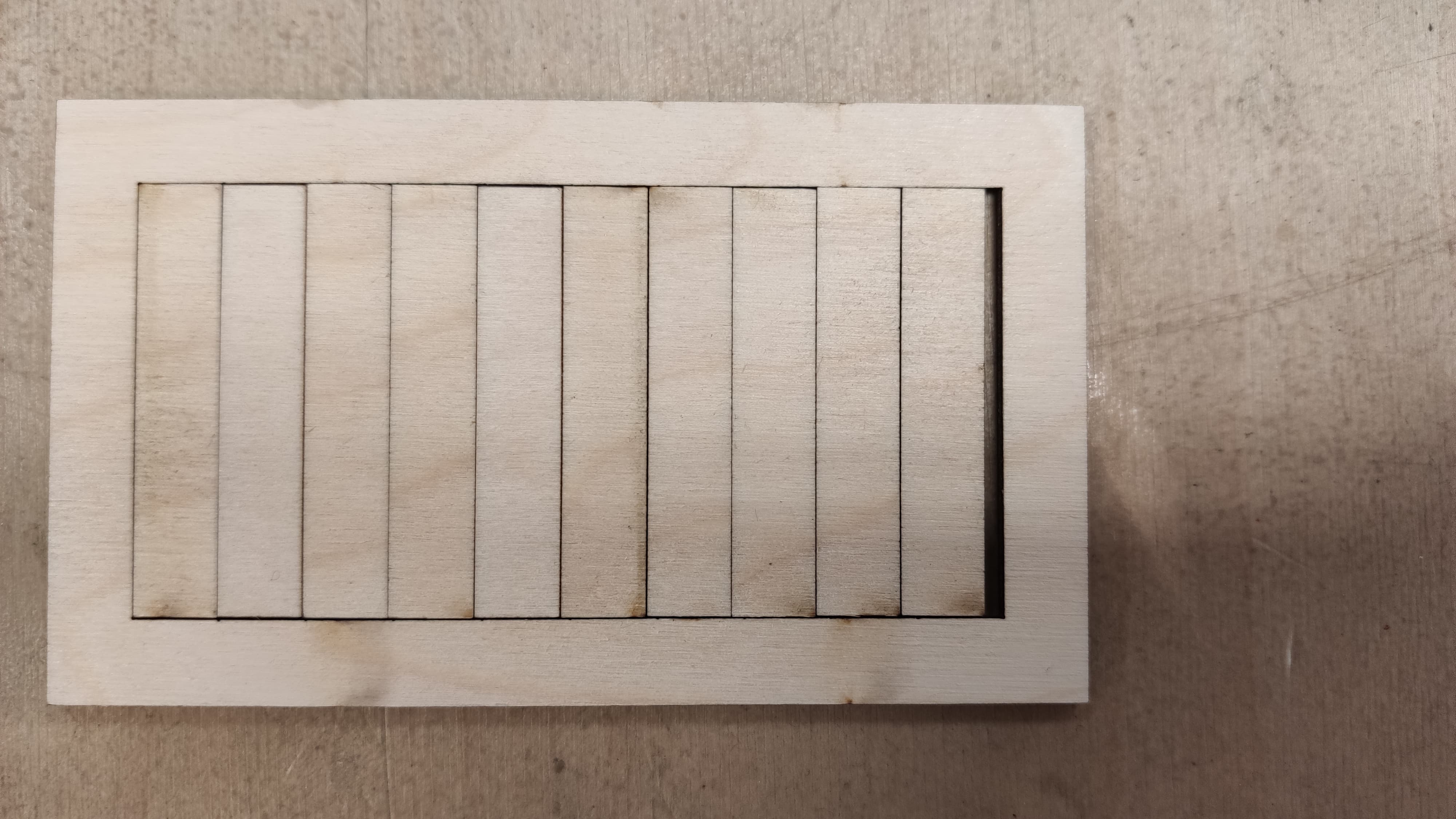
When it comes to 6 mm thick plywood we set Speed 8 mm/sec Power 60%.
Below is a table with laser settings tested by our fablab community.
There is no standardized way of producing PCBs in our fablab.
Some users sub-contract more complex layouts and some of them
are pickled in a friendly hackerspace or have their own PCB
milling machine.
In order to produce the first PCBs we came up with machines
on which we could do it... and it turned out that we had quite a few:

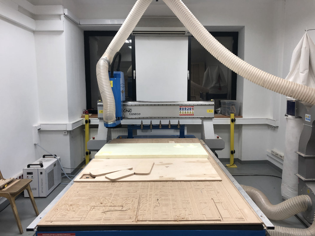
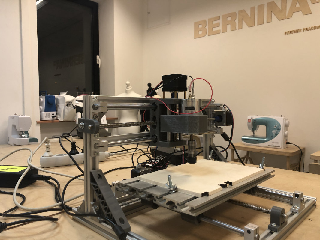
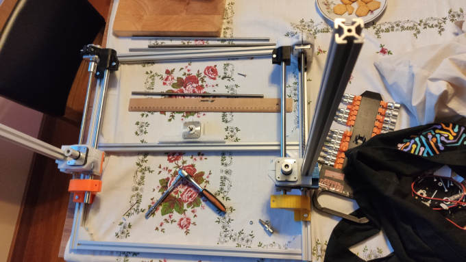
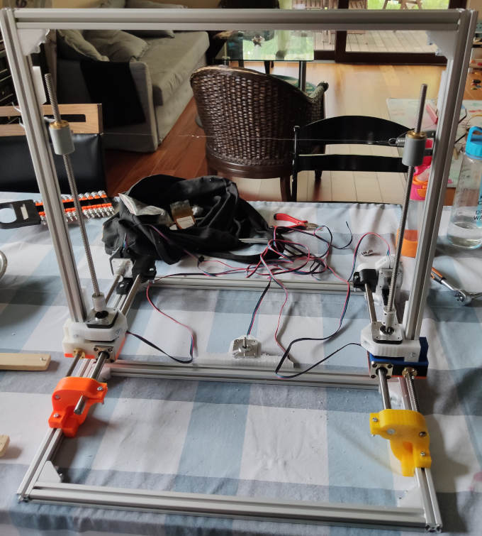
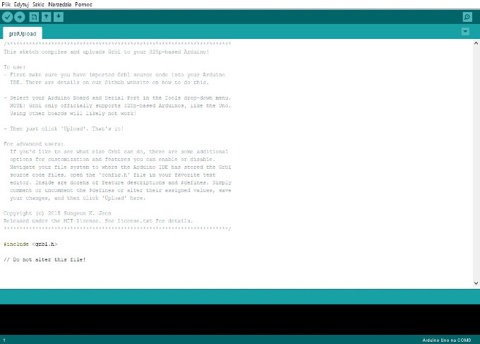
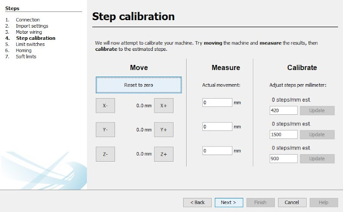
After selecting the milling machine, we needed grblControl software installed on a computer with windows system, a very simple software for basic operation of the machine. The first thing after installing the software and understanding the basics of operation was to level the surface which in our case was made of plywood with a 3.175 mm diamond cutter.

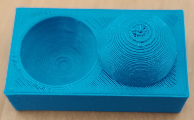
In fablab we have two types of printers: FDM and SLA. In the description below I will describe the operation and design principles under Zortrax M200, Formlabs 1+ and MAKERBOT. For testing I used a file made available to ctrV on thingivers.
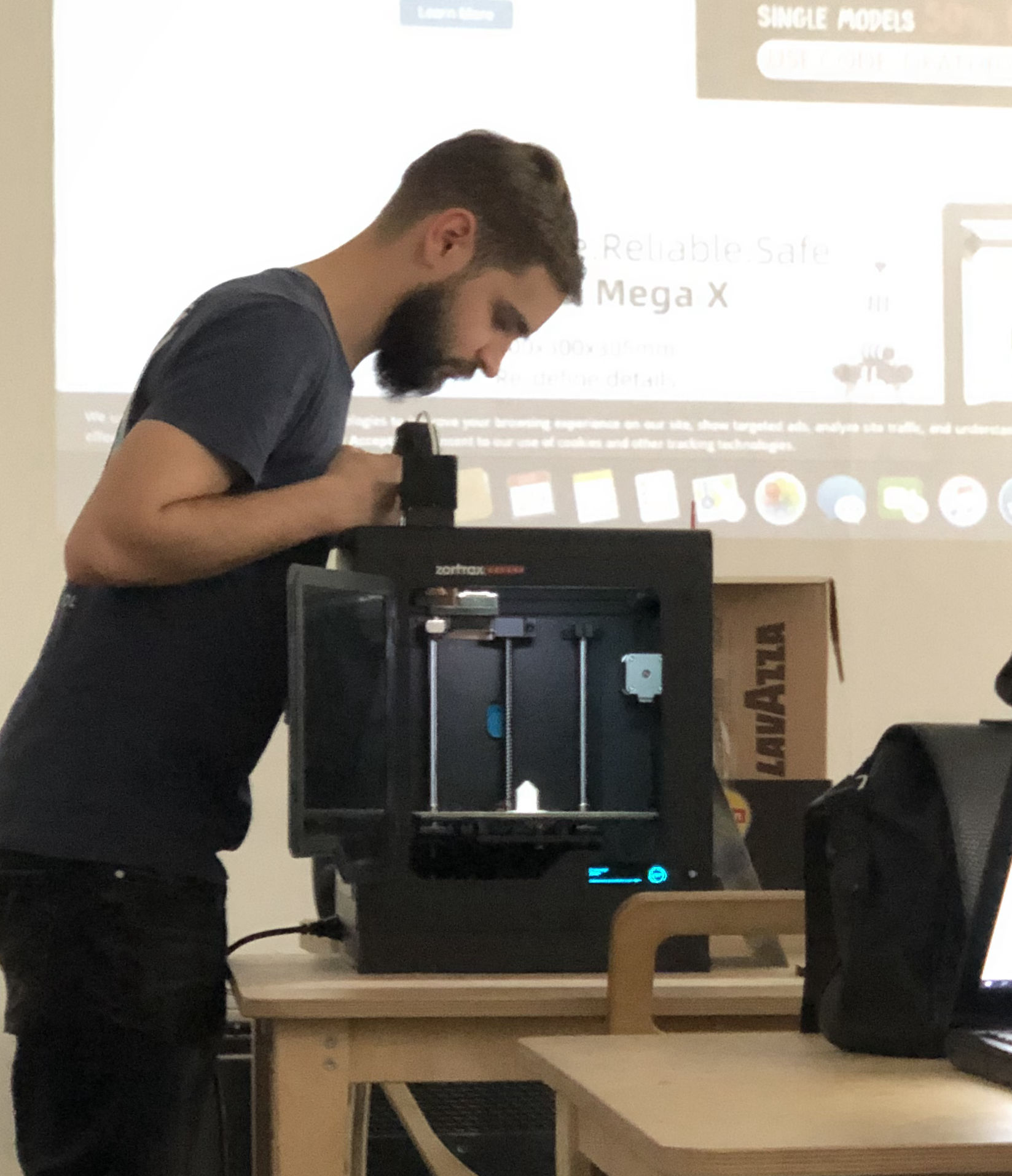
Zortrax is a Polish company that is very well known in the market
for creating armoured printers that may not print the most
beautifully but print almost always, and if they do not print
it is your fault. Over the years these printers have had a very
closed infrastructure, so only the manufacturer's materials could
be used and the software was very limited. At the moment, after
many consultations with users, it is possible to print from any
material to save presets and turn off the raft (which can only be
useful for quick test prints at a perforated table).
On the manufacturer's website there is a program for Zortrax,
called Z-Suit ,
which is on Win and Mac. For installation we will
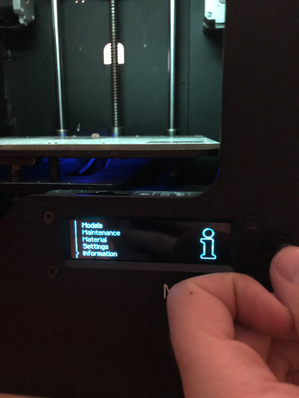
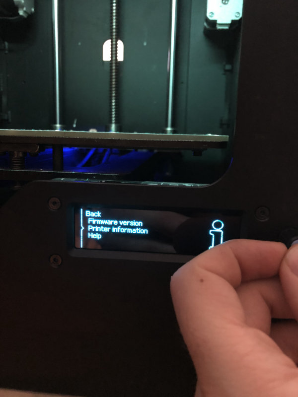
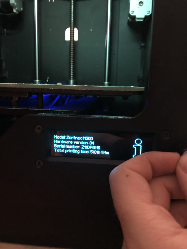
need a serial number, which is on each printer in
Information=>Printer Information (uff this printer has
been running for over 5k hours and still works great).
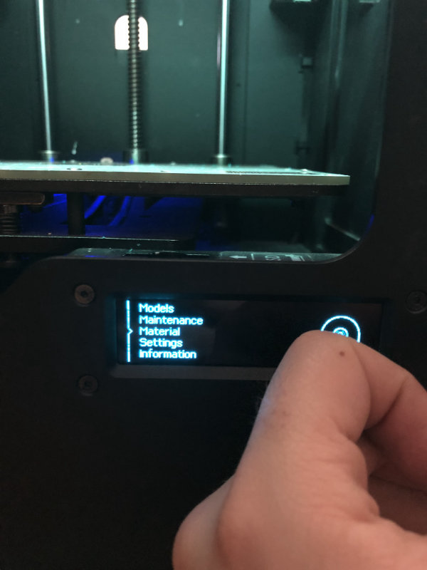
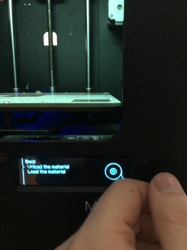
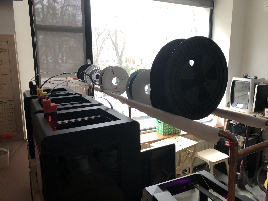
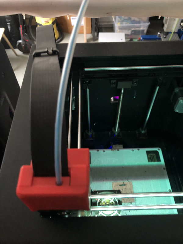
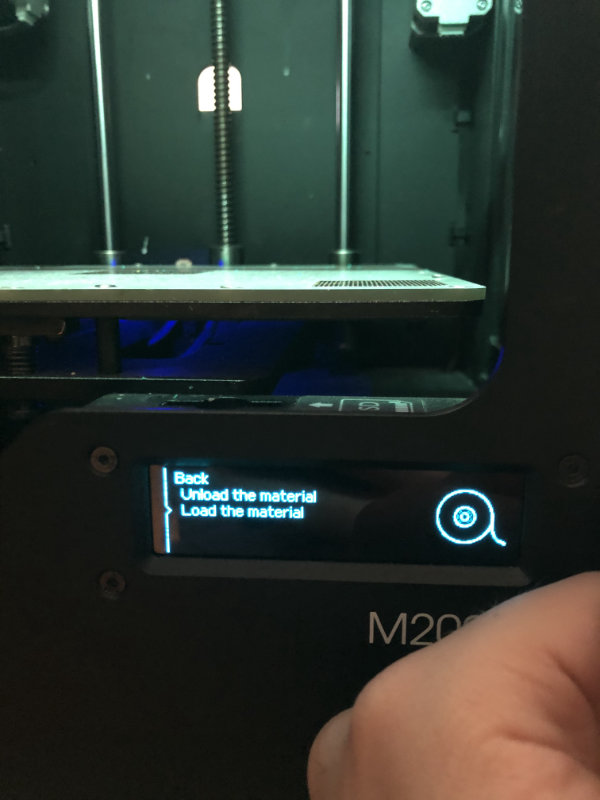
Work area: 295 x 195 x 165 mm
Materials: PLA, TOUGH PLA
Software: MakerBot Print,
Layer height: 100-200-300 microns
Dimensions: 528 x 441 x 410 mm
Weight: 18.3 kg
Operating the slicer for this printer is trivially simple,
but unfortunately it also has its limitations due to the
few options available to users and the simplest options
such as print settings are hidden.
Select a file and upload it by drag and drop or choose from import.
Choose a printer from the network (after the ip address)
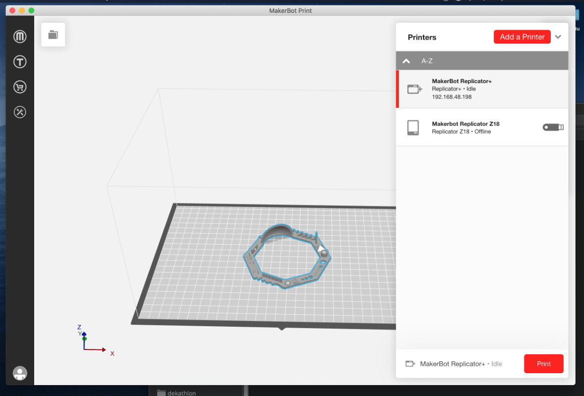
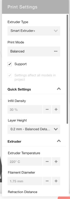
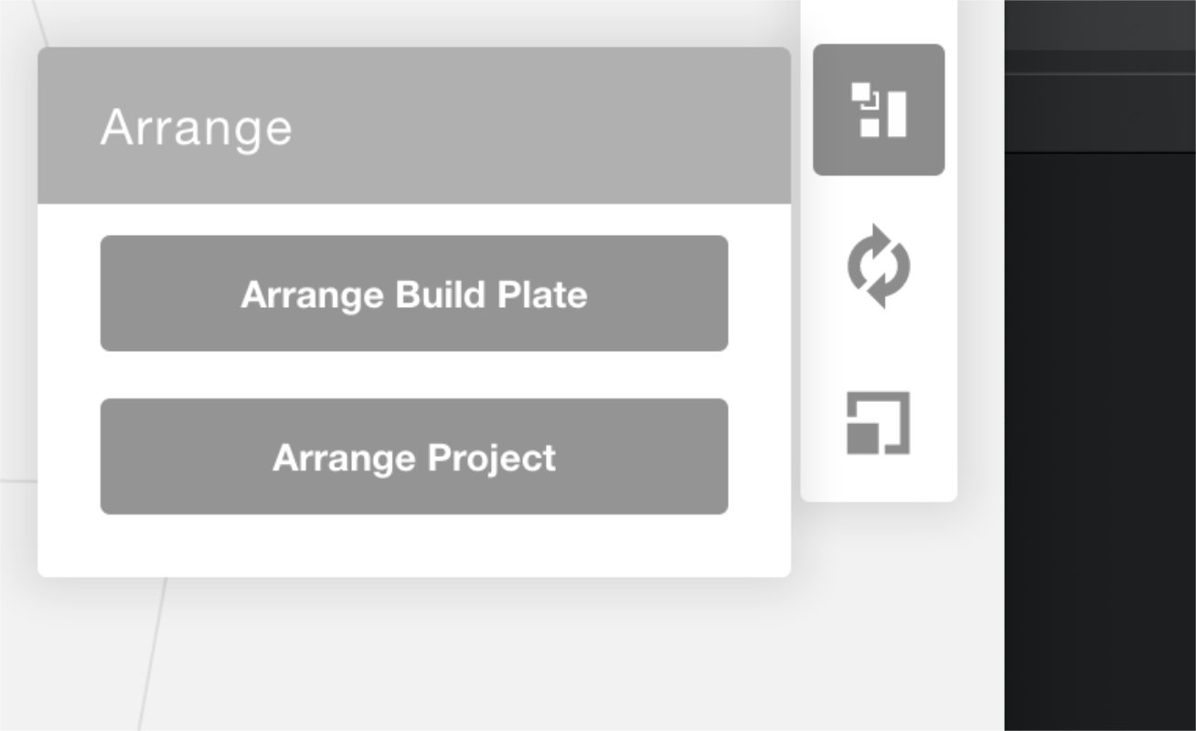
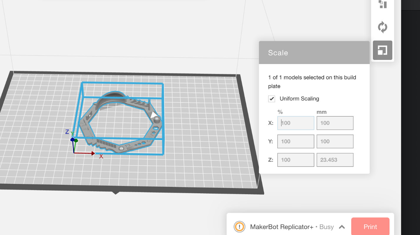
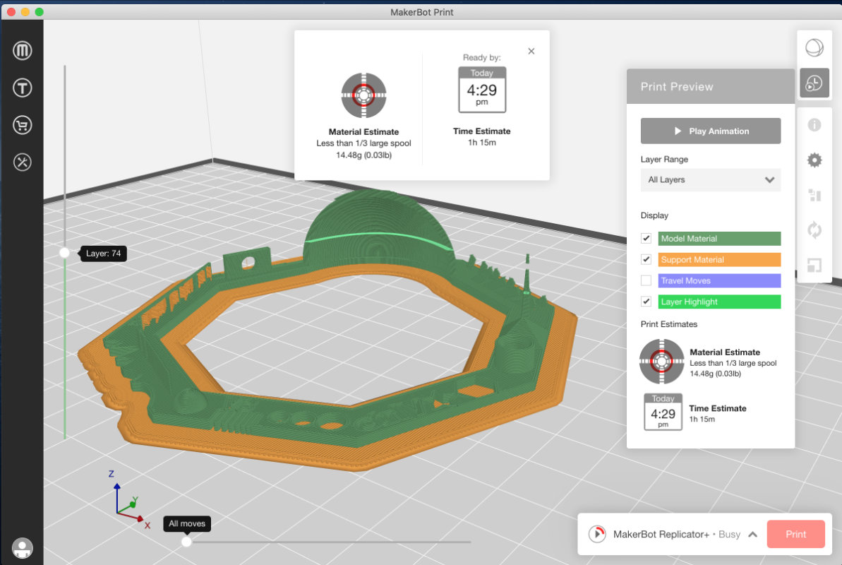
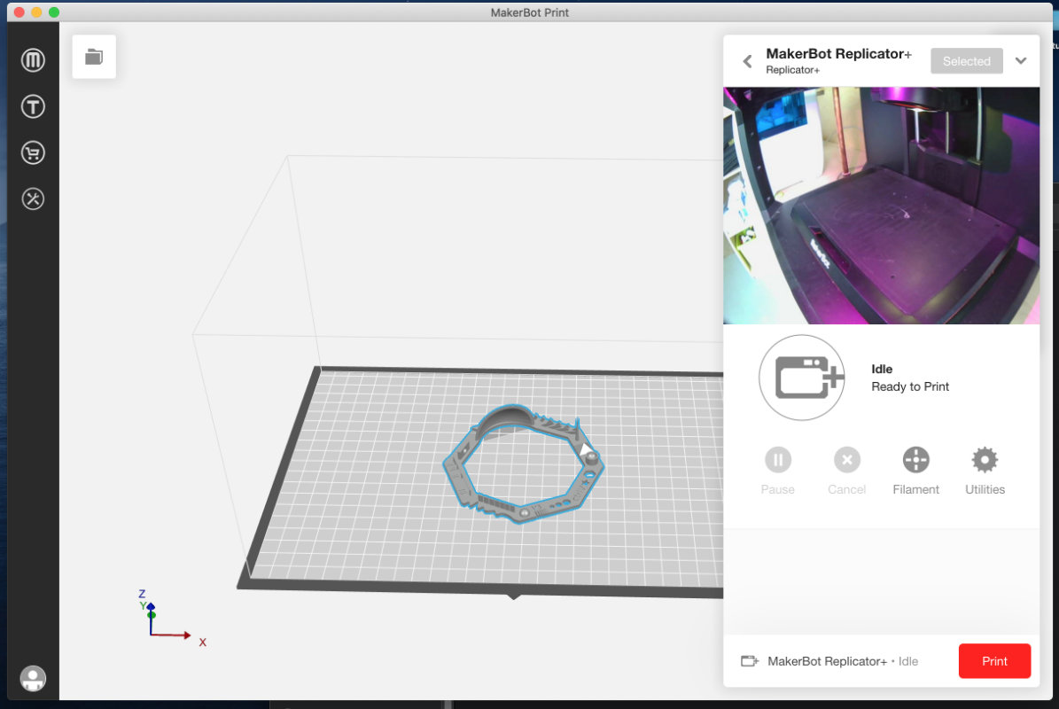
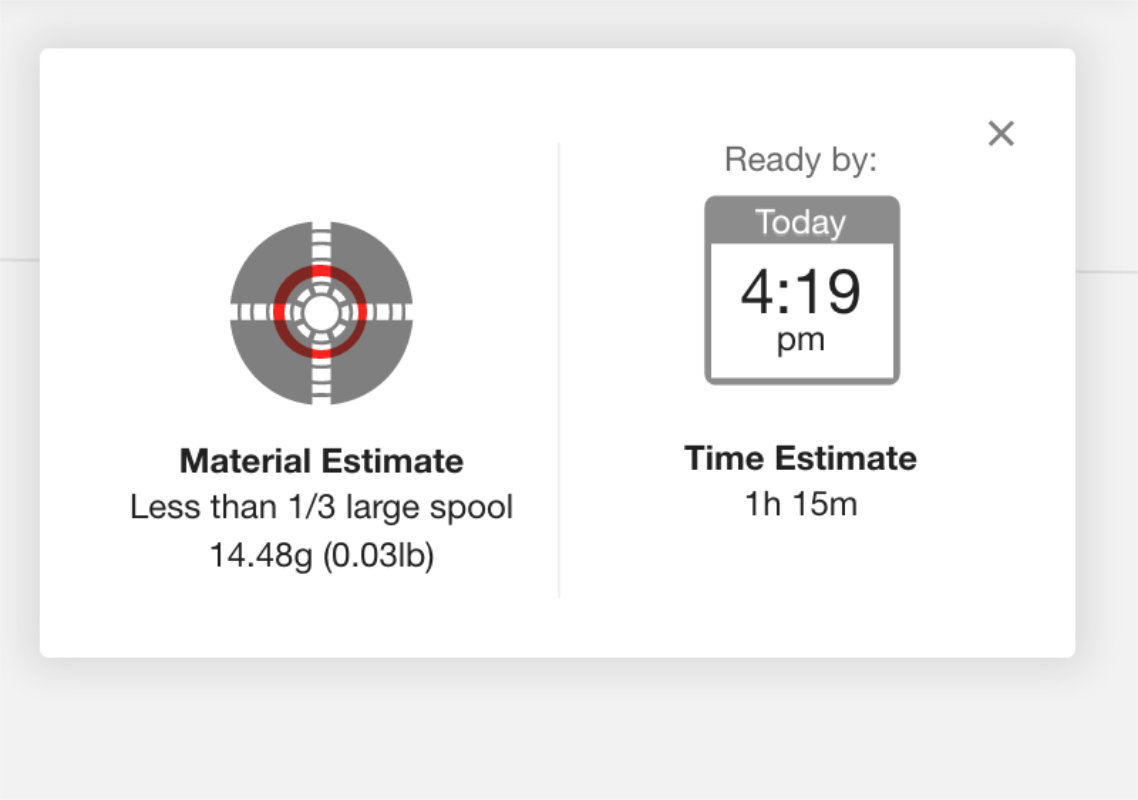
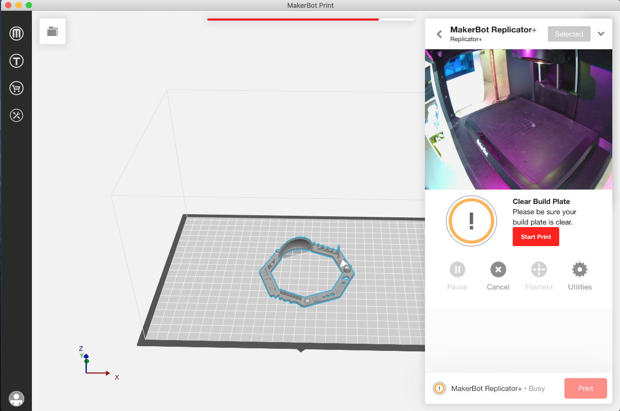
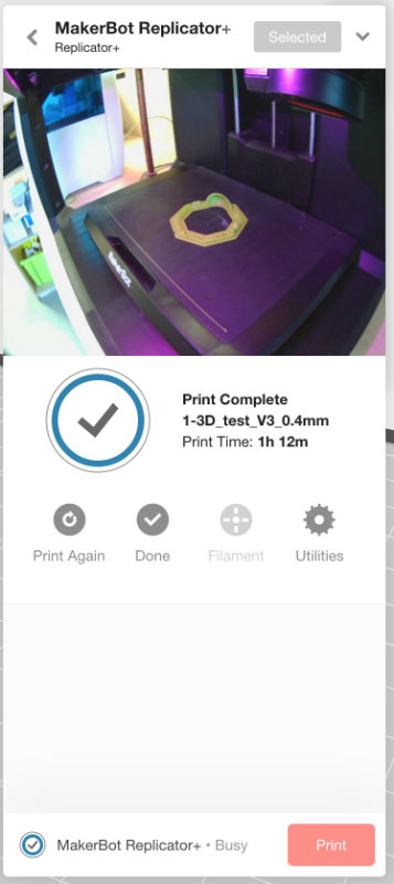
Most of the Slicer works very similarly, it is enough that we know the basic
functions and naming and we can print on practically any printer, so before
I take a look at the detailed operation z-suit will describe some important settings.
Model positioning
A very important option depends on how long the object will
print and in which plane it will be stronger and more resistant to
particular stresses. More info here
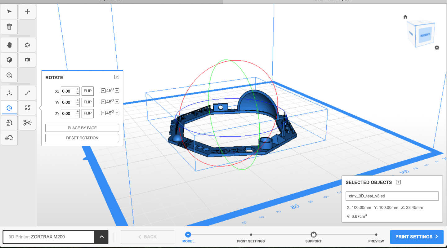
For FDM, the top surface is smoothed by the extrusion
tip, the surface in contact with the print bed will
usually be glossy and the surfaces above support structures will have support marks.
Material types:
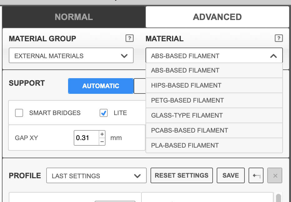
Basic materials used in our Fablab
PLA
ABS
HIPS
PETG
Layer height:
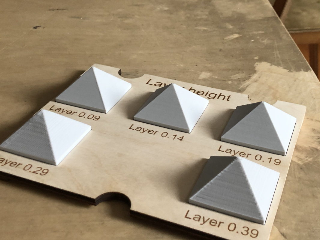
The quality in the Z-axis depends on the height of the layer.
It has been assumed that layers from 0.29 mm upwards can be easily
set for prototypes and models without much detail. Thanks to the high
layer height we can quickly have the object for testing and further
modifications. In addition, the printout can always be post-processed
and the ideal surface can be obtained. For more detailed prints we use
smaller values up to 0.6mm on FDM printers.
Unfortunately, a low layer extends our waiting time for the final product,
so it is always worth considering why we will need a printout. Below is a
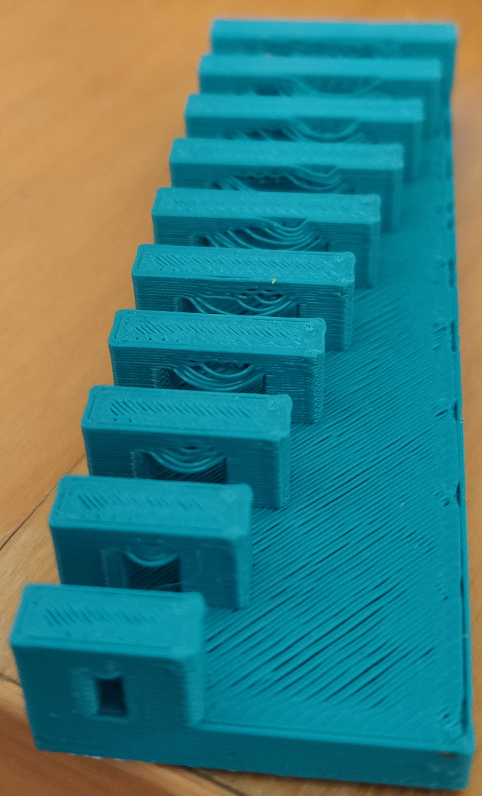
picture of a board with sample layers and printing times on zortrax m200.
Infill:
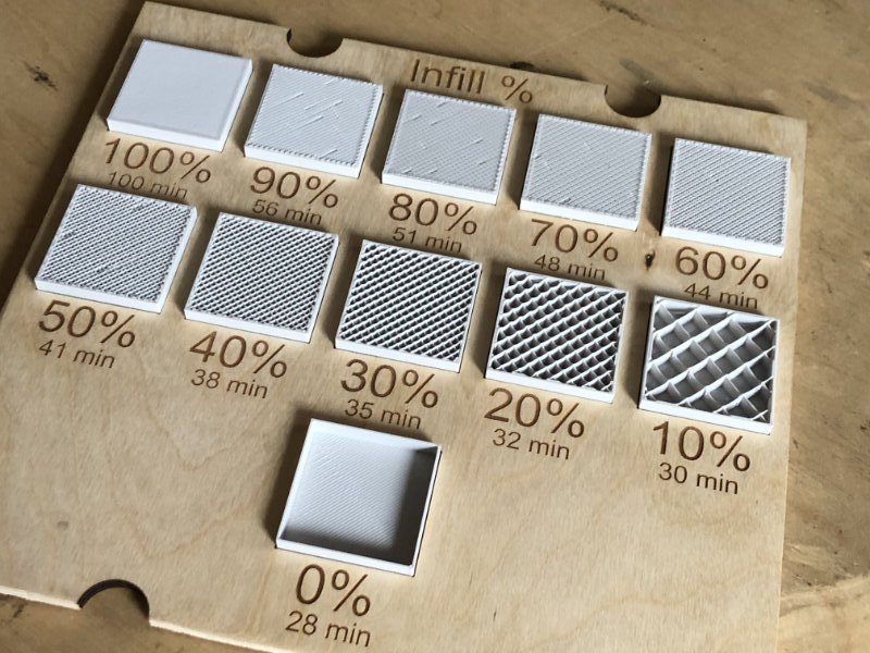
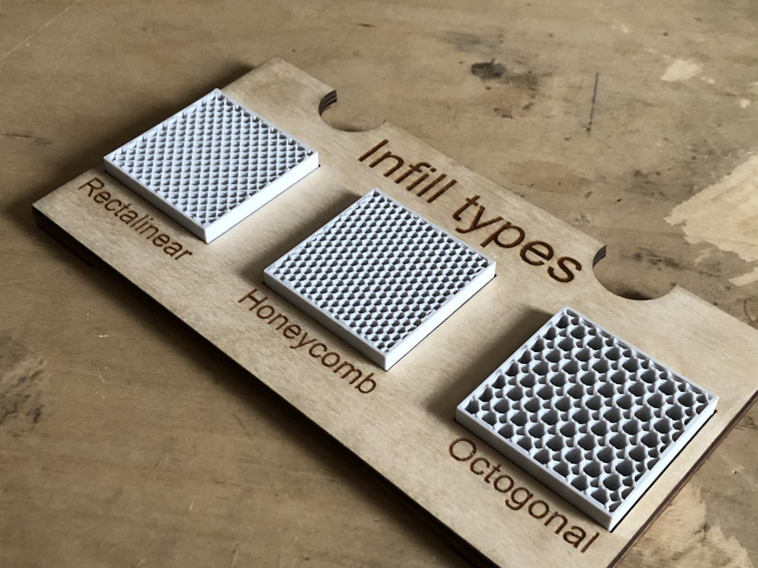
Infill, i.e. percentage filling of the object. You might think that the
bigger the filling the stronger and stronger the print. Fortunately,
this is not the most optimal infill for commercial objects ranging
from 15-25%, and the stronger the printout is 40%.
But why not 100%?
Large fully filled objects are more fragile
fully filled objects are susceptible to cracking and shrinkage of the material
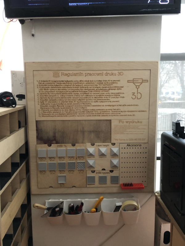
3D printing rules in our fablab
Before printing
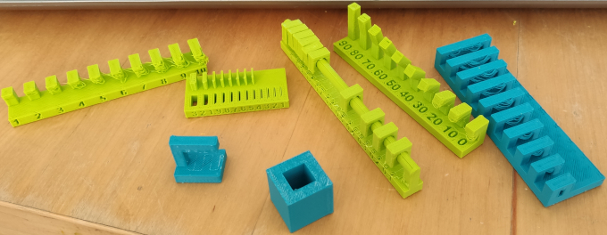

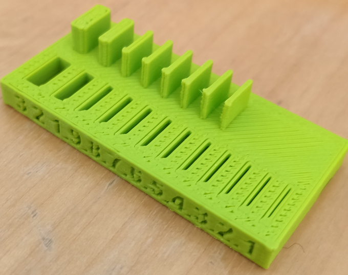
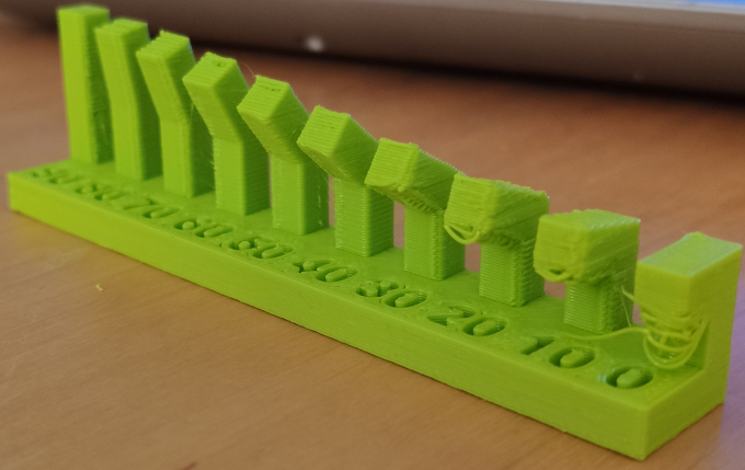
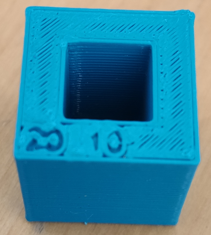




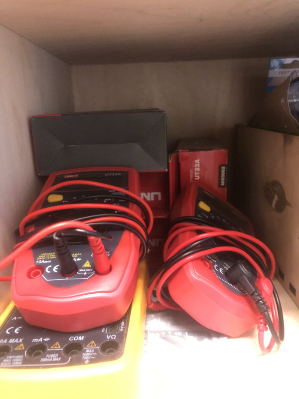
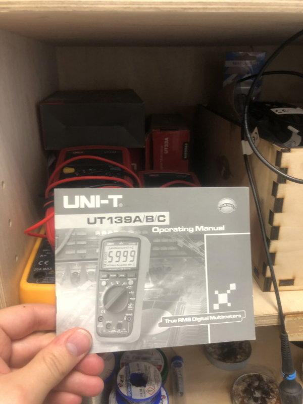
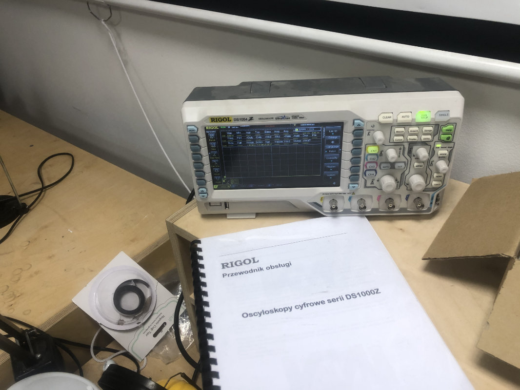
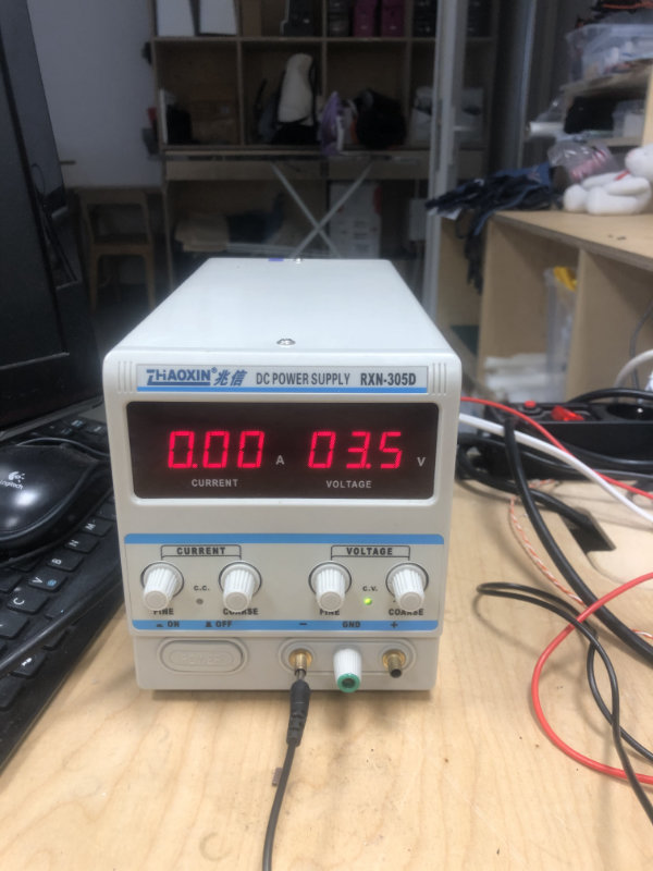
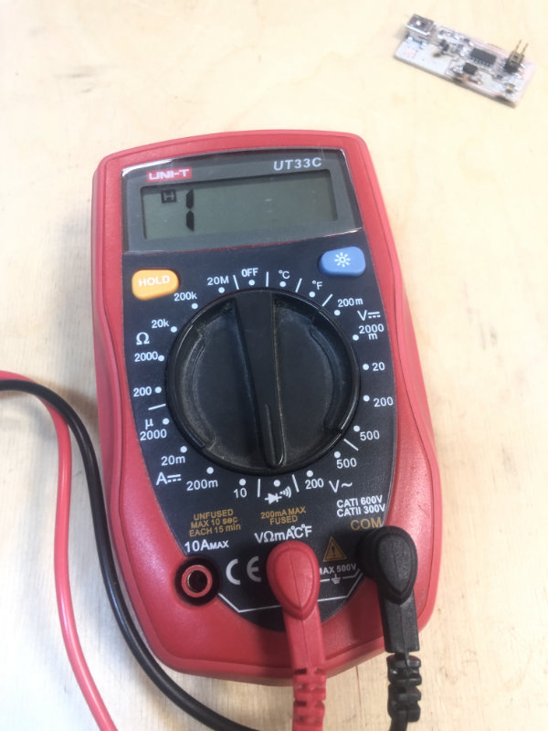
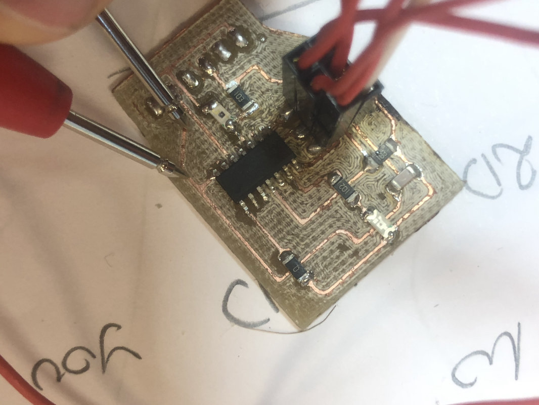
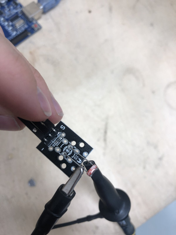
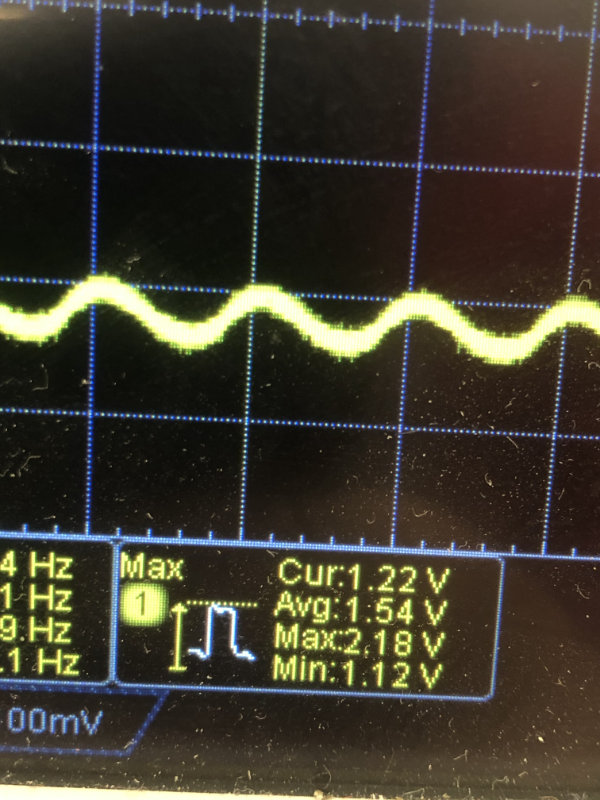
Use the test equipment in your lab to observe the operation of a microcontroller circuit board (in minimum, check operating voltage on the board with multimeter or voltmeter and use oscilloscope to check noise of operating voltage and interpret a data signal) Equipment used in testings:
Wikipedia

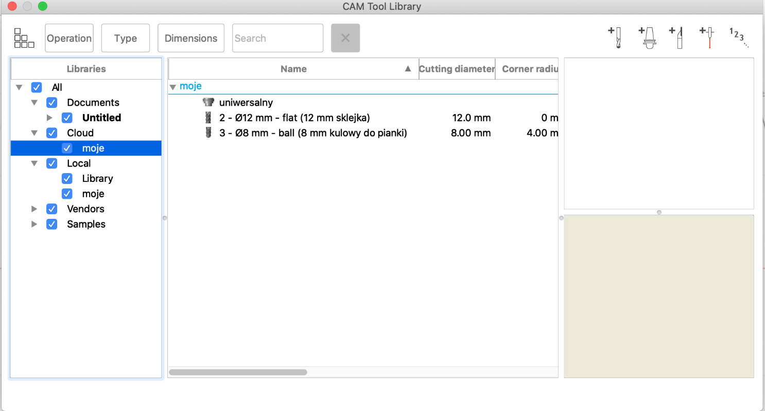
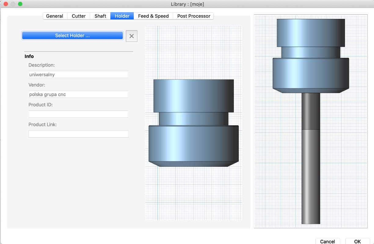
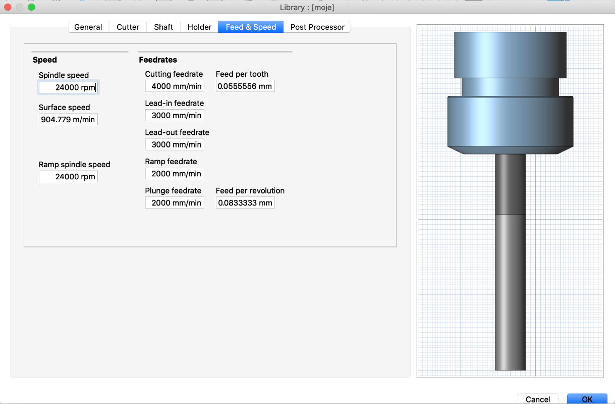
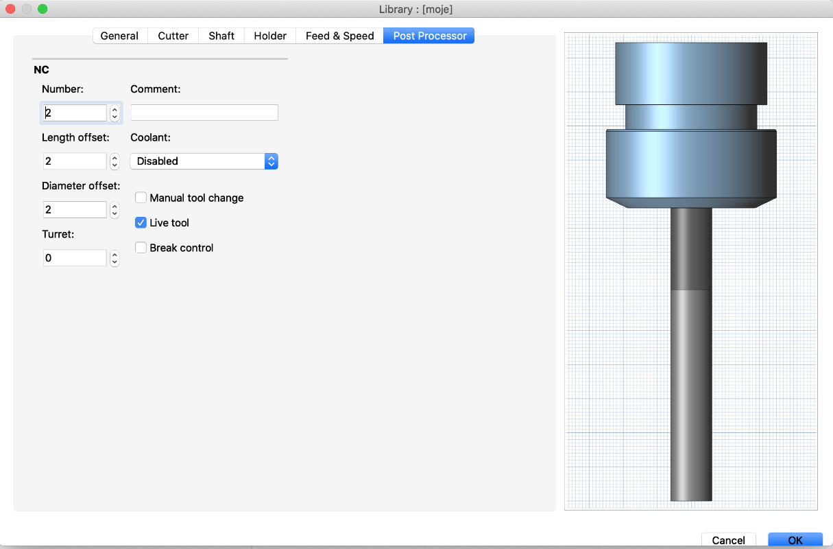
A few words about our milling machine:
the tool wall at our cnc workshop is very useful for organizing tools
Our task for group in this week was to test the performance and developement workflows for other architectures.
To make this assigment undestandable for all it is the best to 1st show what kind of different architectures we can use in this assigment and most importantly what is the architecture of microcontroller.
 The Von Neumann architecture consists of a single, shared memory for programs and data, a single bus for memory access, an arithmetic unit, and a program control unit. The Von Neumann processor operates fetching and execution cycles seriously.

AVR Microcontrollers on Arduino UNO
I programed my board and tested on an Arduino in virtual enviroment in Tinkercad Cirtucts on www.tinercad.com. Since I have already a board made there I decided to reuse it. I will make the old board use the LED supplied already plus additional one and say "HELLO WORLD" in Morse code after pushing the button. So one LED on will be a short signal and two LEDs on will be a long signal.

So 1st thing that I have to do is to add new LED to the current setup.
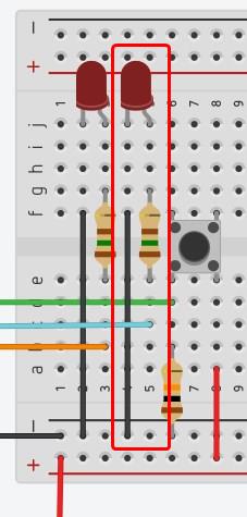
The new LED is connected with the board via turquoise wire and thats make the board complete and ready to get programed.
All is left is to write the code... and yeah, learn Morse Code!!!
So lets 1st look at the Morse Code Graph[1].
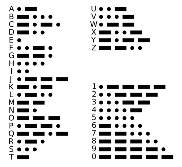
I will use this graph as a reference for making the code.
So lets dig into code! The code we will use C language.
I will start from reusing the previous code so I will simply add the new LED as an output on PIN number 4 (turquoise wire).
		const int buttonPin = 3; //Pin for the button
	const int LEDPin = 2; //Pin for the LED
	const int LEDPin2 = 4; //Pin for the LED2 (added line)

	void setup()
	{
		pinMode(buttonPin, INPUT); //setting the input PIN
		pinMode(LEDPin, OUTPUT); //setting the output PIN
		pinMode(LEDPin2, OUTPUT); //(added line)
		Serial.begin(9600); // Serial console setup
	}
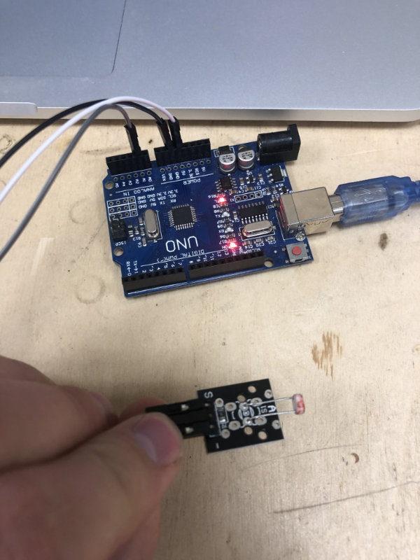
							int photo = A1;

							void setup() {
							  Serial.begin(9600);
							}

							void loop() {
							  photo = analogRead(A1);
							  Serial.println(photo);

							  delay(200);
							}


Output devices

(We changed mA to A)
Pmin = 4.8 * 0.0188 = 0.09024W
Pmax = 4.8 * 0.023 = 0.1104W(We changed mA to A)
Pmin = 4.7 * 0.0211 = 0.09917W
Pmax = 4.7 * 0.075 = 0.3725WInterface and application programming


Networking and communications

Molding and casting

Wildcard week


