Using Eagle
Here is our group works : week6
It was time to install and use the Eagle from Autodesk for the first time. It looked good because it seemed to be connected with Fusion 360 at a distance. The Eagle could be divided into a control panel, a Schematic window, and a Board window. I designed Hello.fdti.44 along Eagle Tutorial.
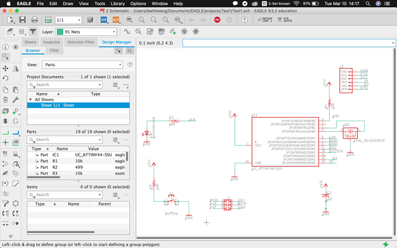
This is where components are added and each component is designed to be connected. Here I was forced to receive large quantities of components from Sparkfun because my MAC did not recognize the Fab Library. And I found the same components one by one... LOL
This is the first time a component was inserted and connected. There is a problem here. It is that the line is so thin that it may or may not come out properly.
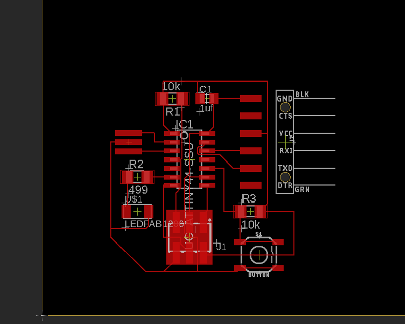
The lines are thin and the spacing is so narrow that it is almost impossible. The reason why I know that is because I checked the possible line with group work during Week 4! I overlooked it.
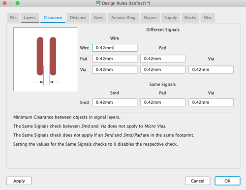
Realizing that, the design rules gave a gap of 0.42mm between Wire, Pad and Via.
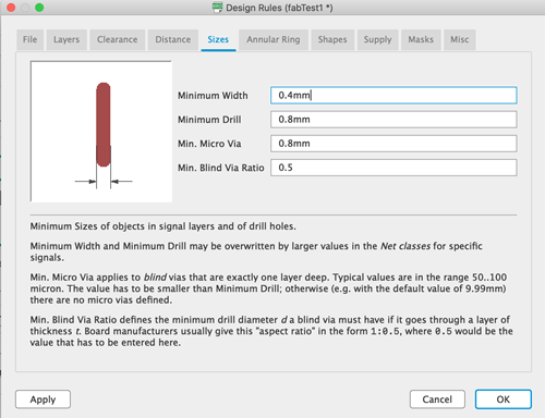
And the minimum width was set to 0.4 mm drill to 0.8 mm.

Before milling, you can check EagleCard to see if there are any real electronic circuit problems. Press ERC check to check for electronic circuit problems. There are some error messages and warnings, so it is necessary to check before milling.

Net was re-created by setting the width to 0.4mm. However, I saw a problem that is not marked as mm. If you know how to change someone's interface, please let me know.
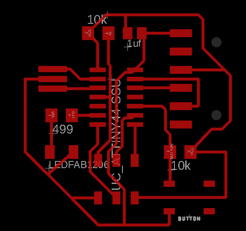
A new circuit diagram has been completed by 0.4mm and design rules.
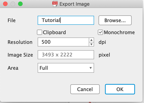
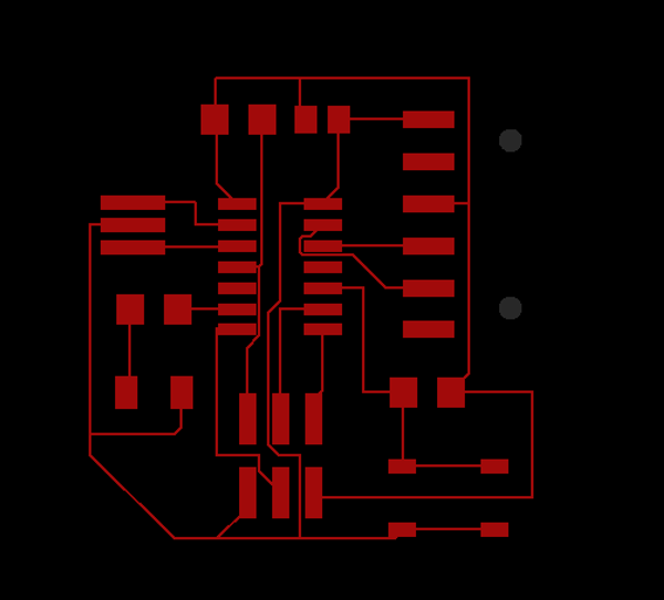
And made image PNG file pleasantly. I set up the dpi 500 from the tutorial and set Monochrome.
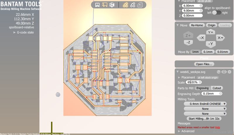
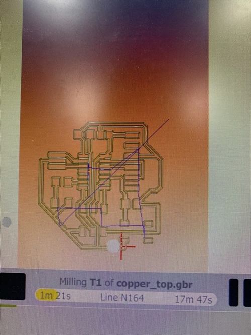
And this is the pre-milling look at Bantamtool.There are many problems here. Because the scale first came out different from what I did at Eagle.
The size of the end mill should be corrected if the preview shows the part that is not being milling with the red part. And if the gap in board design is too narrow, you can increase it by increasing the trace clearance..
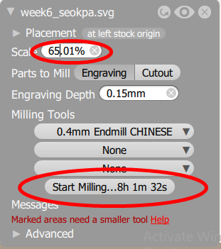
And if you look here, there's a change in scale (automatically changing) and the milling time... ...that's just what you do? It was similar to the meaning of.

So I gave up this image file and found another way.
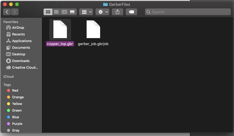
So I tried again by exporting to gbr file.
And I printed the circuit diagram in advance to see if the component size is correct.
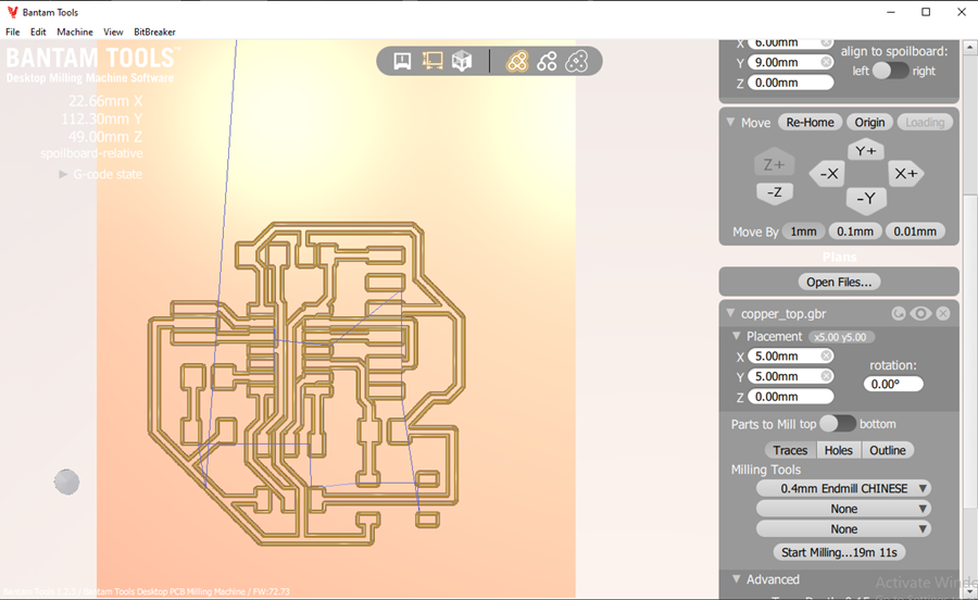
When I came back to Bantam tools, it was correct! The time was also satisfactory with 19 minutes and 11 seconds.
It's the process of milling.
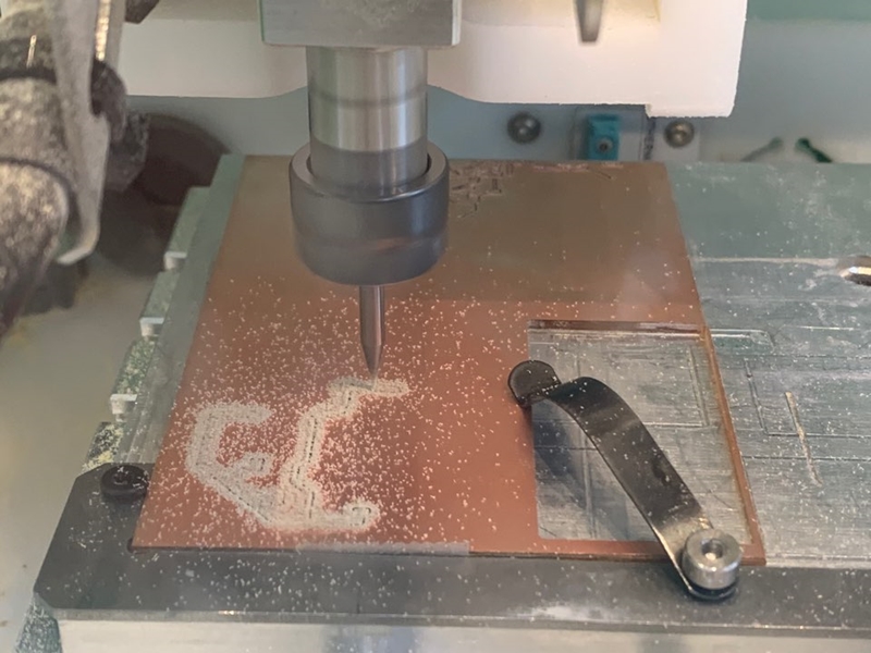
Milling~
Soldering and Programming
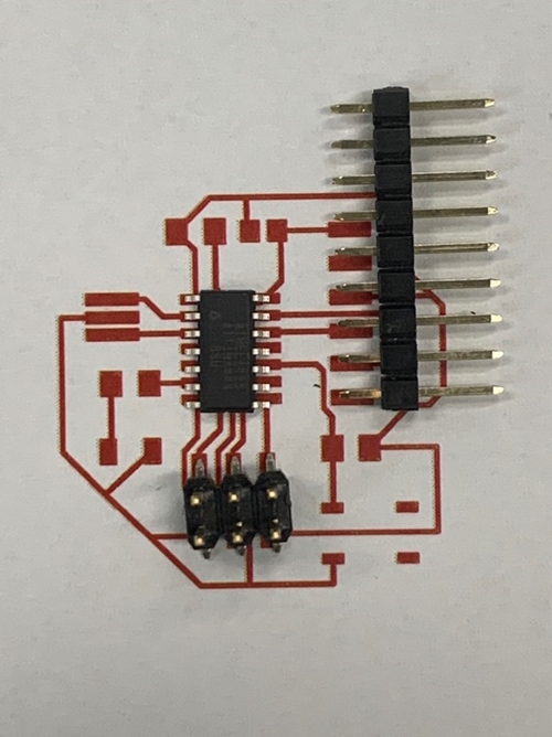
Find each component and prepare for soldering just like week4. Care points should be taken to ensure that components are correctly oriented and soldering. It then begins by reminiscing the conditions of soldering (injecting lead when the appropriate temperature rises) that made a mistake in the fourth week.
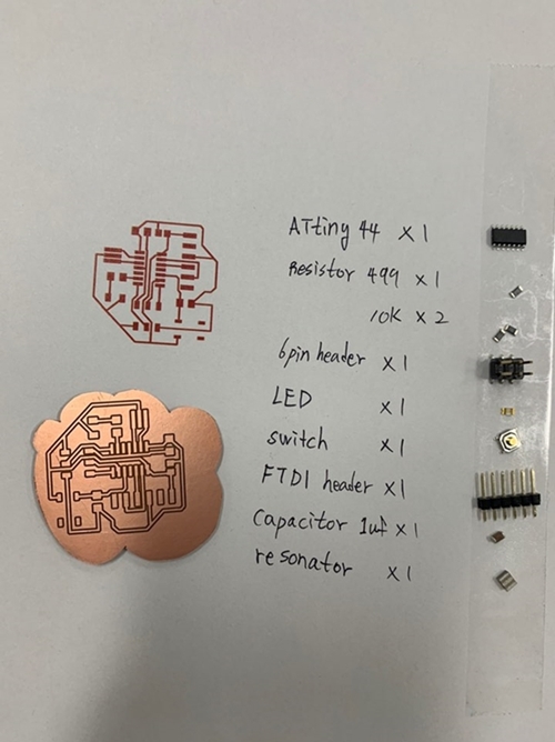
Check the number, location and direction of each component before starting soldering!
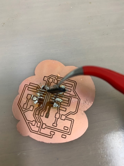
However, the 44 units were sold out and removed to the surface of the copper......
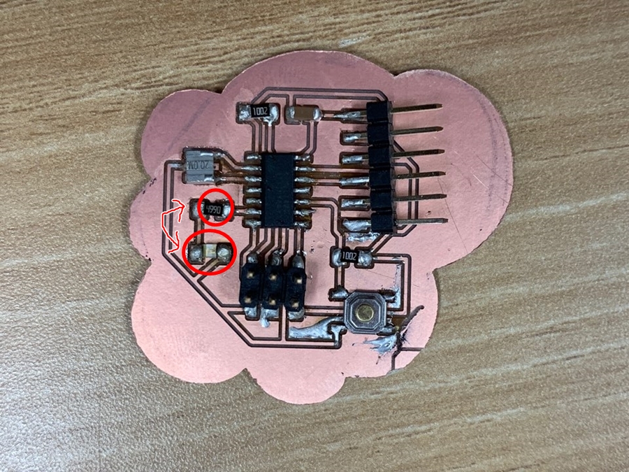
Well, but I figured out another problem after soldering. It was a misconnection of resistance and LEDs...
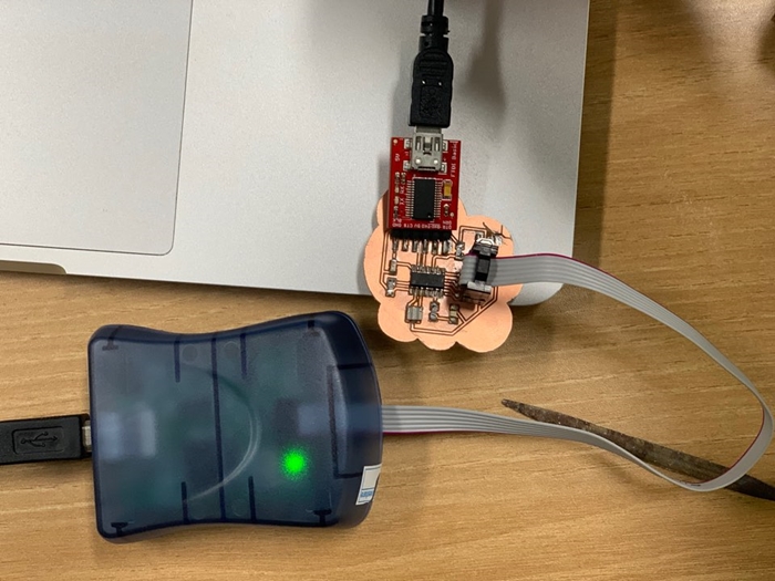
Anyway, I checked with ASP to see if there was any problem, but Greenlight came out.
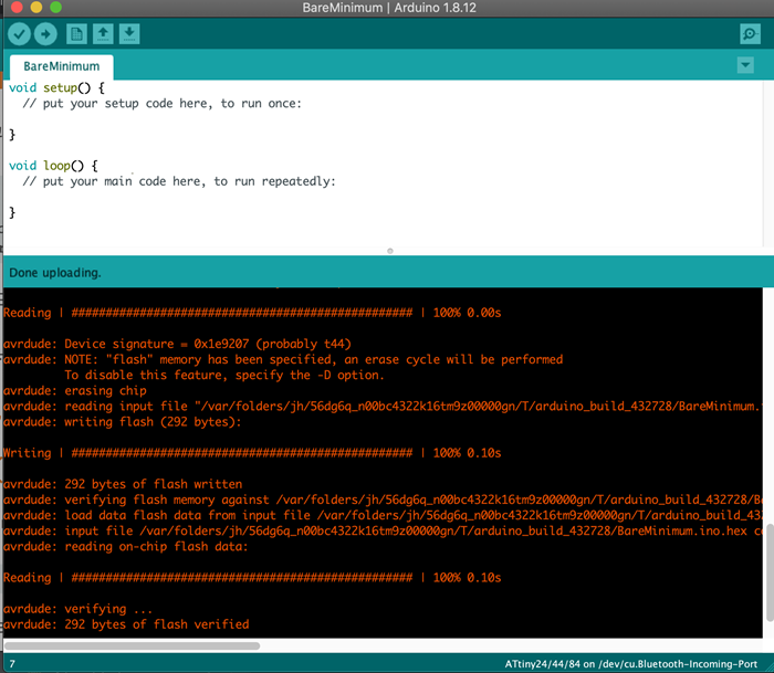
And we used BareMinimum among the examples in Aduino to see if there were any problems with coding. Clear!
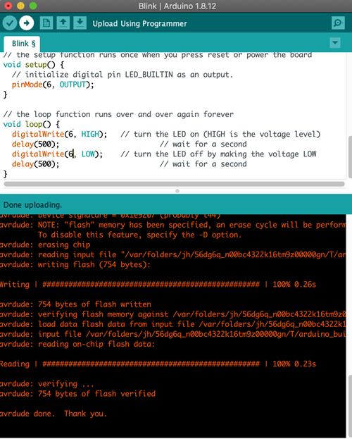
So, I wanted to turn on the LED, so I searched on Google, found the LED connected part of ATtiny, set the number accordingly, and programmed it.
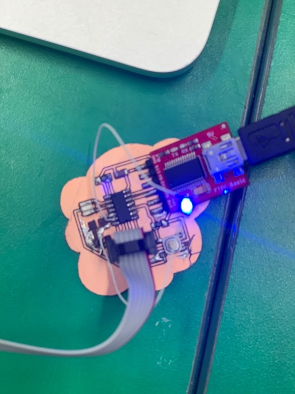
As a result, the fire came in. Why is there suddenly a white wire here? Because by taking it off... Milled lines fly and reconnect... LOL
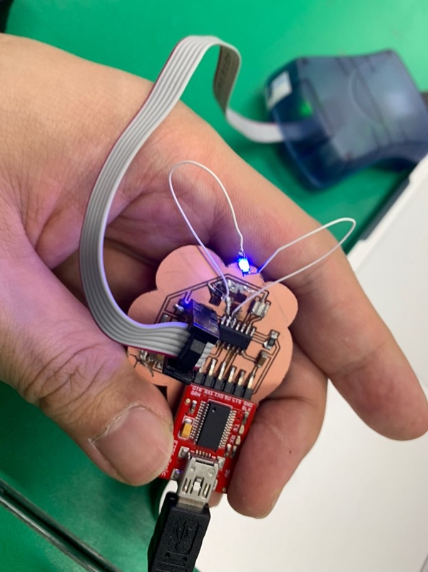
Anyway, I feel good that I did it in the process of solving the problem! I put the drawing file below.
: Download
Sch : Download
Brd : Download