Electronics Production
Federico, 20 February 2020
The assignments of this week were:
- group assignment: characterize the design rules for your PCB production process
- individual assignment: make an in-circuit programmer by milling and stuffing the PCB, test it, then optionally try other PCB processes
Link to the lesson. Link to the videolesson.
Working with fabmodules
This week I learned the way to mill pcb starting from png images. Someone could find it funny, but this method find his advantages for quickly prototyping. The first thing I noticed is that the method is very easy and effortless but we always have to take care of small bugs/configuration seetting that, if neglected, can make this experience a nightmare. We have to remember that even if working with fabmodules is very quick and easy, this is not the most professional way.
If you need mass production pcb and you’re going to sent your pcb design files to a pcb manufacturer (like jlcpb, easyeda, etc..) you will need to export Gerber file from your PCB cad.
MAIN PROCEDURE FOR ROLAND-MDX40 MILLING MACHINE
-
Go on fabmodules, also remember that the main fabmodules page is here
-
Input format
Select the .png format and the INLINE/OUTLINE png file of your board (the png that contains the traces of your PCB)
-
Output format
Once the image is uploaded and you can see it, choose the output format. In case you’re using a Roland mill machine choose “.rml”.
-
Choose the Process
If you have to mill traces, choose “PCB traces 1/64”.
If you have to mill the outline, choose “PCB outline 1/32”
- Select the Machine (in the right output windows)
Select the milling machine you’re using. In my case I selected MDX-40.
- Configure the milling tool speed [mm/s]
If you don’t have to produce 1’000’000 PCB in a day, a speed of 4 mm/s is fine and the results are good. Remember the old saying “quick and good doesn’t stay well together”. So here
- Choose your Milling rotation direction.
First of all take a look at this quick guide. You have to choose according to your need. Briefly:
Conventional: The workpiece will dissipate more heat decreasing the tool life and the chip are carried upwar by the tooth of the tool and fall in front of cutter edge,creating a damaged cut and some chips will be re-cutted.
Climb: The heat is dissipated from the chip only, that’s because the chip width start form maximum dimension and decreased as the tool is cutting the piece. This make also a cleaner cut of the chip, causing an increasing of tool life.
If you don’t have particular needs I think Climb is the right way to start and have good result (also Niel suggested it).
- Configure the main process dimensions.
-Offset Origin [mm]:
x0,y0,z0 are the offset origin where the board will start to be milled. Remember the outline and the traces rml file has to be the same offset origin. This is very useful to be very precise, without consuming too many space on the new copperboard. For exampe you can set the origin of the machine to the corner of the board and then the mill will start at (Xcorner+Xoffset,Ycorner+Yoffset) without any risk of exiting the copperboard. Remind that working with fabmodules and MDX40 the origin point corresponds to the lower-left hand corner of the board.
-Cut depth[mm]:
1)For inline traces: You have to set the height of the copper layer you want to cut. For most of the pcb we have in our Fablab 0.1 mm is ok. If you want to buy different boards with different copper layer widht you have to change this parameter. For traces cutting we will use a V-shape tool with 30° angle.
2)for outline traces: We have to set the width of the one hit cutting.
-Stock Thickness [mm]: FOR OUTLINES TRACE ONLY This is the maximum depth that will be mill. Be careful that if that parameter is smaller then the real board width, the bed of the milling machine will be cutted. So it’s convenient everytime to avoid that damage buy putting a sacrifical layer on the stock bed of the machine made of a “soft” material. Can be Plywood or MDF(Medium Density FIberboard), for example.
-StockThinkness/CutDepth = n , n is the number of way the endmill will run across the same path, by pushing eveytime the drill bit one step further (every step is defines with cutdepth), closer to the sacrifical layer.
-Tool diameter: This parameter can be tweaked a little for improve the cut of diagonal traces. In my case I had a tool diameter of 0,4 mm, but best results with diagonal traces has given setting a 0,37/0,38 mm tool diameter (yes we are lying to the milling machine, but we have a good reason to do so… Also Zaerc mentioned this trick in the FabTiny page, but He set 0,35mm)
For Outline Milling, it’s better to use a 0,8 mm tool.
-Number of offset : This sets the times that we want to mill the outside area of traces. if I set to 1, the milling machine will only mill the black area near the traces. if I set it to 2, the milling time will twice and I’ll have less copper arond traced and so on. If I set it to -1, all copper will be cutted outside the traces area.
-
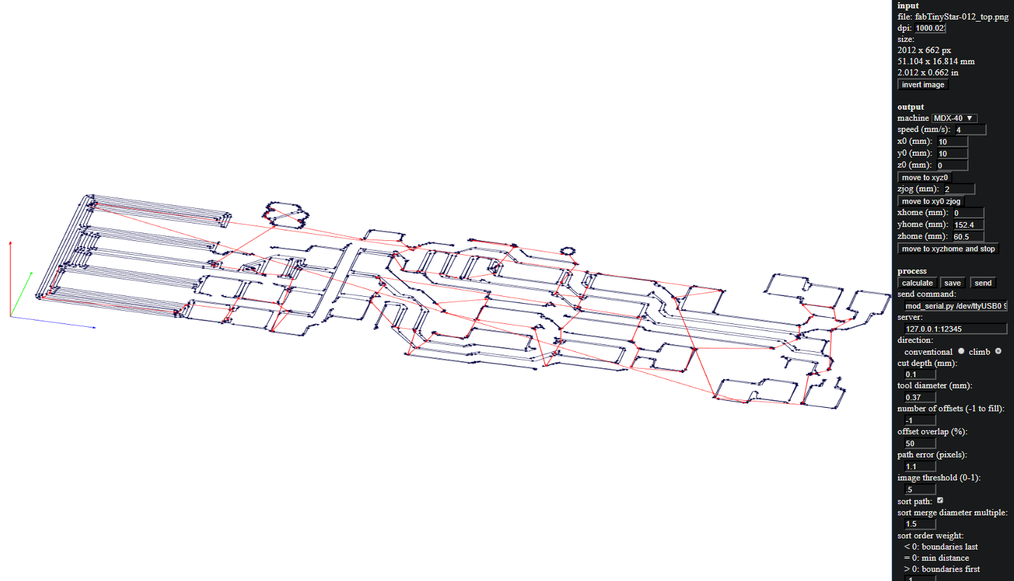
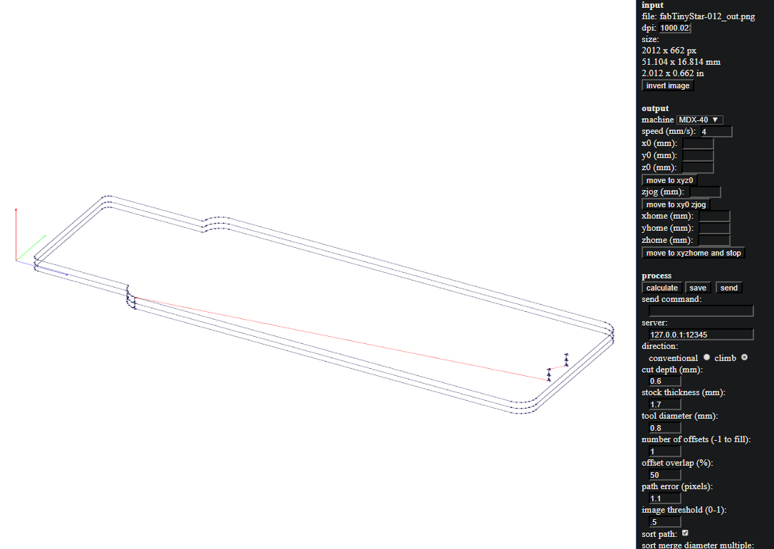
Press Calulate and once it has finished calculating the drillbit/endmill path, press Save. Now you can 3d view your pcb with different point of views using right and left click on the image, and use the mouse wheel to zoom in/out. Check if it’s everything ok by directly inspecting the image
-
Do the same procedure for Outline traces from step 1. To avoid buggy milling files, it’s better if you close the page and then open a new one and remember to not refresh the page or you will lose everything.
-
Then now we move the files in a usb key to transfer them to the CNC PC.
In summary the settings I used to mill the programmer are:
LET’S MILL THE BOARD!
Now that we have all rml ready for production:
-
We open the machine door and we clean the sacrifical layer.
-
We take the double sided tape and, after cleaning the surface of the sacrifical layer and the surface of the pcb that has to be sticked, we stick them together. This will ensure perfect sticking and no backlash due to vibrations of the milling process. Be sure to stick the board in the work area of the cnc, In this case the work area of the cnc is really visible.
-
We open the program called “Vpanel” on the cnc’s PC.
-
With dimension of the board in mind, we choose one point as you like and set that XY point as your origin. So move with the green and red arrows on the XY plane. then press to “SET” > “XY origin”
-
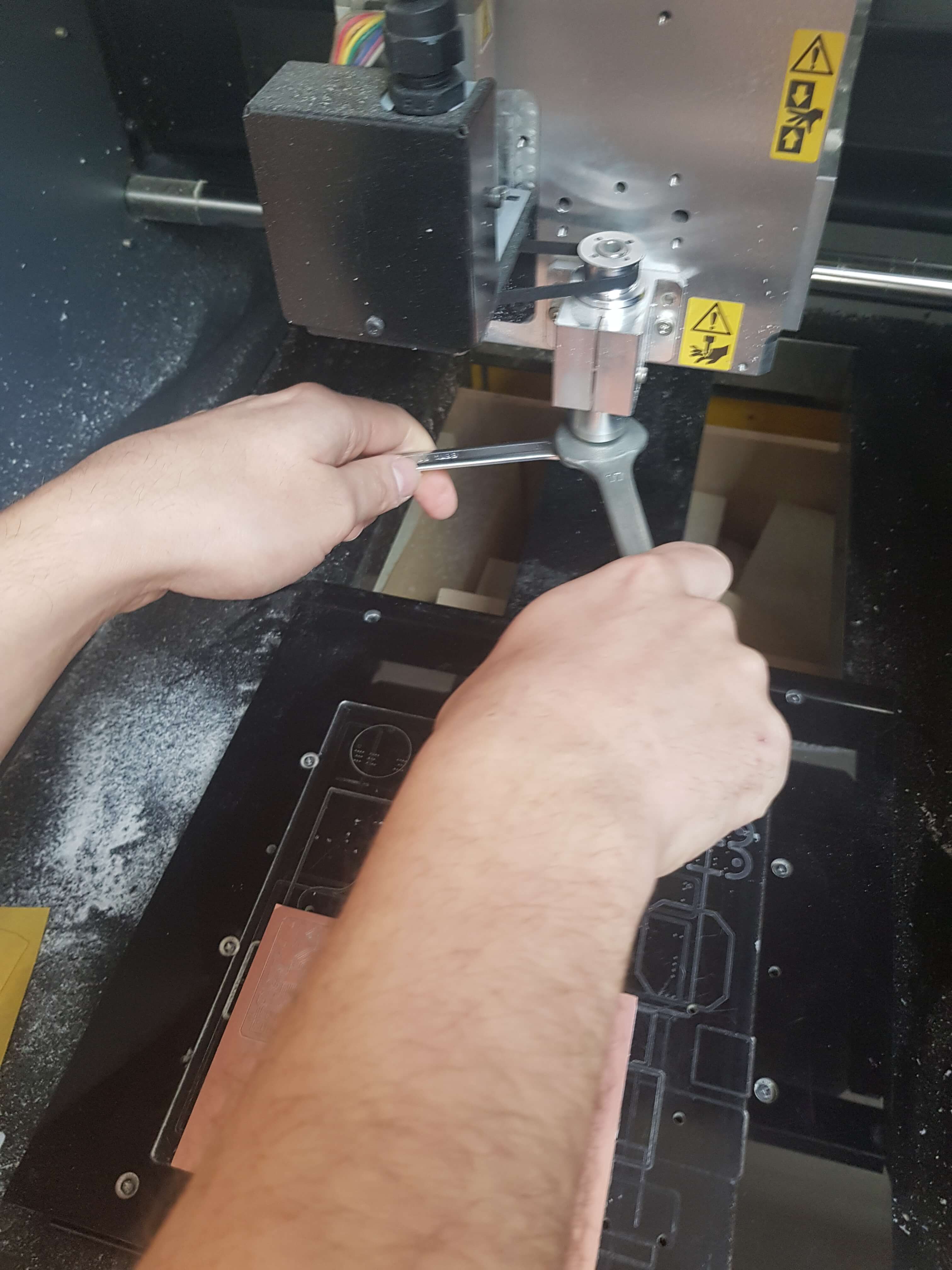
First of all we have to mill the traced of the board, so we take the V-shape 30° tool and the tighten with keys the tool to the spindle mechanism. Be careful to don’t overtight or you can damage the fillet.
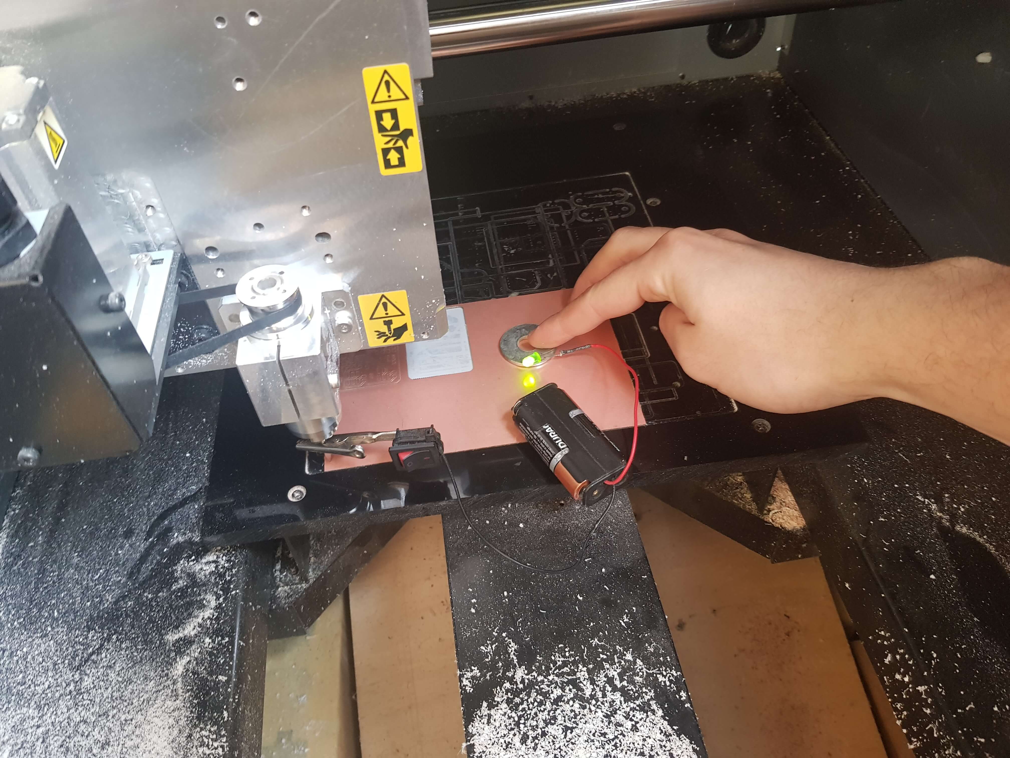
- To set the Z height properly, the edge of the mill has to barely touch the copper surface of the board. In order to know the right Z Height we have to use a small and easy to build circuit basically when the circuit is close that’s meaning that the the edge of the mill is touching in the right way and so the LED is ON. Move up and down with the Blue buttons on the Z axis. Then, on the right height, click on “SET” > “Z origin”.
## The Z probe Circuit
The circuit is built as a series of 1/2 batterys, a current limiting resistor, a LED, (an optional switch for battery life -saving) . They haven't to be in a specific order, remember the right polarity of the LED: the Anode has to be wired to the positive pole of the battery. At the edges of the circuit you have to solder a Washer and an Alligator clip! Yup, the circuit is done!
-
You can now move anywhere else and then click to “MOVE” > “XYZ origin” to verify if you did all step right.
-
Now you can start milling the traces: click on “CUT” and add the rml trace file you want. Then click on “OUTPUT” and the cnc will start milling.
-
During the milling, you can press the VIEW button in order to temporarily stop the machine to take a view of your work if something seems to go wrong. In emergency cases, press the RED BIG BUTTON to permenently stop the cnc working.
-
Once the trace’s milling has finished, repeat steps from step 6, but first remember to change your mill bit moving on the Z axis, in order to complete the outline of the board.
## Remember

DO NOT RESET the XY origin until you finish the board (traces + outline milling ): re-find your  old XY origin is nearly impossible, but you can try.
….
##Design rules characterizing
…
Choosing my programmer
Basically, you can adopt different protocols to program your microcontroller:
- SPI protocol
this method is used in the Arduino UNO board. Infact the main programmer is the ATMEGA16U4 that programs the real microcontroller you are using (yes, the programmer is still a microcontroller). From here I discovered that the ATMEGA-U-SERIES support the direct usb protocol. In that way the arduino board doesn’t require a ftdi chip (maybe it’s a convenient choice from a commercial point of view).
- Uart/Usart protocol
this is the method used when you’re dealing with FTDI chips(to name some of the most famous of them: FTDI232RL,FT230X,FT231X). Whenever you see pins like TX(transmit),RX(receive),CTS(Clear to Send),VCC(common collector voltage/supply voltage),GND(ground),DTR(Data terminal ready) it’s sure you’re operating with uart/usart.
-Advantages: easy to plug in usb port of your computer, doesn’t requires to program the chip (you don’t have to flash a bootloader on it)
-Drawbacks: slow baud rate and you’ve to take care of the boot configuration of the chip everytime. By the way if your ftdi chip has the DTR pin the process of uploading the program is automatic.
- UPDI
This interface is used to program microcontrollers with only 2 pins. This is a proprietary interface for the new Attiny and AVR, so choose this method only if you’re willing to program only with this devices. I was so fascinated about UPDI programmer(because I’ve nevere heard about it) but the main drawback I encountered in the fab USB-UPDI programmer is that the sharing of the supply voltage with the target pcb is missing. This is a cool feature and I think it’s very convenient to have in a programmer board.
Anyway, I noticed that a standard updi connection has not yet been defined even if Someone tried to design in.
Another thing I learned is that serial monitor debug over UPDI is allowed only if an official ATMEL IDE is used.
To program with updi you have to program the chip with jtag2updi by SpenceKonde, you can check it out a tutorial here. He’s is using an arduino nano instead of an ATMEL ICE.
Fabtiny*
My choice is that programmer.
First of all I think is well documented, it has more than one features (wow, I didn’t expected a programmer has also a tv-b gone feature…), and I like that the designer took care about the usb overcurrent protection (this is a really good thing for our poor usb port, remember if you will burn it you have to change motheboard of you pc, sometimes). It’s also compatible with newer ATtiny chips.
There are board based on building difficulty, so you can choose the one you want, build it many times with different layout and precautions. That’s cool. Personally I choose the easiest way, the BAS version.
Here’s the tutorial for programming the this board.
Extracting the BOM (Bill of Material)
In order to don’t be confused about the component you’re going to solder, open the schematic of the board with Eagle and click on ULP> “bom.ulp” to generate your BOM. I choose the txt format. Here’s the BOM:
Part Value        Device                    Package       Description
C1   10uF         UNPOLARIZED_CAPACITOR1206 1206          unpolarized_capacitor
C2   100nF        UNPOLARIZED_CAPACITOR1206 1206          unpolarized_capacitor
D1   3v3          ZENER_DIODESOD123         SOD123        zener diode
D2   3v3          ZENER_DIODESOD123         SOD123        zener diode
IC1  ATTINY*5     ATTINY45SI                SOIC8
JP1  PINHD-2X04   PINHD-2X04                54202-G0808LF
LED1 red          LEDSMT1206                1206          LED
LED2 green        LEDSMT1206                1206          LED
R1   1K           RESISTOR1206              1206
R2   49           RESISTOR1206              1206
R3   49           RESISTOR1206              1206
R4   49           RESISTOR1206              1206
R5   1K           RESISTOR1206              1206
R6   499          RESISTOR1206              1206
R7   ptc          RESISTOR1206              1206
S1   SLIDE-SWITCH SLIDE-SWITCH              AYZ0102AGRLC
S2                6MM_SWITCH6MM_SWITCH      6MM_SWITCH    OMRON SWITCH
USB  USBPCB       USBPCB                    USB-A-PCB     USB Connectors
Example title
In order to install the WSL you have to: hello