Electronics Design 📋
🕘 Date / Time:
Hello there..^^. Hope a large smile finds its way to your face ^^. Everything is awesome on the sixth week of Fab Academy.. ^^ We had a group assignment and Individual assignment just like last week. ^^
___________________________________________
A) Group Assignment:
This week's assignment was to use the test equipment in our lab to observe the operation of a microcontroller circuit board.
___________________________________________
B) Individual Assignment:
My assignment for this week is to redraw an echo hello world board adding at leats an LED and a button and program that circuit using the ISP.
Echo circuit hardware:
For the redrawing and PCB design I used Eagle CAD.I chose to use it because I had an previous experience with it _little as it was but still it was there once_, and there is a "fab library" for almost all the components we're going to use in the academy.
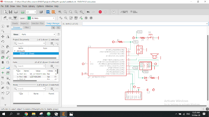
My first idea of a functioning circuit, was one that has music in it, user pushes a button, an LED is lit and a tune is played. So, I tried to make that work.
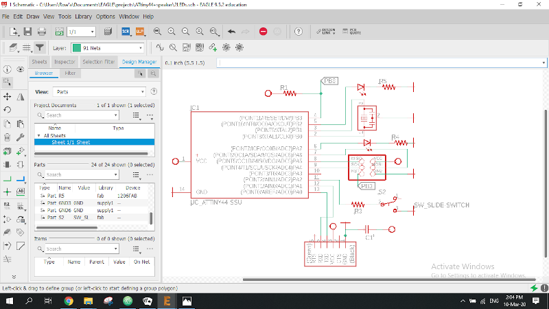
A) Circuit Schematic Diagram:
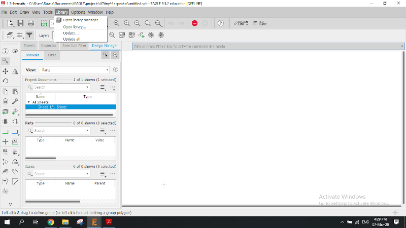
1- I downloaded "Fab library"
here and put it in the equivilant of "C:\Users\Row'a\Documents\EAGLE\libraries" on your laptop :D.
2- I opened eagle, created a new project, a new schematic and started adding parts.
3- I loaded the library into Eagle.
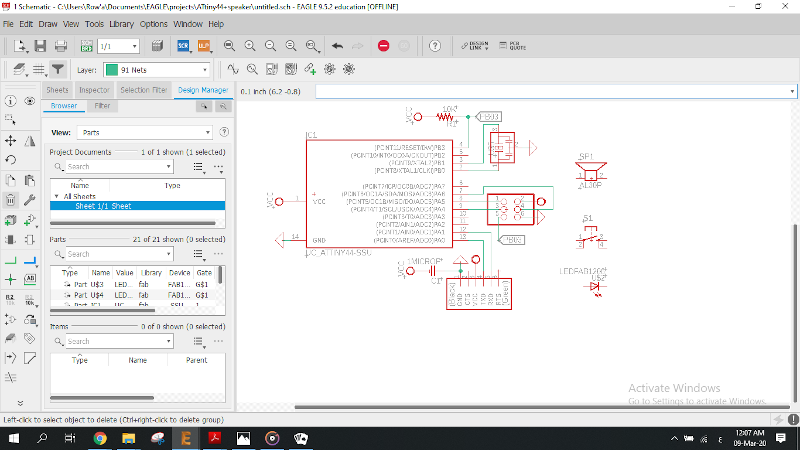
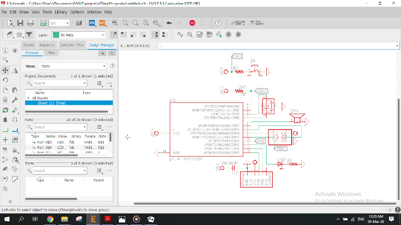
4- I drew the main circuit first.
5- Then added the extra components.
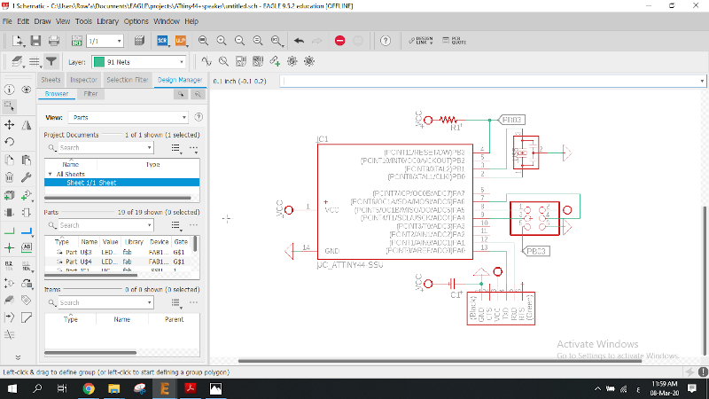
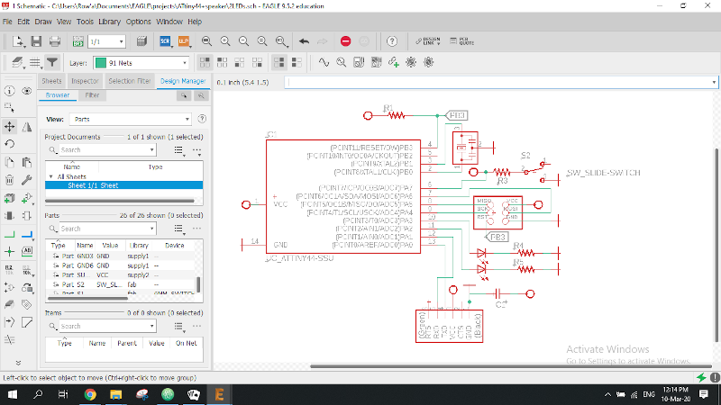
After that step, the computer shuts down, the schematic was not saved and I had to redraw it. Then I decided to change the push button to a slide switch and cancelled the speaker as the actual components were too large to put on my circuit in mind.
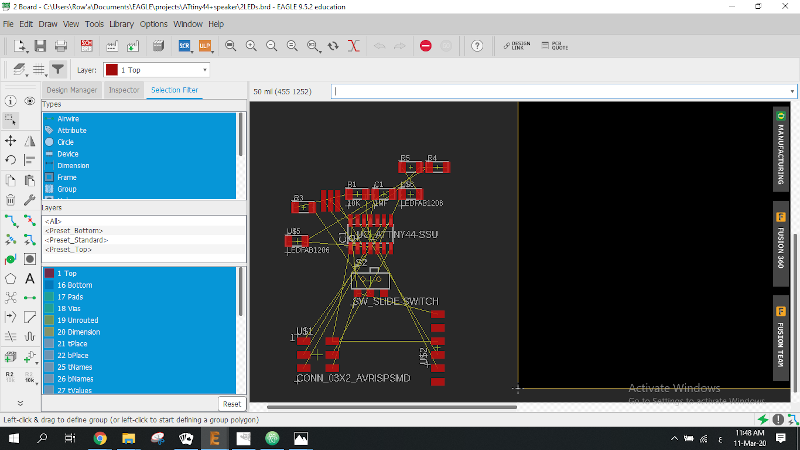
Then it was time to do the routing. Because it was my first time designing a PCB on Eagle CAD, I thought "Auto Routing" was the thing people usually use to get the routing done.
So I tried it several times and the closest I was to an appropiate routing was 86%.
I consulted a college, did some research and found out that auto routing is in fact the least recommended method and that it's preferable for the PCB maker to design his own routing.
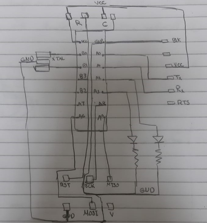
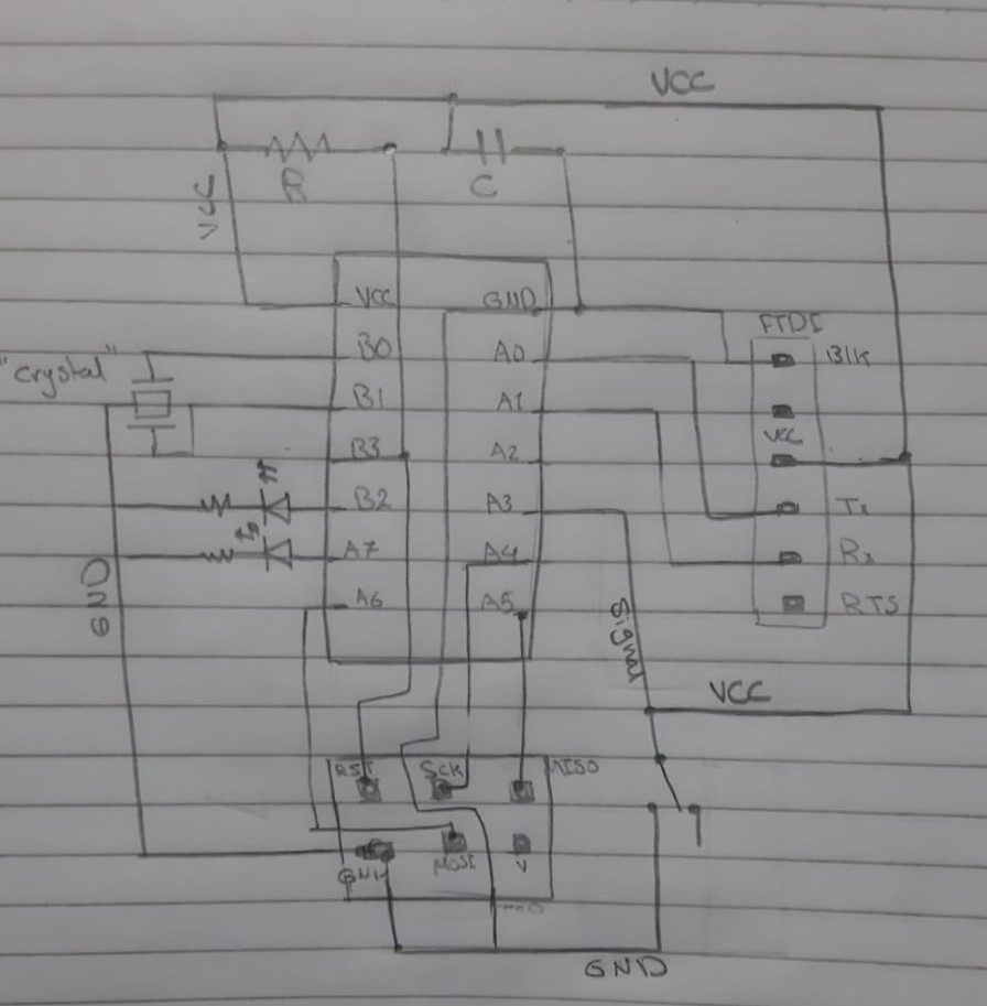
I drew a free hand manual routing sketch in order to arrange my added components and be able to connect them properly. It was easier to start from the original PCB.
Putting some thinking into it I figured out that I'll have to change the LEDs from pins (A2 & A3) to pins (A7 & B2) as they only need signal and ground yet the slide switch needs signal, VCC and ground so that I moved it to pin A2 to be able to reach a ground and VCC.
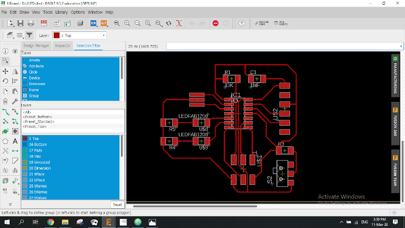
B) PCB Design:
And now that I have my schematic all done, it's time my first CAD PCB ever ^^.
1- Clicked on "generate / switch to board".
2- There I found all of my components scrambled together on the left and the connections between them are in the form of air wires.
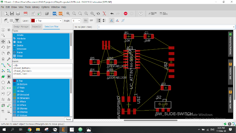
3- I started organizing them in places just like the sketch I drew.
4- Rotated some of the components to match the sketch and to have minimum air wires crossings.
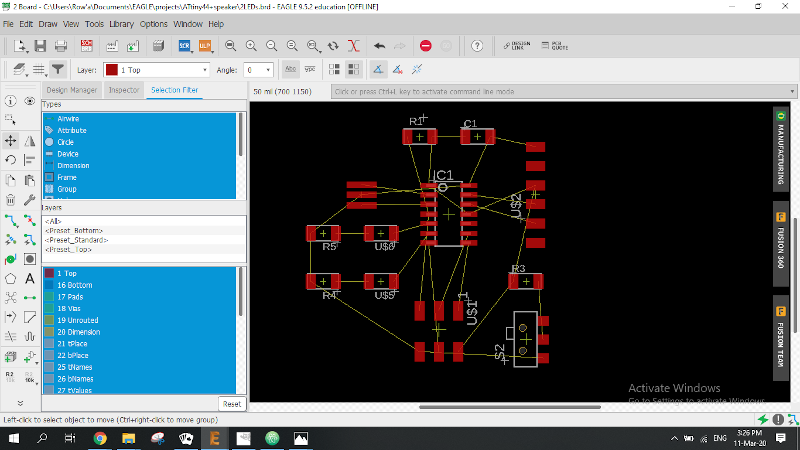
5- Did the routing, did the Design Rule Check AKA "DRC" and all was well.
6- Turned off all layers except for the Top layer with the traces.
7- Zoomed in my PCB so that it could fit the window, exported the traces as Image (Monochrome, 500 dpi, Window) then Ok. ^^

C) Creating PCB Outline:
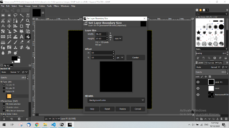
Steps for creating an outline usin Gimp:
1- Open the PCB image with Gimp.
2- From "layer" menu, add a new layer in white (The same size of the PCB image).
3- From "Layer" menu add another layer but in black.
4- While selecting the black layer, get to "Layer" menu then select "Layer Boundary Size".
5- Change "Layer Size" into millimeters.
6- Increase width and height each by 2 mm.
7- Then Press "Center" then "Resize".
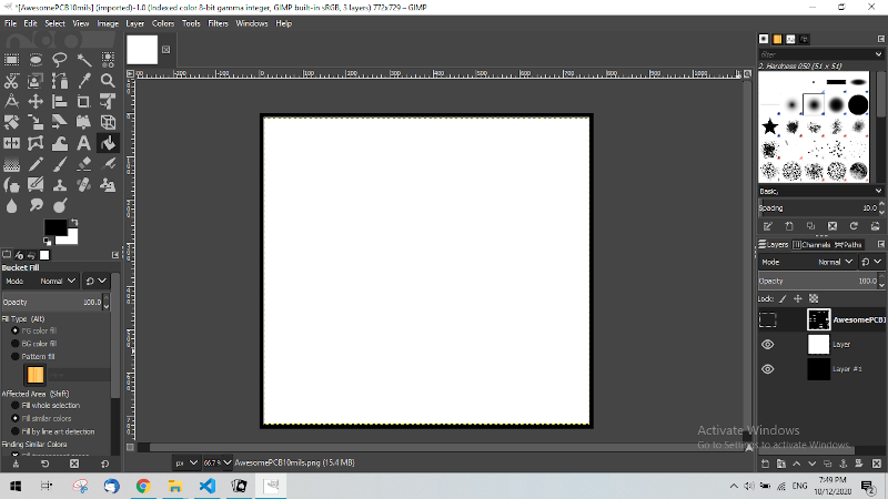
Doing that we would have 3 layers of images, make sure they are put in order the small white one 1st then the black then you can hide the pcb itself or put it last. then save that image as png to then use it in "fab modules".
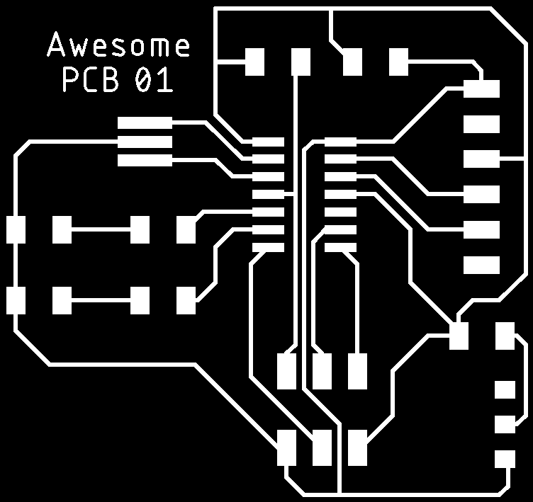

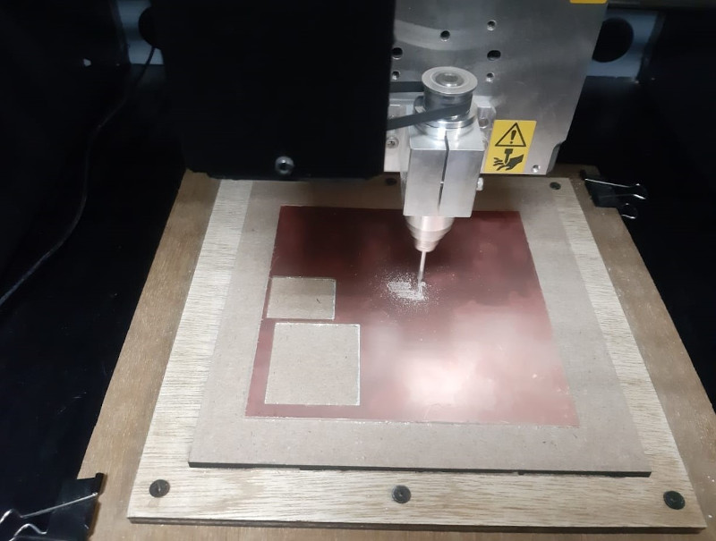
D) Manufacturing:
Having the PCB traces and outline it was time for fab moduleas an that was illustrated in details in electronics production week.
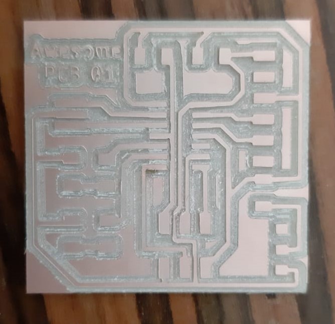
D) Soldering:
After milling my lovely PCB the only thing left was to solder my SMD components on it then give programming a try a week from now on embedded programming.
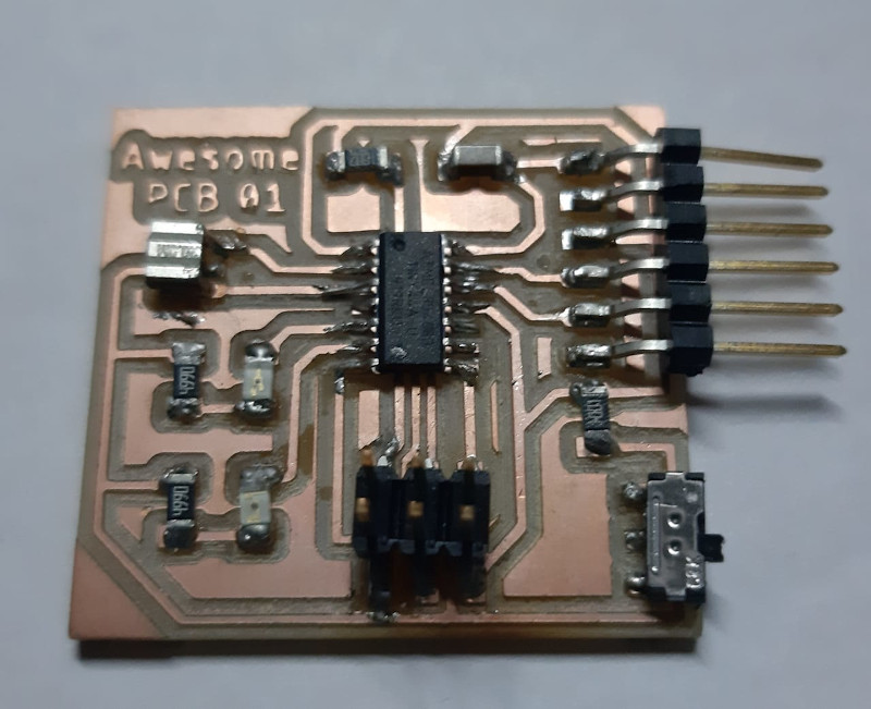
Note: that I discovered later on (on embedded programming week) that the slider switch is connected in a wrong way and I won't use it.
E) Testing code:
  const int Red = 7;

  void setup(){
            pinMode(Red, OUTPUT);
  }

  void loop() {
  //Get Ready
            digitalWrite(Red, HIGH);
            delay(3000);
            digitalWrite(Red, LOW);
            delay(3000);

        //B
             digitalWrite(Red, HIGH);
            delay(750);
             digitalWrite(Red, LOW);
            delay(250);

            digitalWrite(Red, HIGH);
            delay(250);
            digitalWrite(Red, LOW);
            delay(250);

            digitalWrite(Red, HIGH);
            delay(250);
            digitalWrite(Red, LOW);
            delay(250);

            digitalWrite(Red, HIGH);
            delay(250);
            digitalWrite(Red, LOW);
            delay(750);

        //Y
            digitalWrite(Red, HIGH);
            delay(750);
            digitalWrite(Red, LOW);
            delay(250);

            digitalWrite(Red, HIGH);
            delay(250);
            digitalWrite(Red, LOW);
            delay(250);

            digitalWrite(Red, HIGH);
            delay(750);
            digitalWrite(Red, LOW);
            delay(250);

            digitalWrite(Red, HIGH);
            delay(750);
            digitalWrite(Red, LOW);
            delay(750);


        //E
           digitalWrite(Red, HIGH);
           delay(250);
           digitalWrite(Red, LOW);
           delay(250);

           digitalWrite(Red, HIGH);
           delay(250);
           digitalWrite(Red, LOW);
           delay(1750);


      //R
            digitalWrite(Red, HIGH);
            delay(250);
            digitalWrite(Red, LOW);
            delay(250);

            digitalWrite(Red, HIGH);
            delay(750);
            digitalWrite(Red, LOW);
            delay(250);

            digitalWrite(Red, HIGH);
            delay(250);
            digitalWrite(Red, LOW);
            delay(750);

        //O
            digitalWrite(Red, HIGH);
            delay(750);
            digitalWrite(Red, LOW);
            delay(250);
            digitalWrite(Red, HIGH);
            delay(750);
            digitalWrite(Red, LOW);
            delay(250);
            digitalWrite(Red, HIGH);
            delay(750);
            digitalWrite(Red, LOW);
            delay(750);

        //W
            digitalWrite(Red, HIGH);
            delay(250);
            digitalWrite(Red, LOW);
            delay(250);

            digitalWrite(Red, HIGH);
            delay(750);
            digitalWrite(Red, LOW);
            delay(250);

            digitalWrite(Red, HIGH);
            delay(750);
            digitalWrite(Red, LOW);
            delay(750);

        //A
            digitalWrite(Red, HIGH);
            delay(250);
            digitalWrite(Red, LOW);
            delay(250);

            digitalWrite(Red, HIGH);
            delay(750);
            digitalWrite(Red, LOW);
            delay(750);
   }
___________________________________________
Downloadables: 💾
©️ Row'a M. M. Othman - Fab Academy 2020