Week 8- Embedded Programming
Overview
For this week we have two assignments:
- Group assignment
- Individual assignment
Compare the performance and development workflows for different microcontroller families
Read the datasheet for the microcontroller you are programming. Program the board you have made to do something, with as many different programming languages and programming environments as possible.
My Assignment Steps:
Step (1): Read and explain Attiny45 datasheet
Step (2): Program my board
The Process
Read and Explain Attiny45-Datasheet
Datasheet is an instruction manuals for the electronic component. It explains exactly what a component does and how to use it. Unfortunately these documents are usually written by engineers for other engineers, and as such they can often be difficult to read. So, you can start from this Tutorial that explain how to read datasheet in a simple way.
I start by download Attiny45 Datasheet and Summary datasheet as I know for this assignment I only need to know:
I read the summary datasheet and here what I came up with regarding to the above points
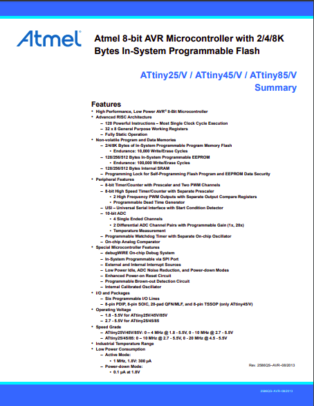
Attiny45-Featutures:
1-Attiny45 is an 8bit-microcontroller: which mean it has 8 buses to carry on the data in another word it can transfer 2^8=256 instructions per cycle.
2-Program Memory: 4k bytes Flash memory, (In System Self-programmable" simply means the microcontroller can update its own flash while running)
3-Data memory: 256 bytes EEPROM memory and 256 bytes SRAM.
4-I/O port: 8 pins with six of them working as programable I/O lines
5-Operating Voltage 1.8 : 5.5V for ATtiny25V/45V/85V // 2.7 - 5.5V for ATtiny25/45/85.
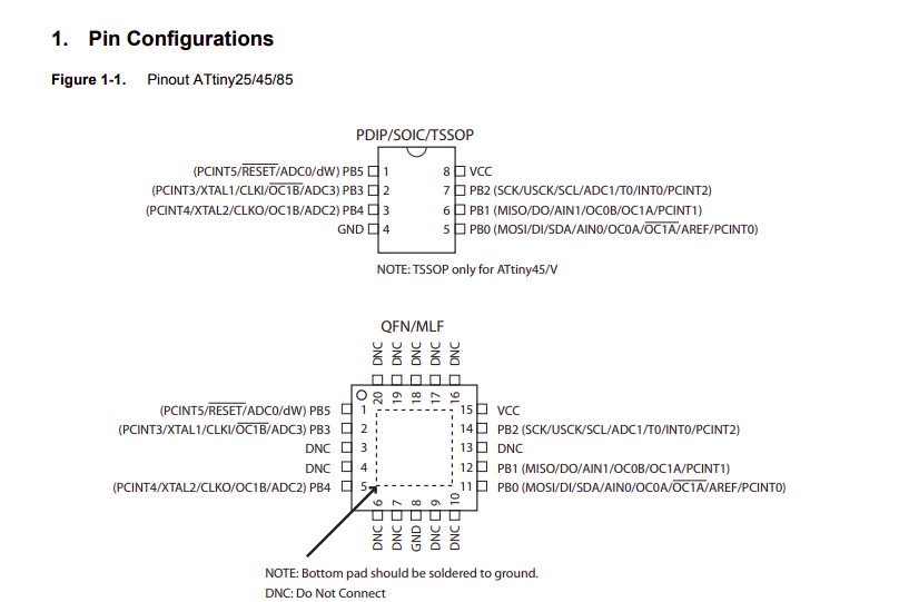
Pinout and Pin description
The Pin description are what you need when you program the board to know how to address and control them using C language. Attiny45 has one type of I/O port :Port B is a 6-bit bi-directional I/O port with internal pull-up resistors (selected for each bit).
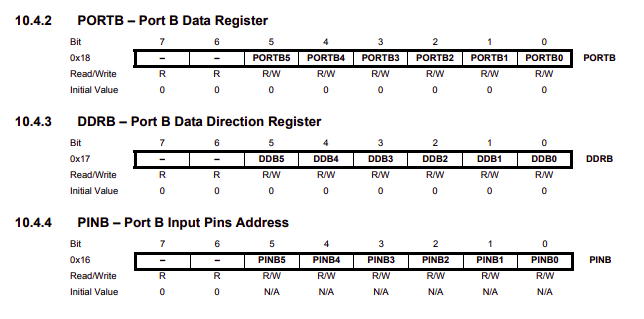
GPIO Registers:
In order to use port-B as I/O we need to understand the I/O register of the port:
DDRB: Data Direction 8 bit registers
PORTB: Data 8 bit registers
PINB: Input Pins 8 bit registers
Programming The Board
A quick reminder about the board
In Electronic design week I create and test an Attiny45 based board that have one Input and two outputs:
- One Input "switch" -> PIN2 - from datasheet I know it is PB3.
- A Power Led that turn on once the power is connected to the board.
- A Programmable led -> PIN3 from datasheet I know it is PB4 that we control the output depend on the state of the switch.
for this week I decided to write the code in C and using Arduino IDE.
Workflows
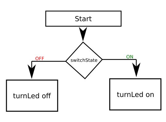
1- I draw a simple flowchart to visualize my steps and how is the program gonna work before start coding
2- From datasheet I know which register I need to configure DDRB, PORTB, PINB
3- From my design I know which pin exactly will be the input PB3. and which pin will be the output PB4.
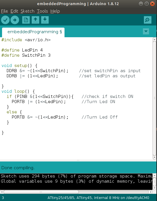
 #include < avr/io.h >
 #define LedPin 4
 #define SwitchPin 3

 void setup() {
   DDRB &= ~(1<< SwitchPin);    //set switchPin as input
   DDRB |= (1<< LedPin);        //set ledPin as output
 }
 void loop() {
   if (PINB &(1<< SwitchPin)){   //check if switch ON
 	 PORTB |= (1<< LedPin);      //Turn Led ON
   }
   else {
	 PORTB &= ~(1<< LedPin);     //Turn Led Off
   }
 }
Upload the code
we will going to upload the code to our board using arduino IDE and using arduino as our programmer as we did in Electronics production week
1- Install Attiny library support for Arduino IDE
https://raw.githubusercontent.com/damellis/attiny/ide-1.6.x-boards-manager/package_damellis_attiny_index.json
2- Prepare the arduino Board as a programmer
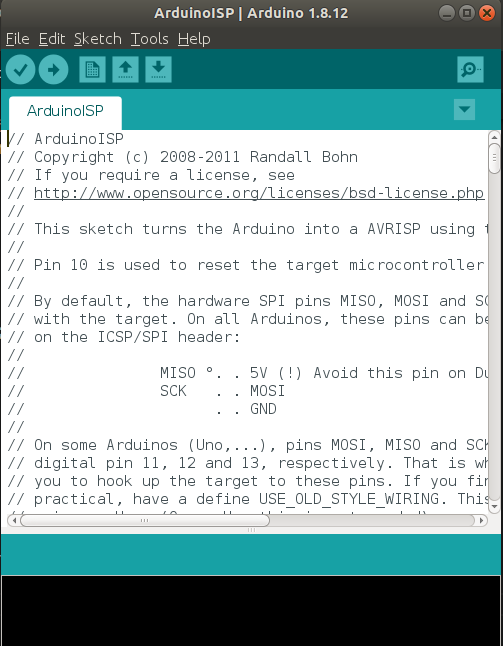
3- Upload the Bootloader
slave reset: 10
MOSI:        11
MISO:        12
SCK:         13
4- Upload the Code
Group Assignment
Internal Architecture
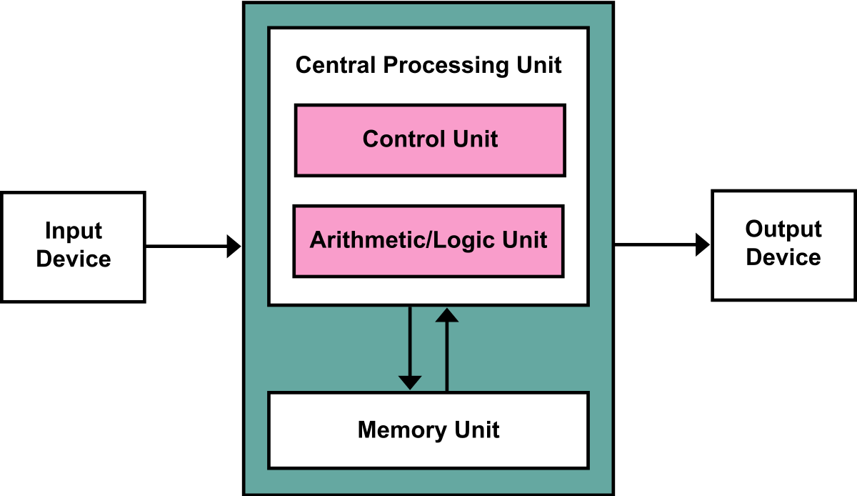
All MCs use one of two basic design models: Harvard Architecture and von-Neumann architecture. They represent two different ways of exchanging data between CPU and memory.
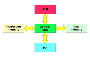 Harvard_architecture
 Von_Neumann_Architecture
- MCs with Harvard architecture are called "RISC MCs".
- MCs with vonNeumann's architecture are called 'CISC MCs'.
- Harvard architecture is a newer concept than von-Neumann's.
- In Harvard architecture, data bus and address bus are separate. Thus a greater flow of data is possible through the CPU, and a greater speed of work.
- Harvard architecture have fewer instructions than von-Neumann's, and the instructions usually executed in one cycle.
Difference between AVR and ARM
A micro-controller is a single Integrated Circuit (IC) which is comparable to a little stand alone computer and it is designed to perform the specific tasks of embedded systems.
AVR micro-controller is manufactured by Atmel corporation in the year 1996. It is based on RISC Instruction set Architecture (ISA) and also called as Advanced Virtual RISC.
ARM micro-controller was introduced by Acron computer organization and is manufactured by Apple, Nvidia, Qualcomm, Motorola, ST Microelectronics, Samsung Electronics, and TI etc. It is based on RISC Instruction set Architecture (ISA) and also called as Advanced RISC Micro-controller.
| # | AVR | ARM |
|---|---|---|
| 1 | It has bus width of 8 bit, 16 bit and 32 bit. | It has bus width of 32 bit and also available in 64 bit. |
| 2 | It uses ART, USART, SPI, I2C communication protocol. | It uses SPI, CAN, Ethernet, I2S, DSP, SAI, UART, USART communication protocol.1 clock per instruction cycle. |
| 3 | 1 clock per instruction cycle. | 1 clock per instruction cycle. |
| 4 | Its family includes Tiny, Atmega, Xmega, special purpose AVR. | Its family includes ARMv4, 5, 6, 7 and series. |
| 4 | Flash, SRAM, EEPROM memory. | Flash, SDRAM, EEPROM memory.. |
Workflows for AVR microcontrollers tinyAVR series
In this week I document my workflows using Attiny45 as my main microcontroller.
Workflows for AVR microcontrollers megaAVR series
In Input devices week and Output devices week I document my work using arduino Atmega328 as my Pandemic version of the individual assignment due to covid-19.