Project
Final Project
Input devices and In-out board(week 9 + α)
Requirement
For changing a tempo, key, or sound set of musical sequencer, I want to add:
- Potentiometer
- 1: Interval of music (and the mosaic rate of capturered image)
- 2: Key change (adjust MIDI note number?)
- 3: Velocity range (the strength of play)
- 4: Duration (the length of 1 note)
- 5: Modulation (bibrat etc.)
- 6: (reserve)
- Tactile switch
- 1: Program change (Up)
- 2: Program change (Down)
- 3: Rhythm button(?)
- 4: (reserve)
For visualizing some of like interval(potentiometer 1) or program change(switch 1, 2), I want to embed a small OLED display (it will be added as one of output device). OLED display allow us to debug post launched project.
Devices
Checking usability, price and easiness of implementation, I decided to use following devices.
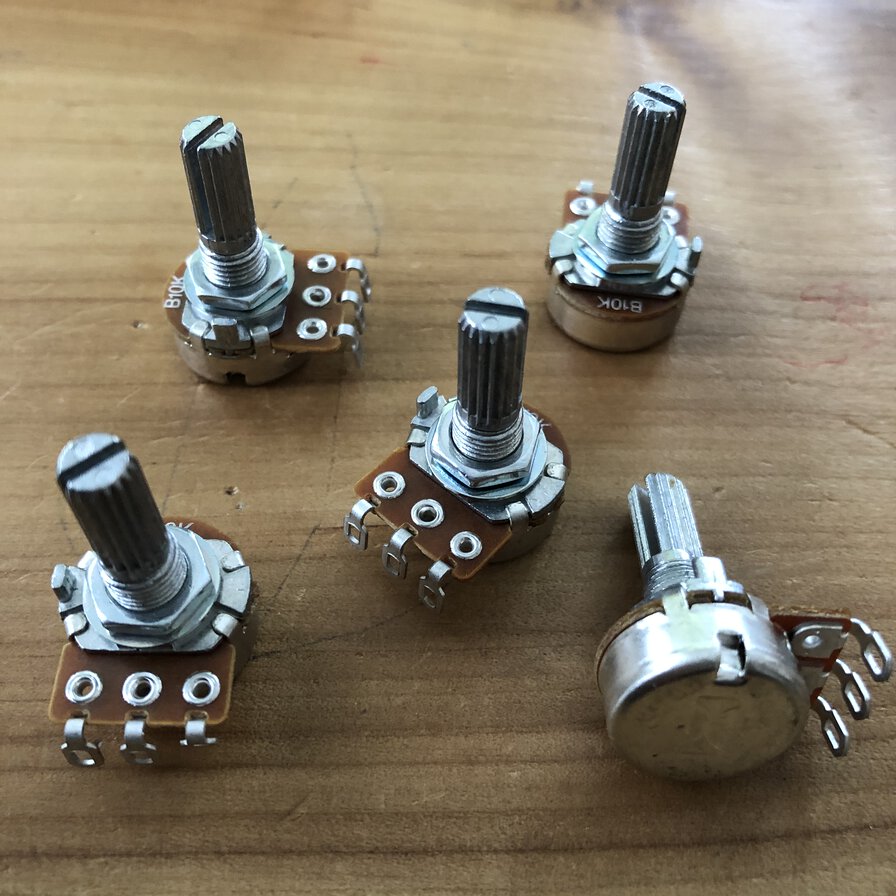
- Maker: Supertech Electronic Co., Ltd.
- Total resistance: 100~2MΩ
- Rated power(W): 0.125W
- Max. operating voltage: 200V
- Shaft: Φ6mm(screw M7), length 13.5mm
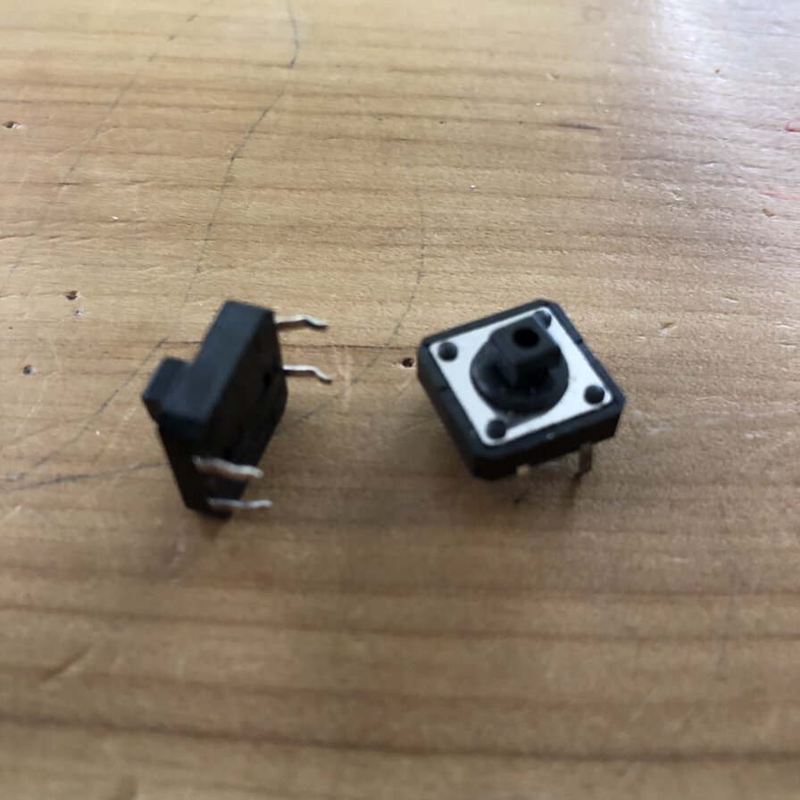
- Zhejiang Jianfu Electronics Co., Ltd
- Switching voltage:1~12VDC
- Switching current:1μA~50mA
- Resistance:under 100mΩ
- # of pins: 4
Input board
In week9 assignment, I defined my input devices for final project that enable to operate potentiometers and switches.
Actually, it's not completed as of 21 APril - I need:
- To setup the minimum path size for 16 mil in DRC rule.
- To separate a board for cabling potentiometers and the other board for attaching tact switches
- To identify the devices for final project especially in potentiometers.
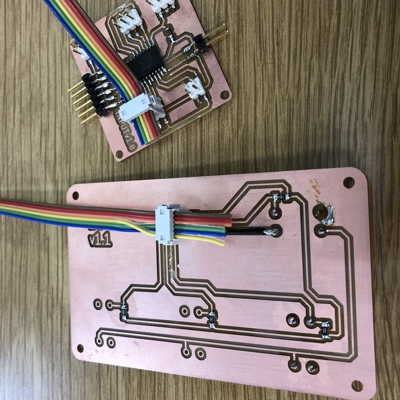
Input board as of 6 June (after coming back to lab from 2 months away by COVID-19)
After experiment in output device week, I decided to separate the input board and output board in different boards for modularity of system and performance (Multiple LEDs attached in NeoPixel takes time and microcontroller waits for finishing sequential blinking. It would be better for controller at output board to concentrate on output process without preventint input process. )
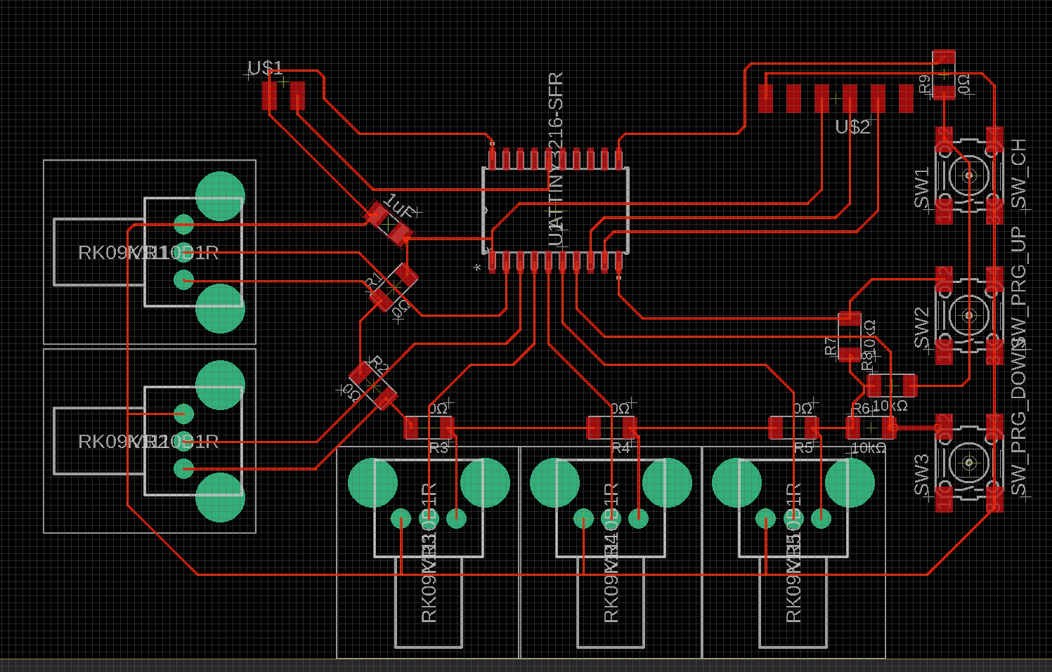
I re-desingned input board, mill it and tested it.
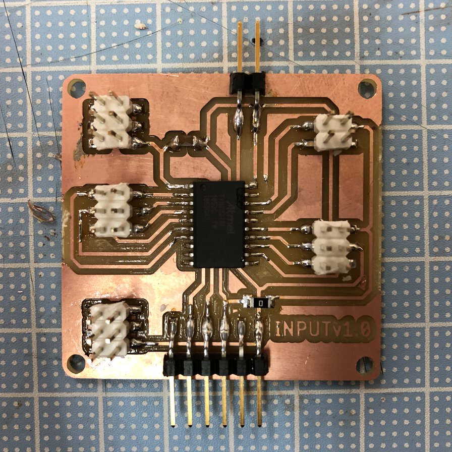
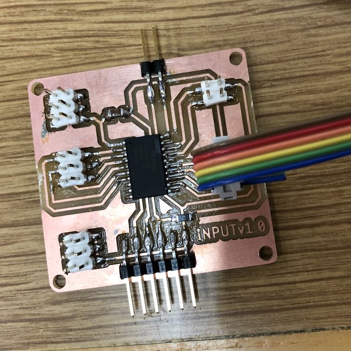
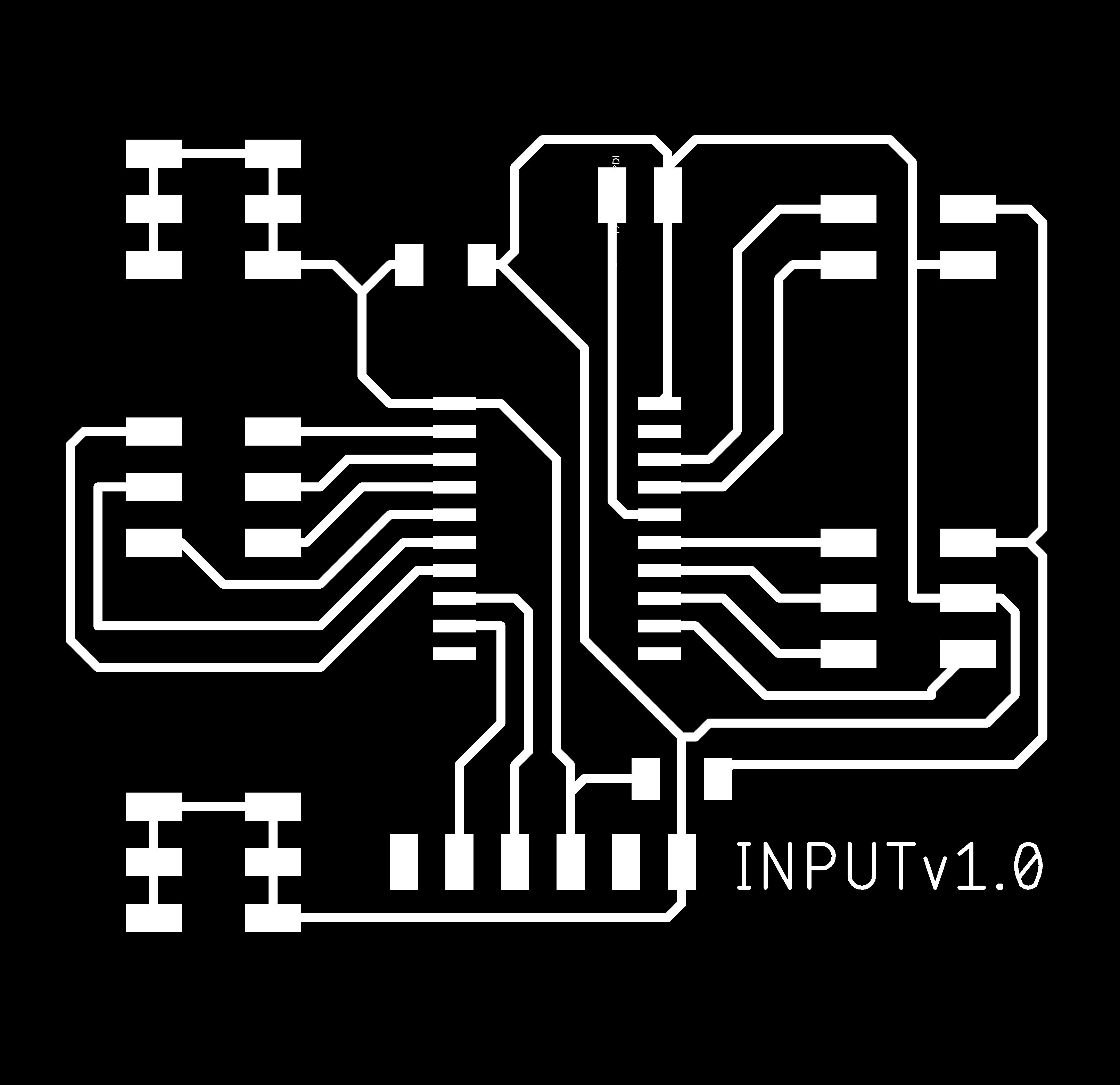
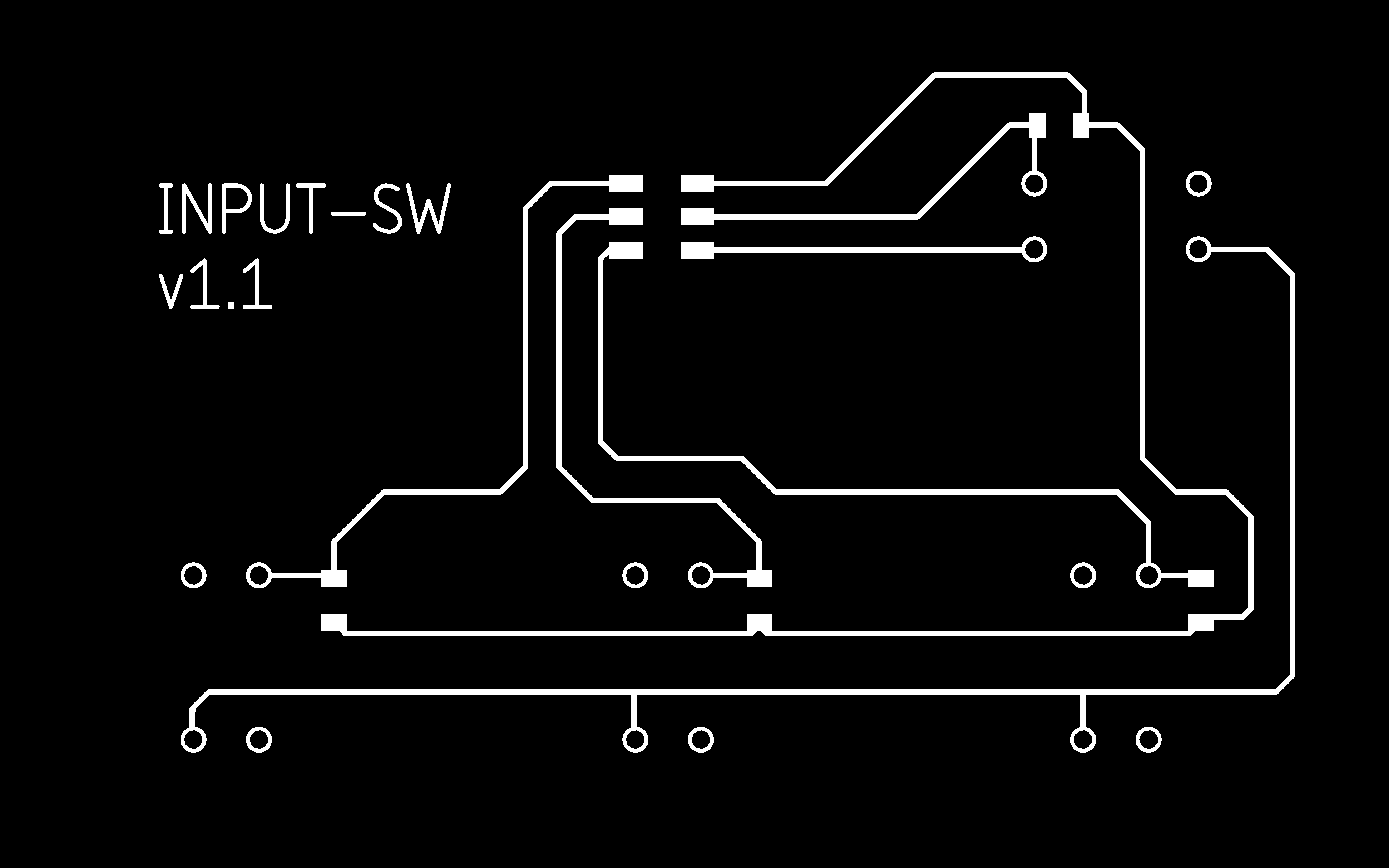
Input board v1.0
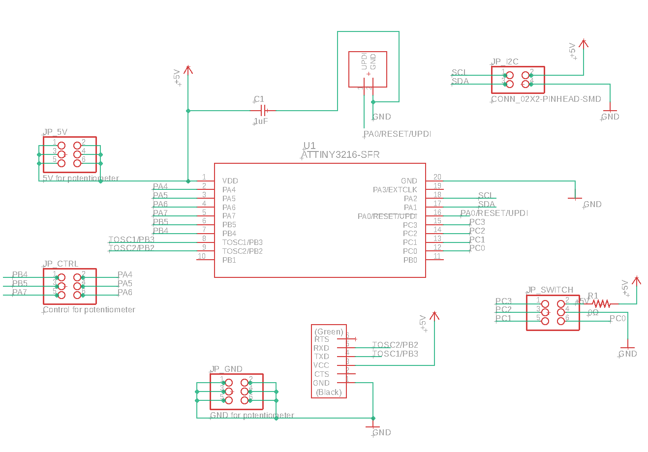
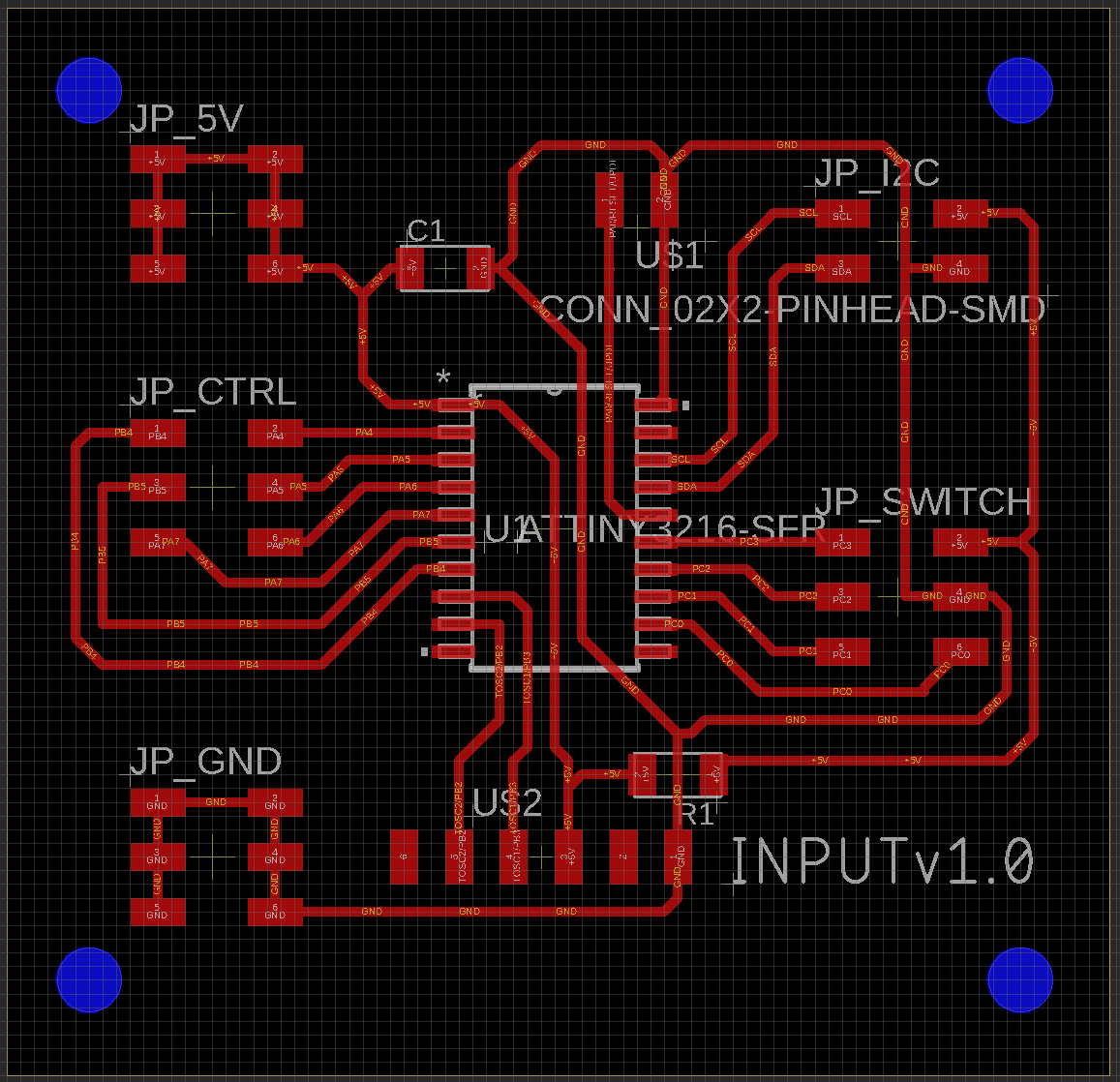
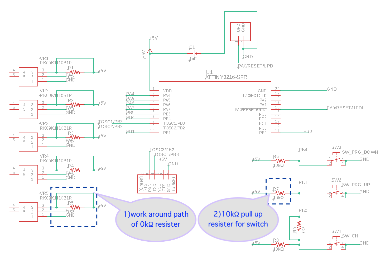
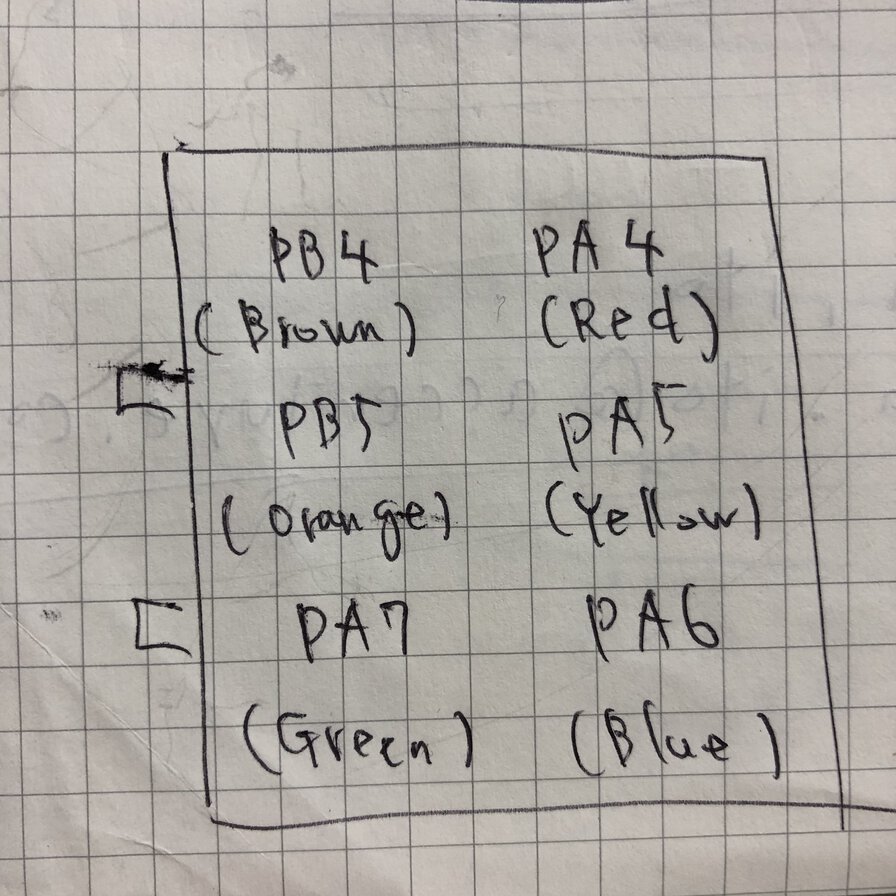
For attaching 5 potentiometers by PB4, PB5, PA7, PA4, PA5 and PA6("JP_CTRL"), VCC("JP_5V") and ground("JP_GND"), I added 3x2 pin headers to the board.
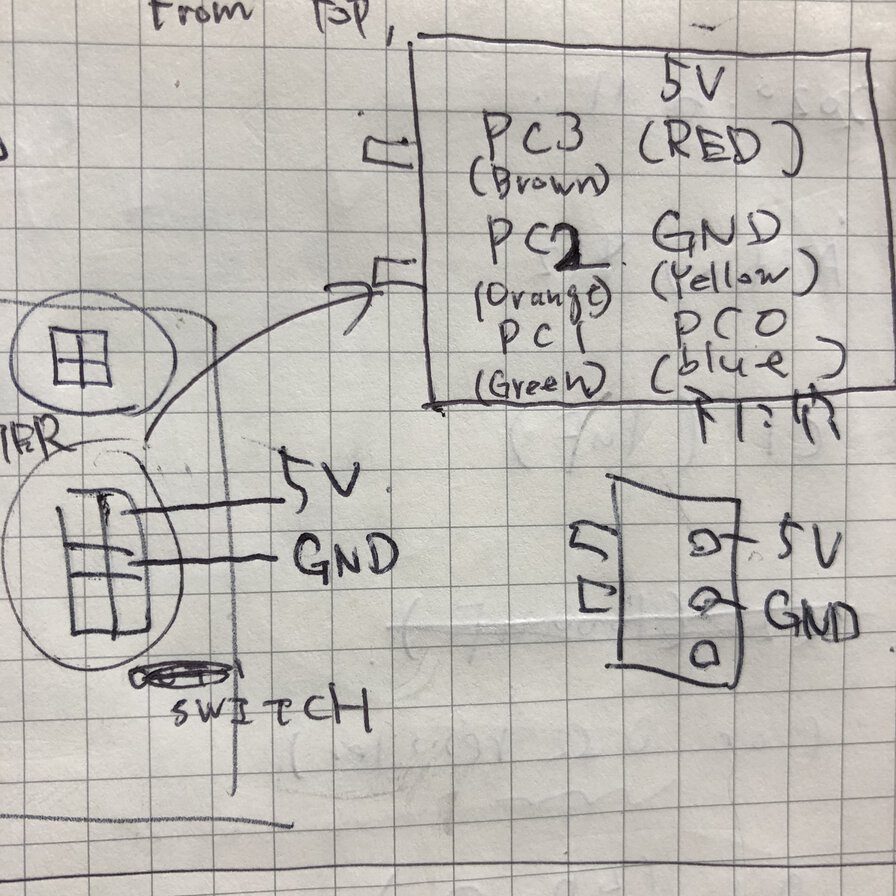
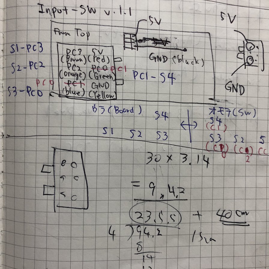
For connecting to other input board embedding tact switches, I use PC0, PC1, PC2, PC3 pins , VCC and Ground pin by 2x2 pin header ("JP_SWITCH")
For communicating with output board, I use I2C pins (SCL, SDA), VCC and Ground pin by 2x2 pin header ("JP_I2C")
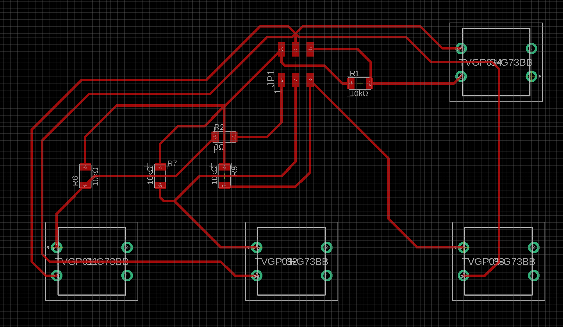
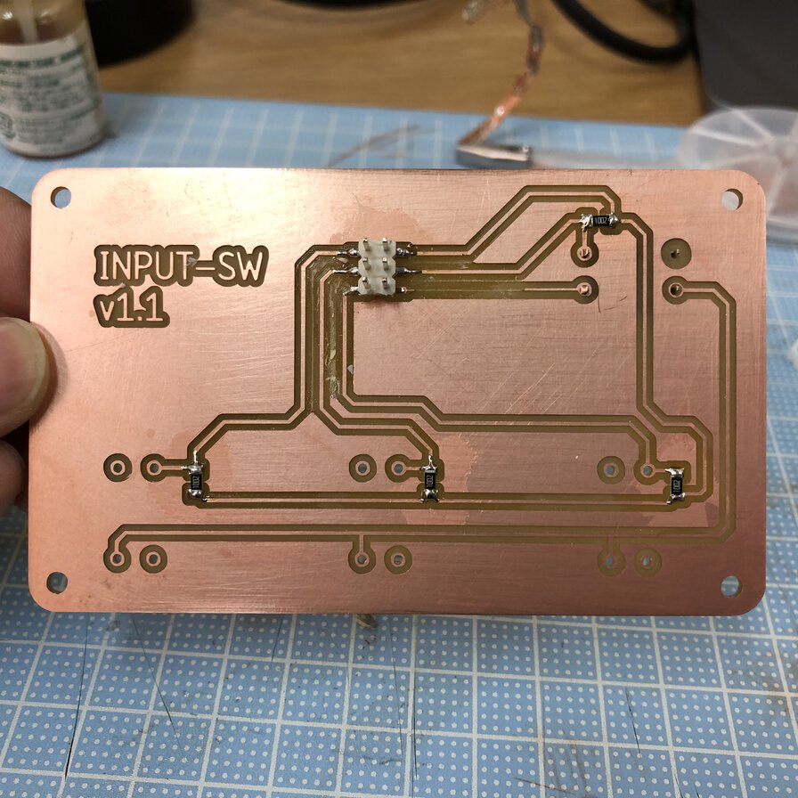
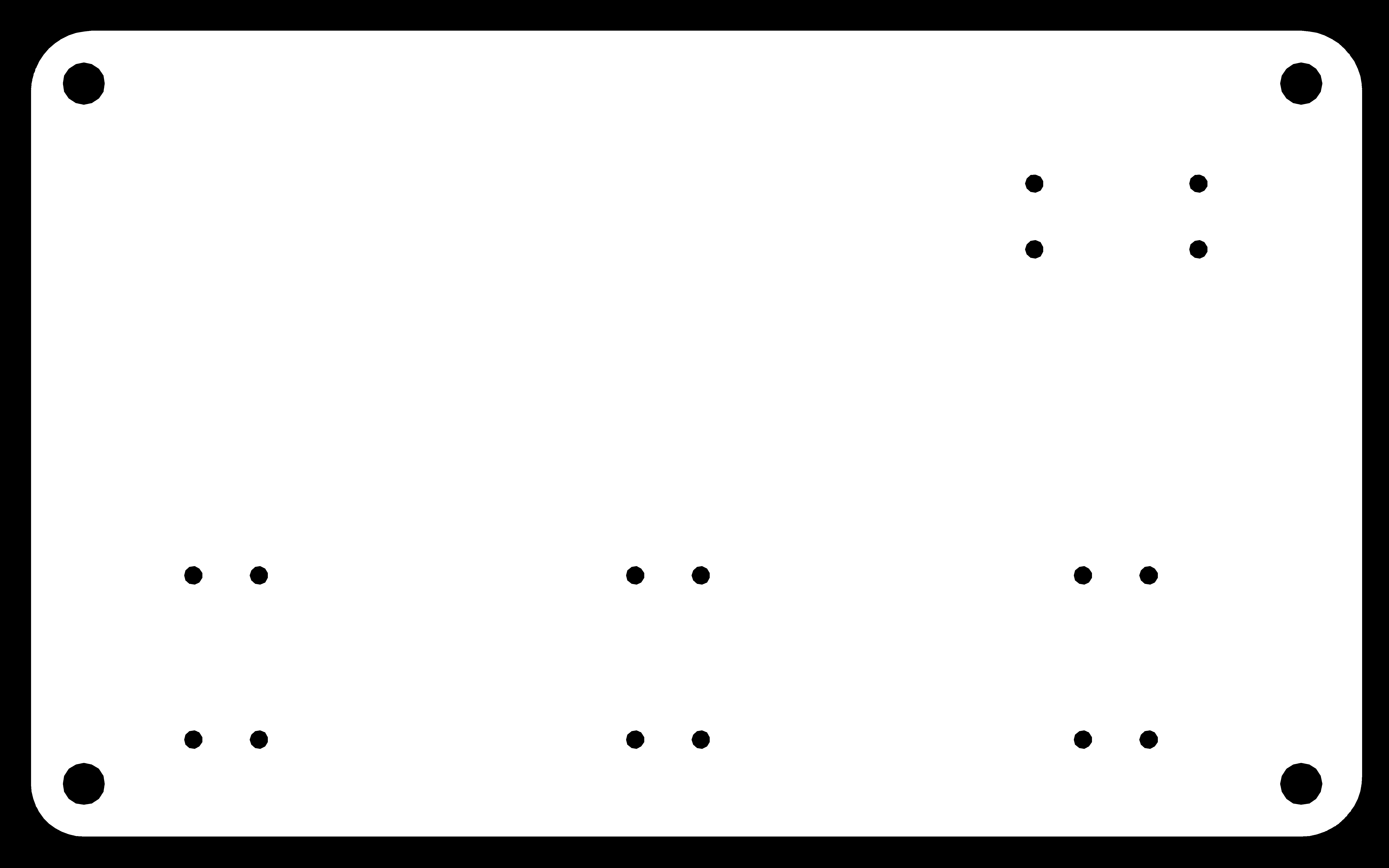
Input board (Switches)
For attaching tact switches, I designed the other input board
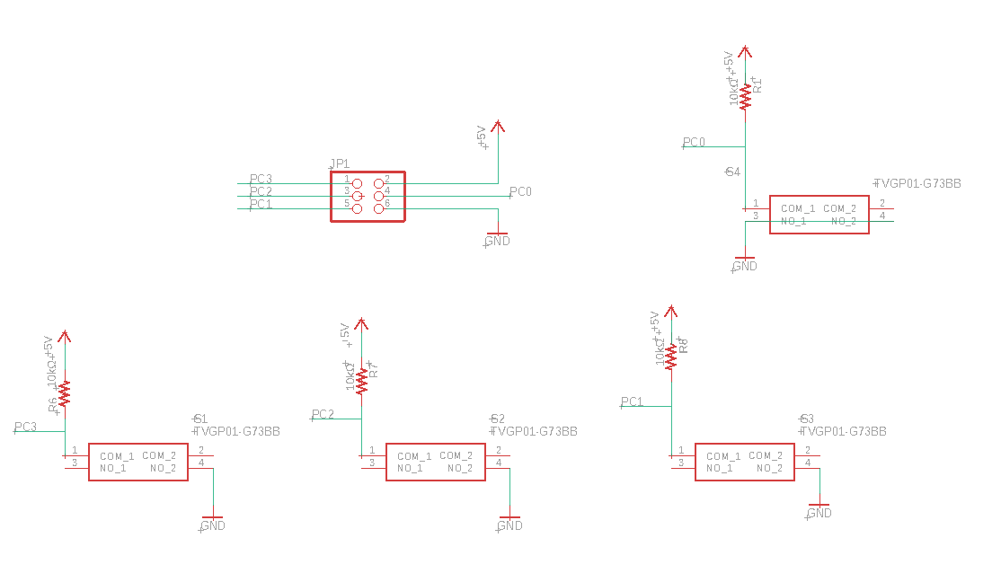
I made this by "1 point earth" that connect Ground line to 1 point for avoiding noise.
However, this is complicate and difficult to understand the connection. Complex path would bring long milling time.Following to instructor Tamiya-san's suggestion, I re-designed input board for switches again.
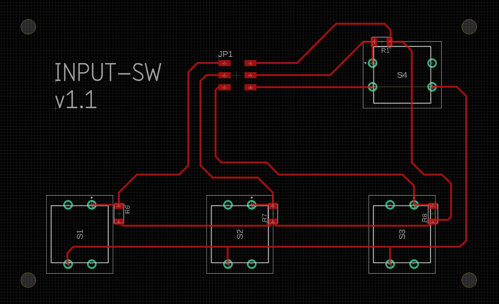
This is much simpler than above one.
Make input boards
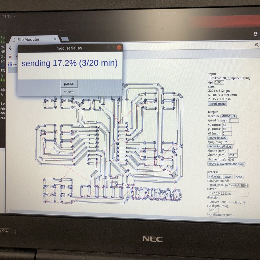
Firstly, I tried mods for milling input board. However, it did not work by some unsolved issue on the xbuntu machine in Fablab Kannai after coming back from staying away days under COVID-19 situation.
Alternatively, I used the other machine that installs Fab Module. Making path and milling the trace went well by 1/64 inches endmill successfully.
However, when I milled outline by 1/32 inches endmill, I failed it because I did not make path and started to "send file". So, I re-milled the board from path of trace.
At the second time, I could mill the board successfully.
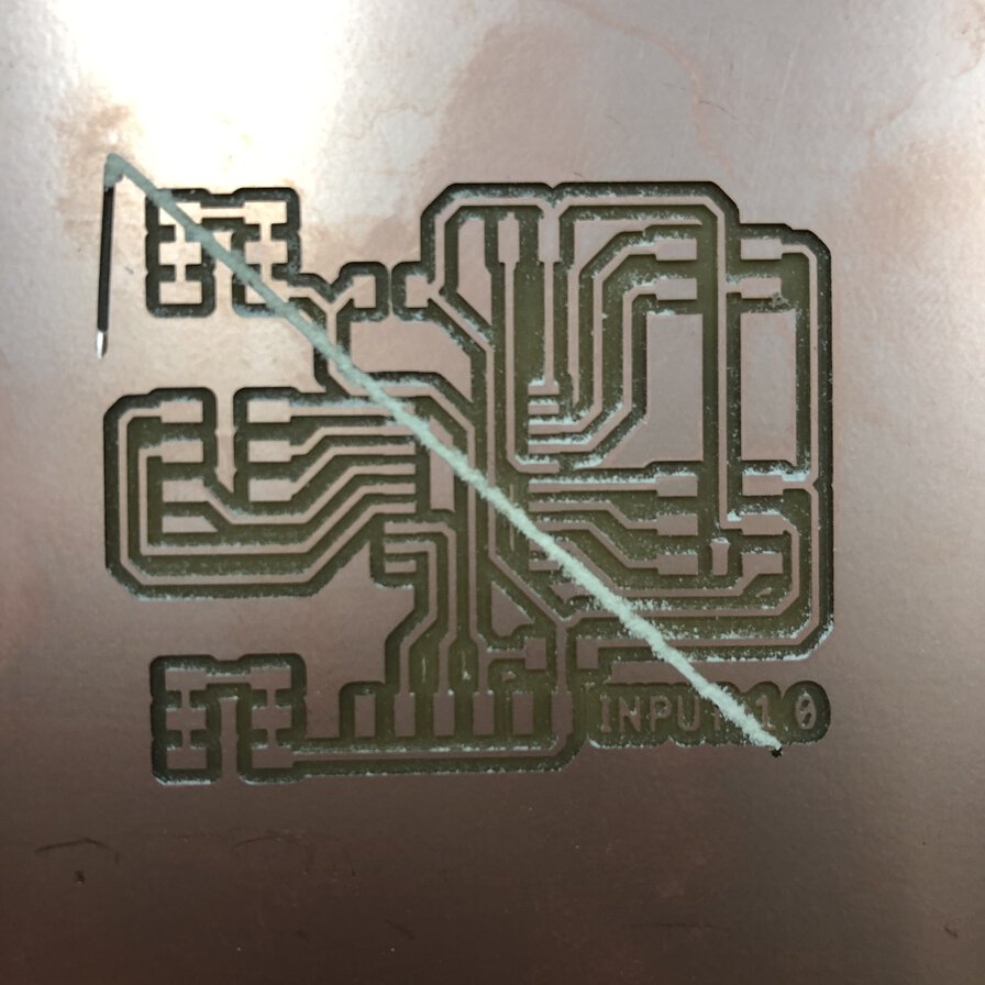
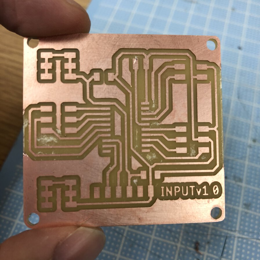
I pealed off unnecessary copper parts by ultrasonic cutter like this picture.
Then soldered the parts:
- ATtiny3216 microcontroller
- Capacitor (1uF)
- 0Ω resister (for bridging over a path line)
- 3x2 pin header x 4 (for 6 potentiometers' Vcc, data pins and GND, for 4 switches' data pins, VCC and GND)
- 2x2 pin header (I2C VCC and GND)
- 2 angle pin header (UPDI)
- 6 angle pin header (Serial communication over FTDI interface)
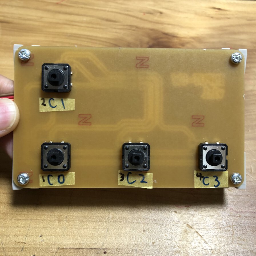
I also created a separated board for attaching tactile switches. This circuit has:
- 3x2 pin header x 1 (for 4 switches' data pins, VCC and GND)
- 4 tactile switches
- Pullup resister x 4 (10KΩ, for each switch)
Making cables for in-out board and switches' board
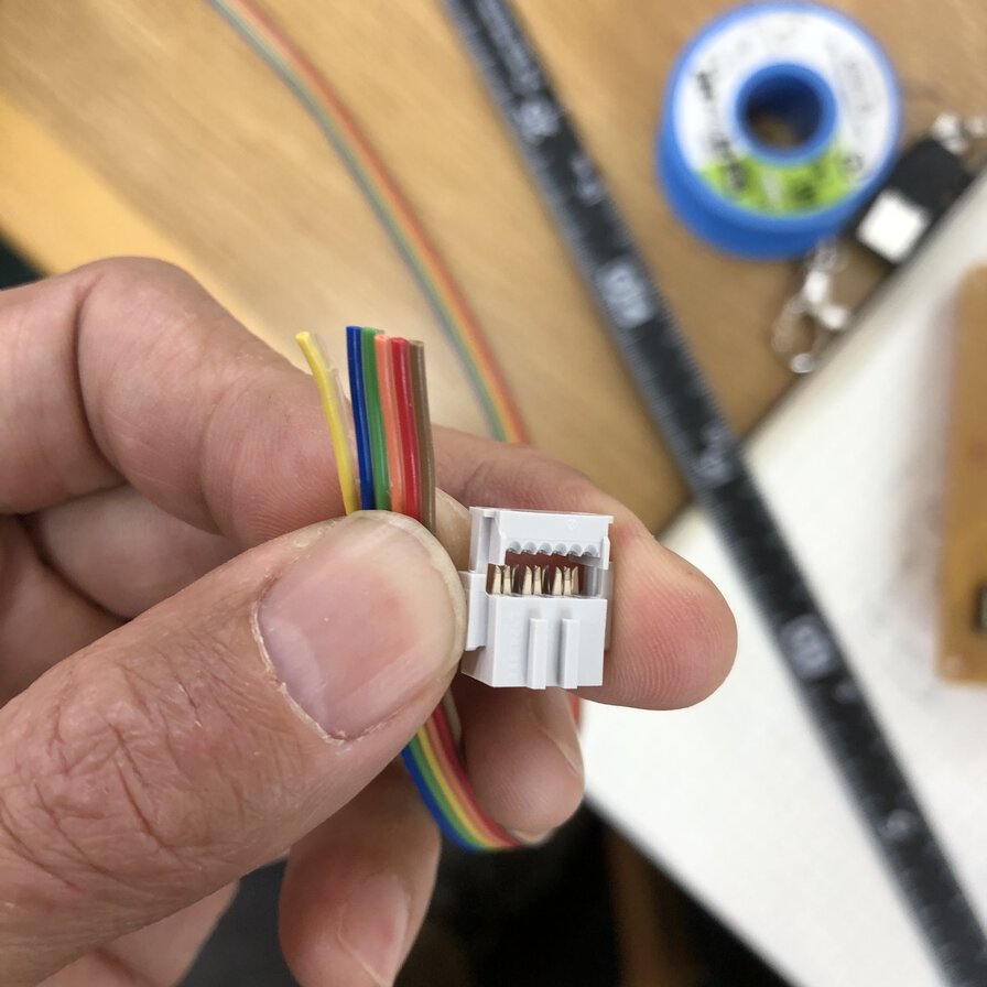
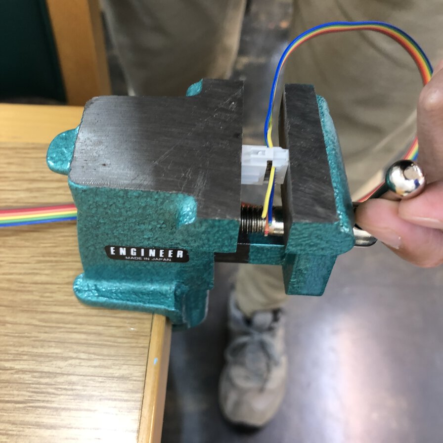
Then I made cables using 3x2 or 2x2 pin sockets using a vice. It's important to make sure the physical pin position is relevant to the other side of cable.
For cable between input board and switch board, yellow cable is for GND. I needed to change the postion of that cable.
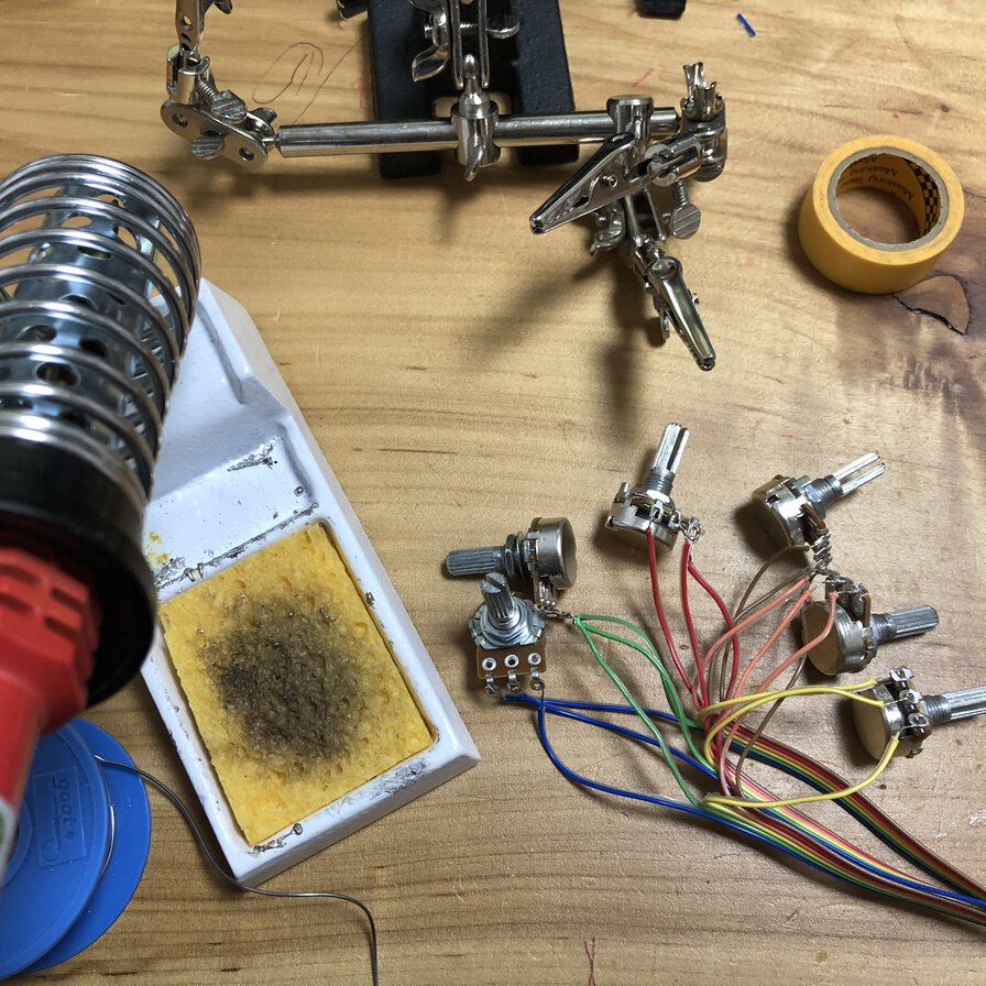
Soldered cables of Vcc, data and GND for each potentiometer.

Connection and test
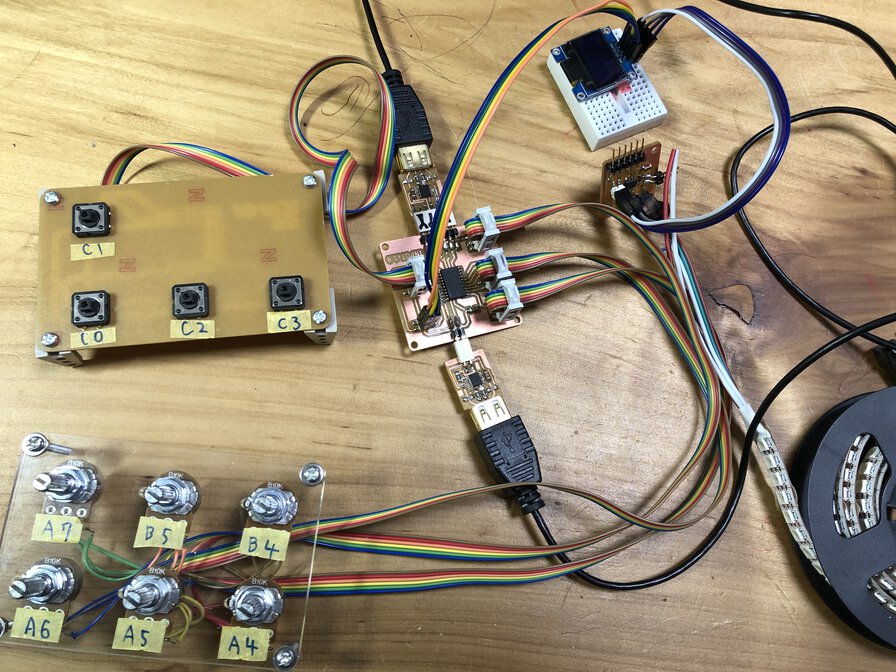
I made simple frames by laser cutter and toy kit parts to attache potentiometer and switches.
Then checked all the input devices(6 potentiometers and 4 switches) worked as I programmed.
Sample code that I embedded to test input board is final_Input_brd_v0.20_i2c.ino