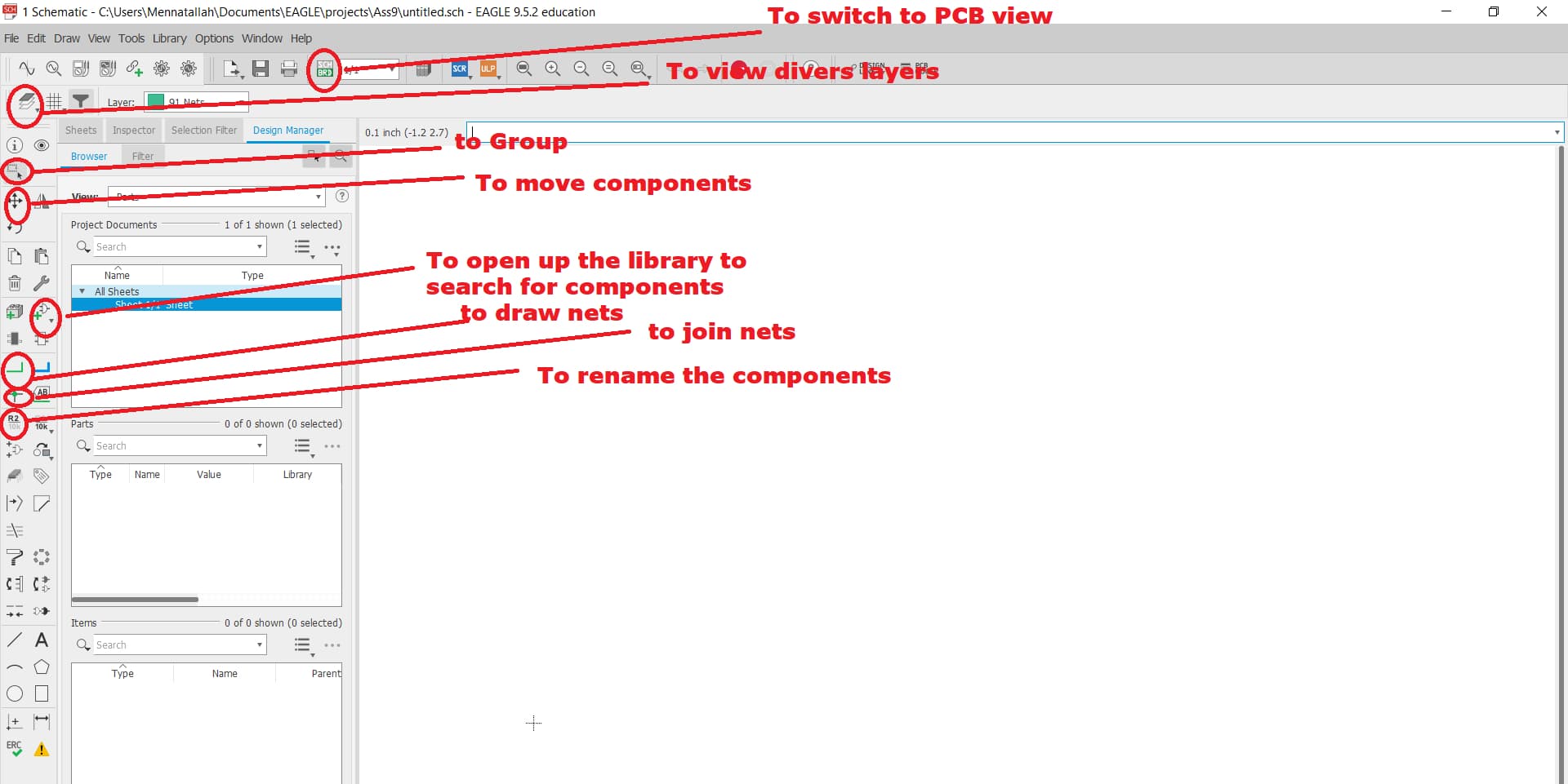
Eagle is an open source software from AutoDesk that enables us to draw a schematic for electronic circuits and turn it into a PCB ,lately a simulation feature was added ,so we can read the signals (voltage or current )of the circuit.Previously I used Proteus beginner level,I was introduced to Eagle during Fab Academy ,it took me some time to get to know the program and note the common features,I followed many online tutorials ,also there were some sessions delivered by Ahmed Ibrahim that were quite helpful.
Here are the main features:
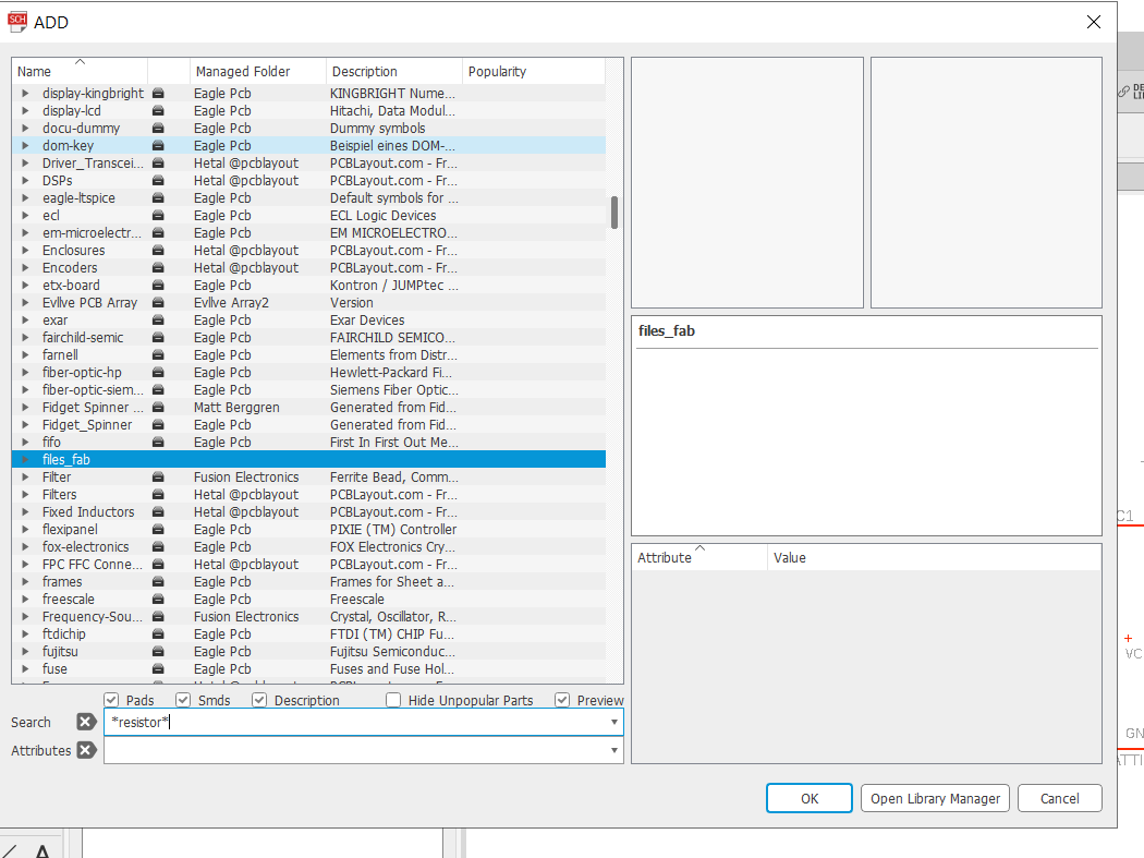
I installed Fab Library:


To begin the design I imported the original files and tried redrawing it as it is:
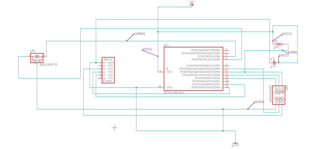
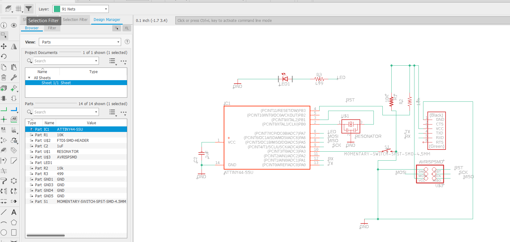
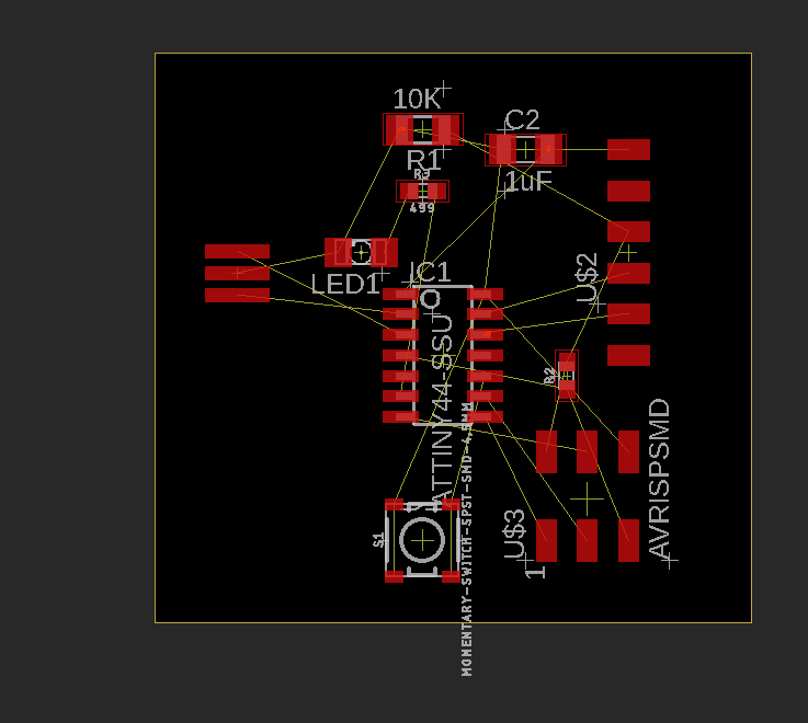
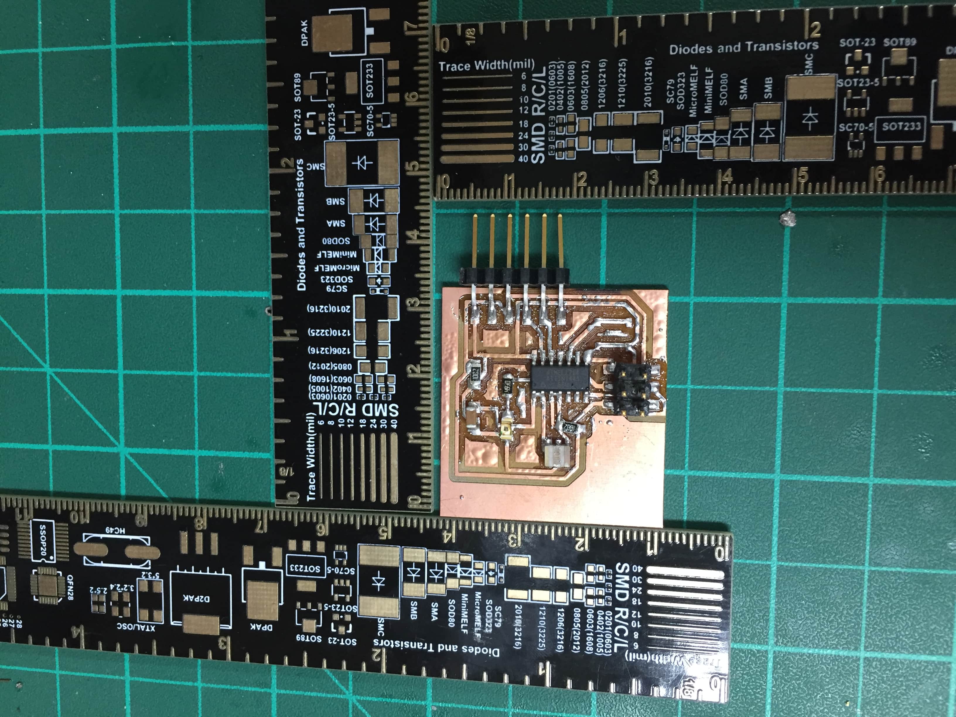
I chose to work on hello.ftdi.44 (Hello Echo board) and add a led and a push button as a start.The components are:
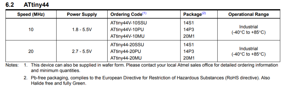
1)ATtiny 44
2)Resistor 10k
3)Capacitor 1 uF
4)2*Resonator 20 MHZ
5)J2 FTDI
6)J1 ISP
7)Push button
8)Led
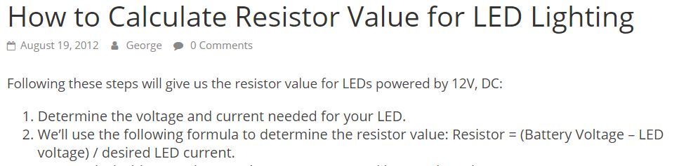
9)Resistor 499 Ohm
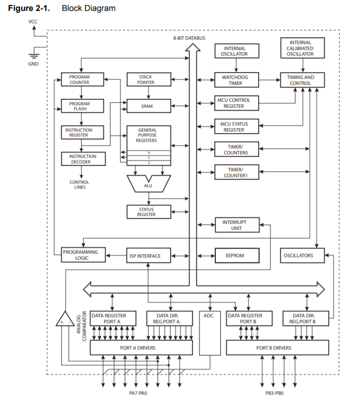
I searched the data sheet of ATtiny 44 about the ports and needed voltage and current to operate the led and push button also to calculte the required pull up resistors.


After listing the components ,I began searching for item by item in the library I can write the components name between *-* so every related component in the search come up.
Then connecting the components:
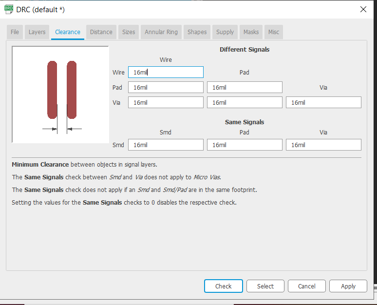
After finishing the schematic ,I switched to board to place the components and rout the wires ,but first I have to set the design rules acording to Fab Lab Egypt's .
Here are the steps I followed to adjust the design rules:

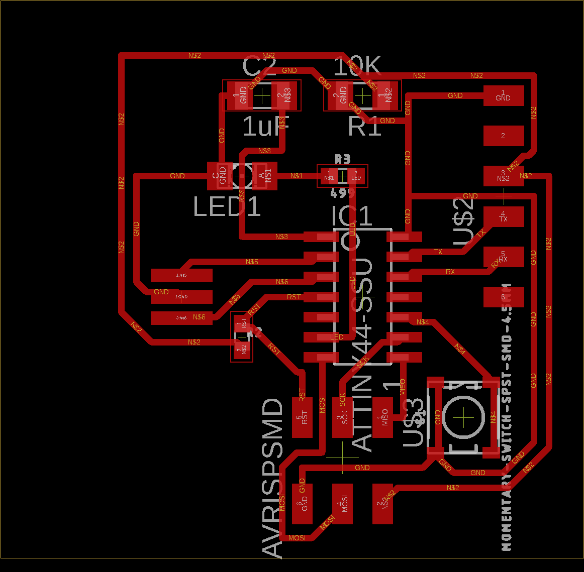
Then I tried different combinations of components placment and did autorouting till I got 100% complete :
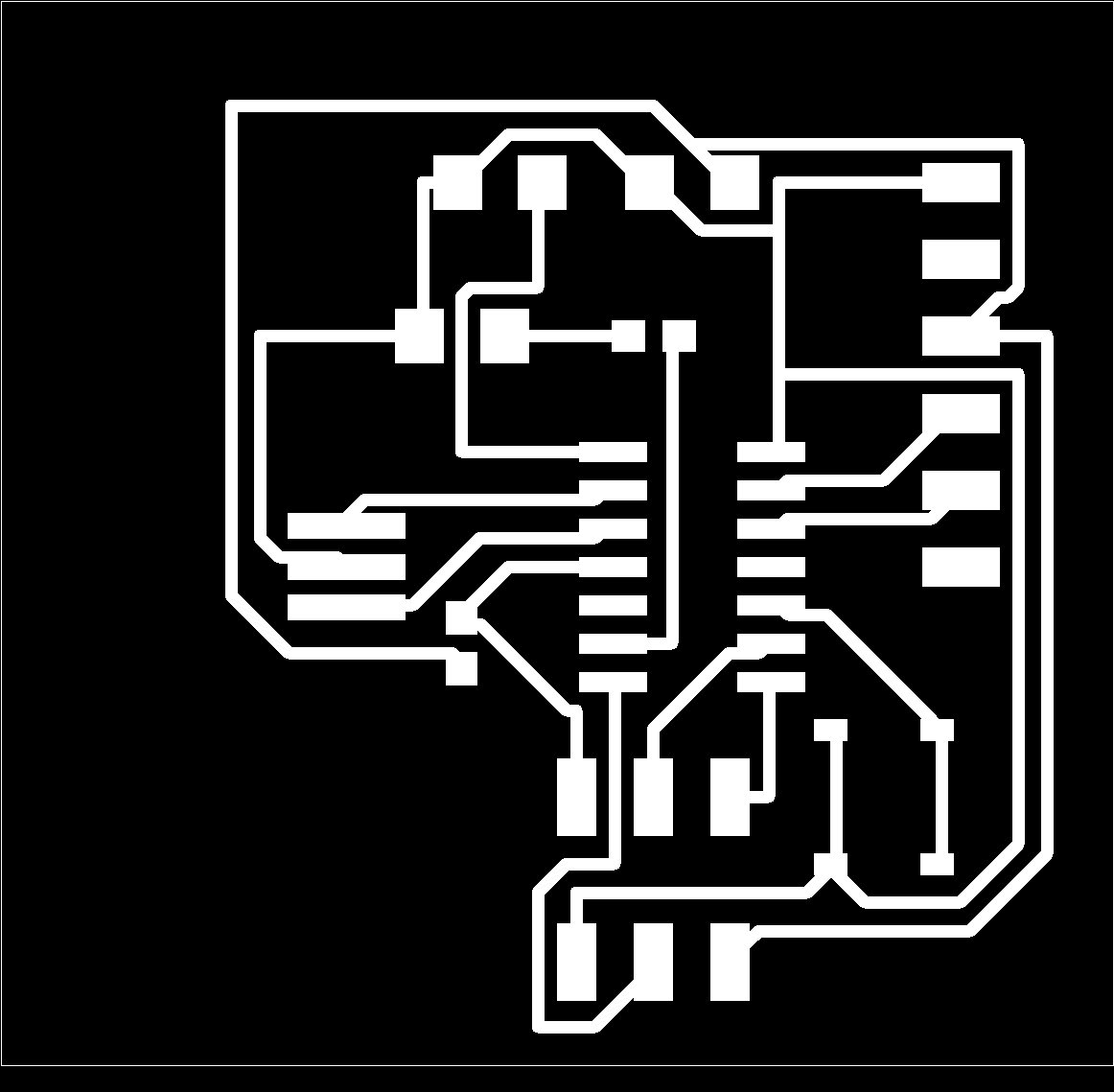
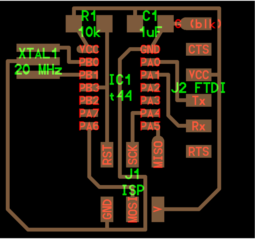
Then I exported the top layer as PNG for the traces:
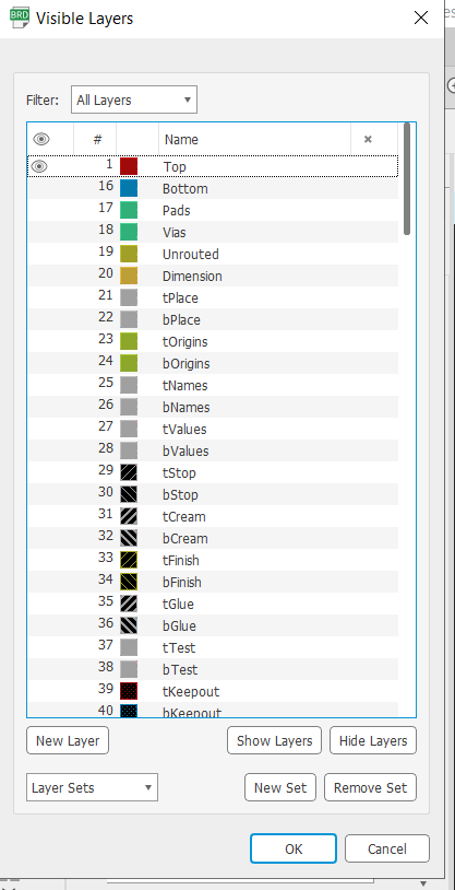
And the dimensions layer also as PNG for the outline:

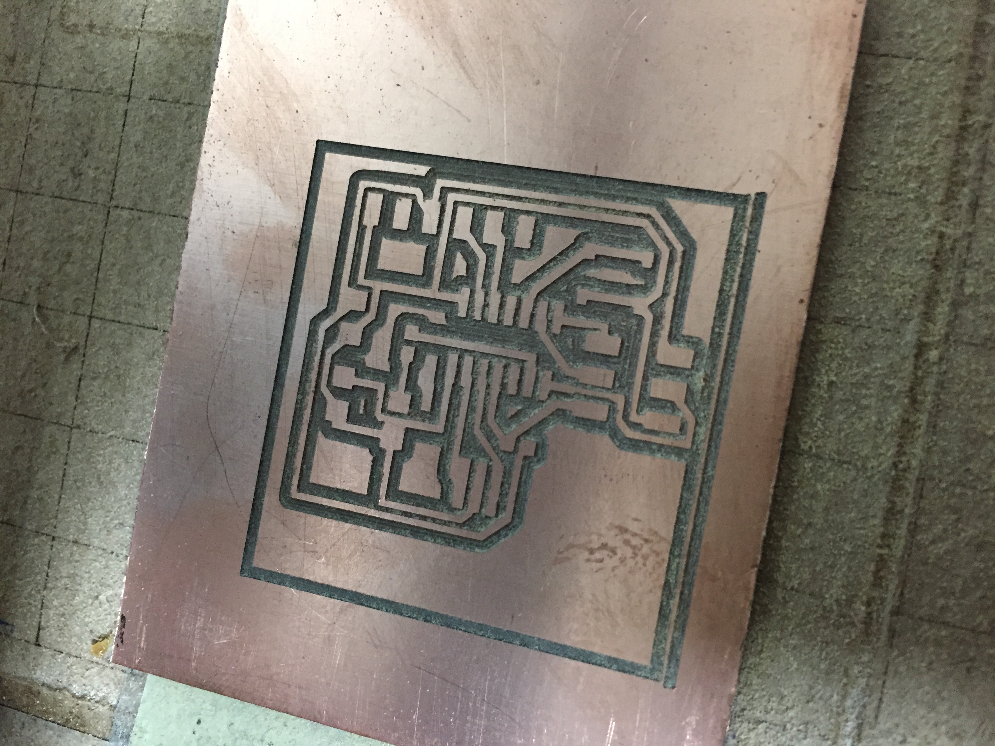
After completed routing, I have to test the board. By testing here I mean printing the layout on a paper and placing the components to make sure that I chose the right package and the adequate foot print.
After week 4 ,in the Electronics Production ,I gained some skills that I will use for this week's assignment ,I followed the same steps: here is the link:
Electronics production assignment
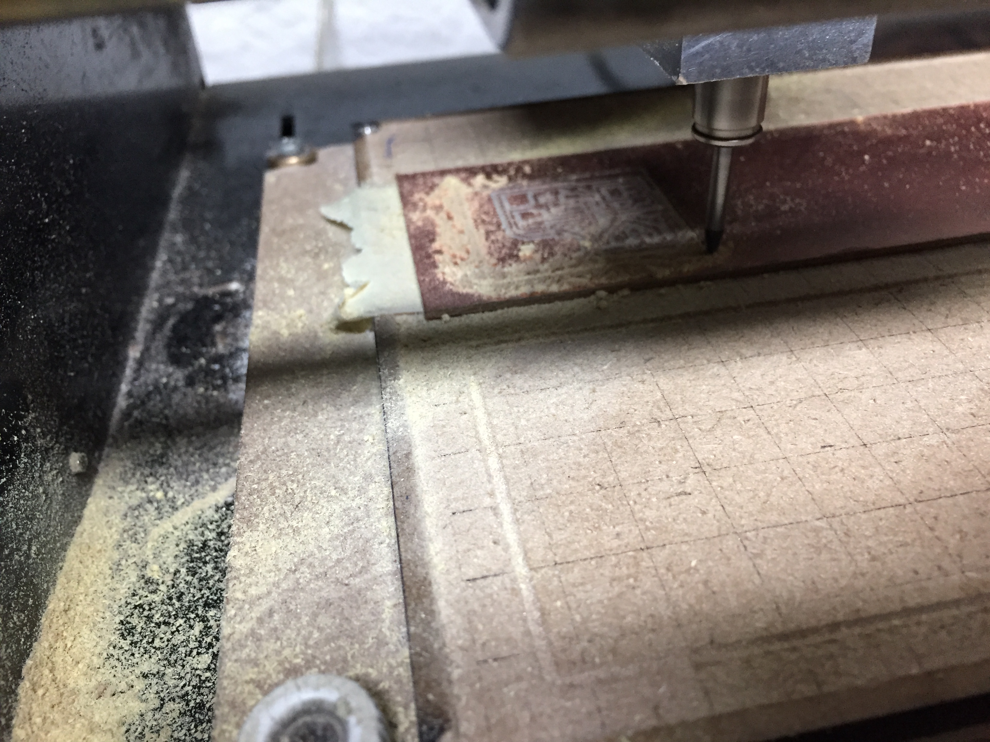

I soldered the components :
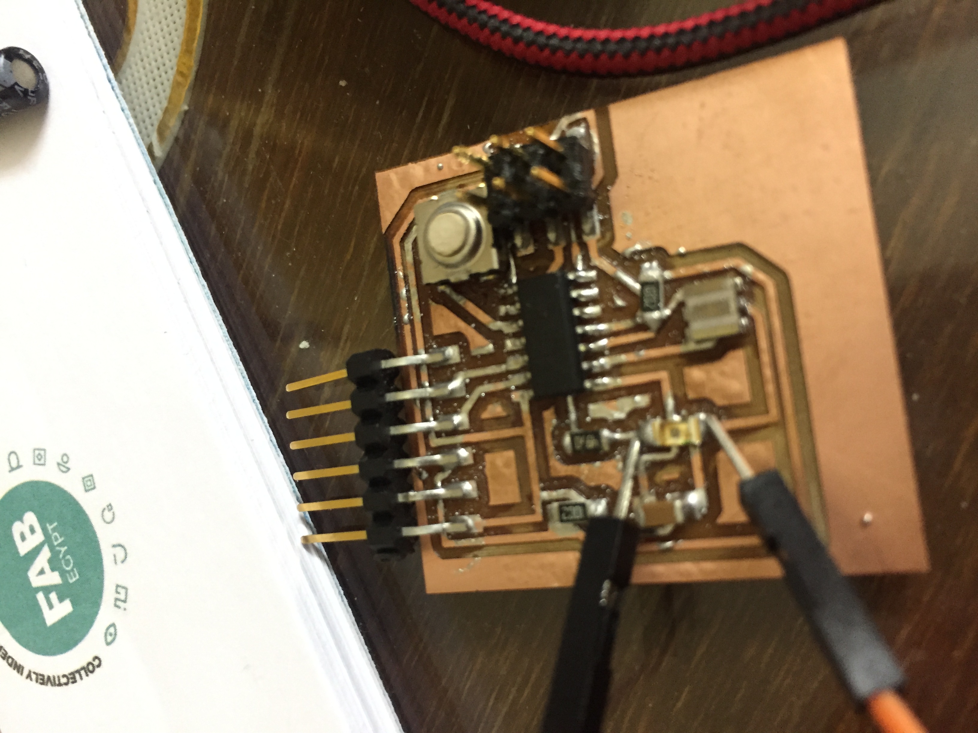
After finishing the PCB milling and soldering ,I have to test it .
First I tested the soldered joints with a multimeter to check if there is no problem with it.
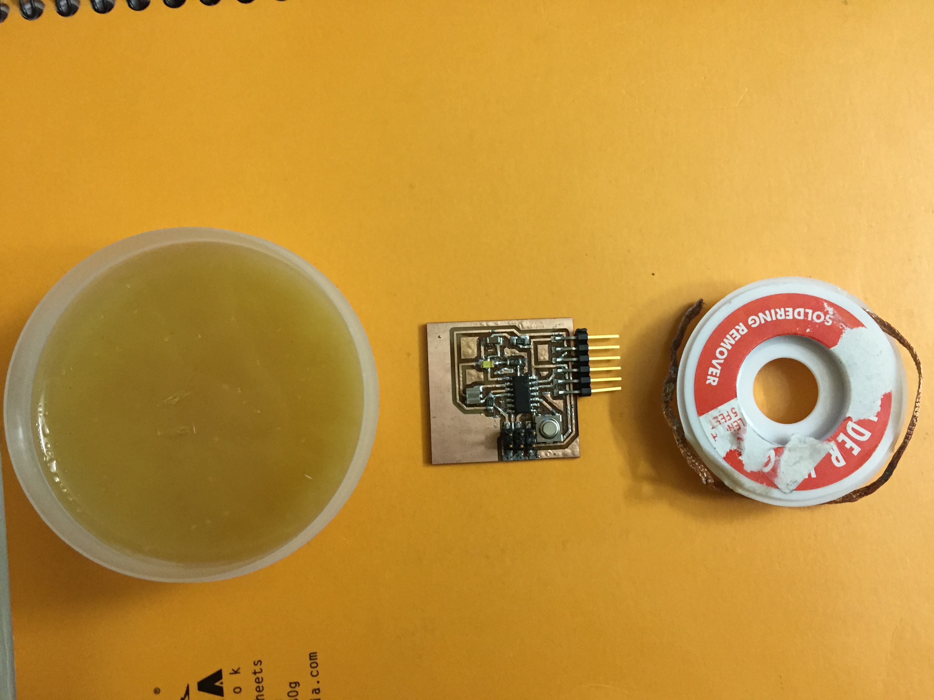
I used Arduino and connected the ground and 3 volt pin to the led and resistor to make sure that I have mounted the led correctly, but the led was burnt,so I replaced it:
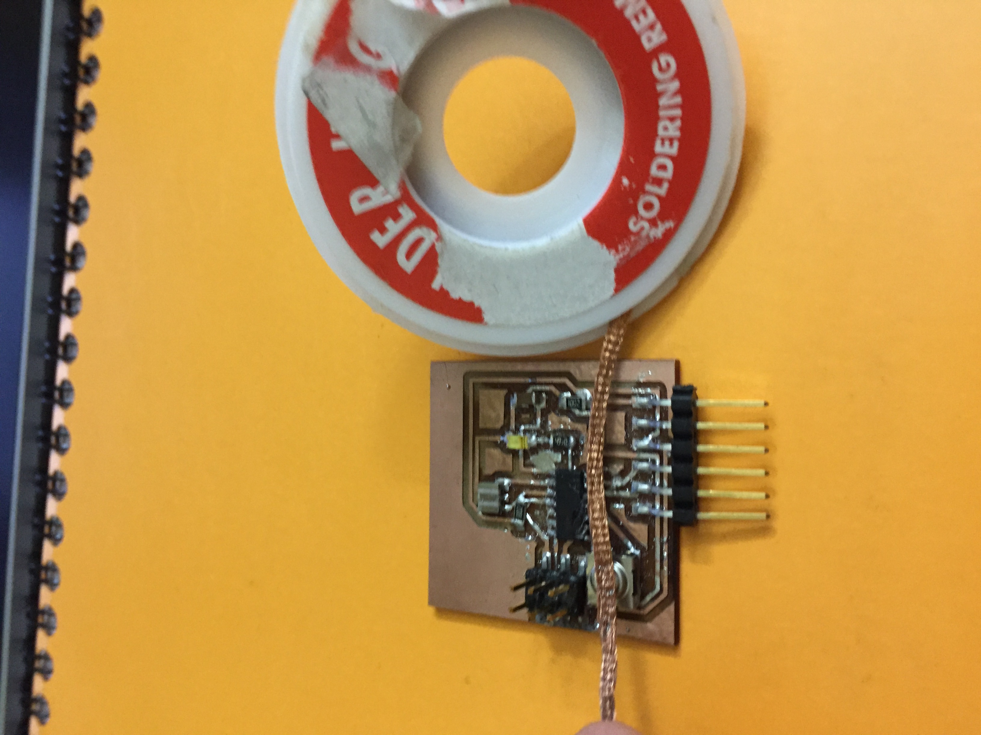
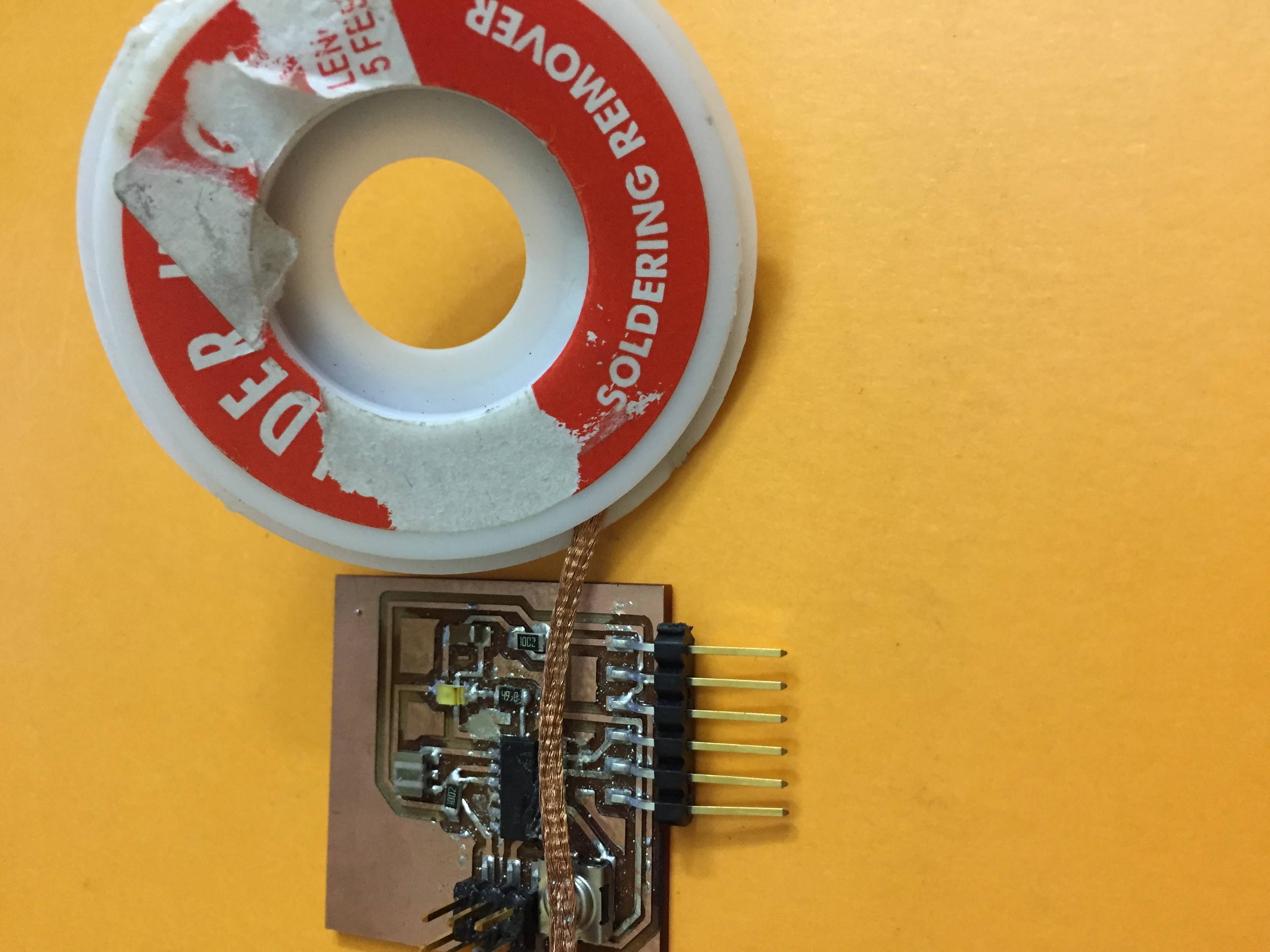
Also by testing for short circuit ,I found many due to excess solder, so I fixed it using flux and wick from the tricks I learned in Week 4 :
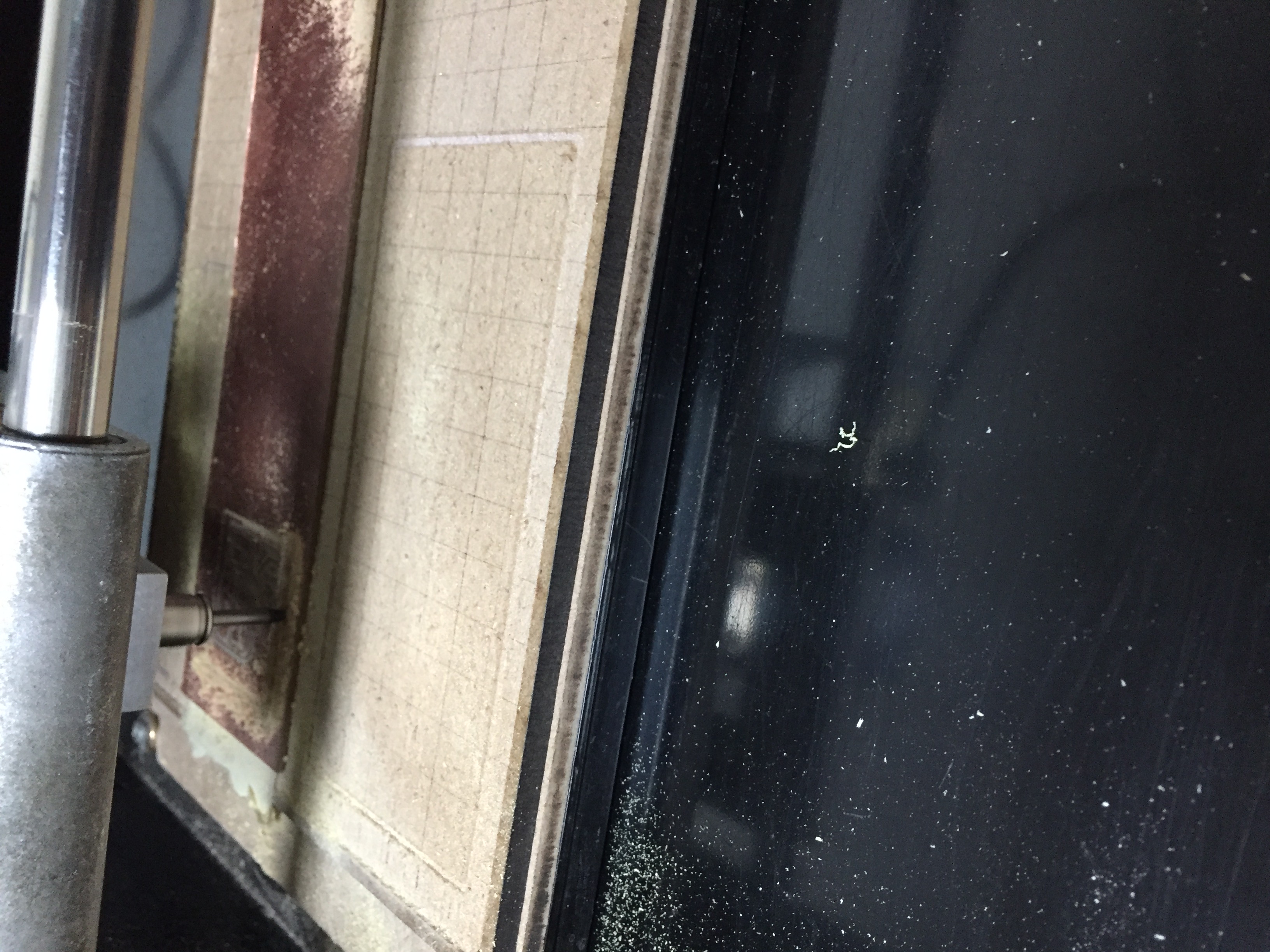
Then to check if the PCB board fuction correctly I connected the board with PC to programe it.
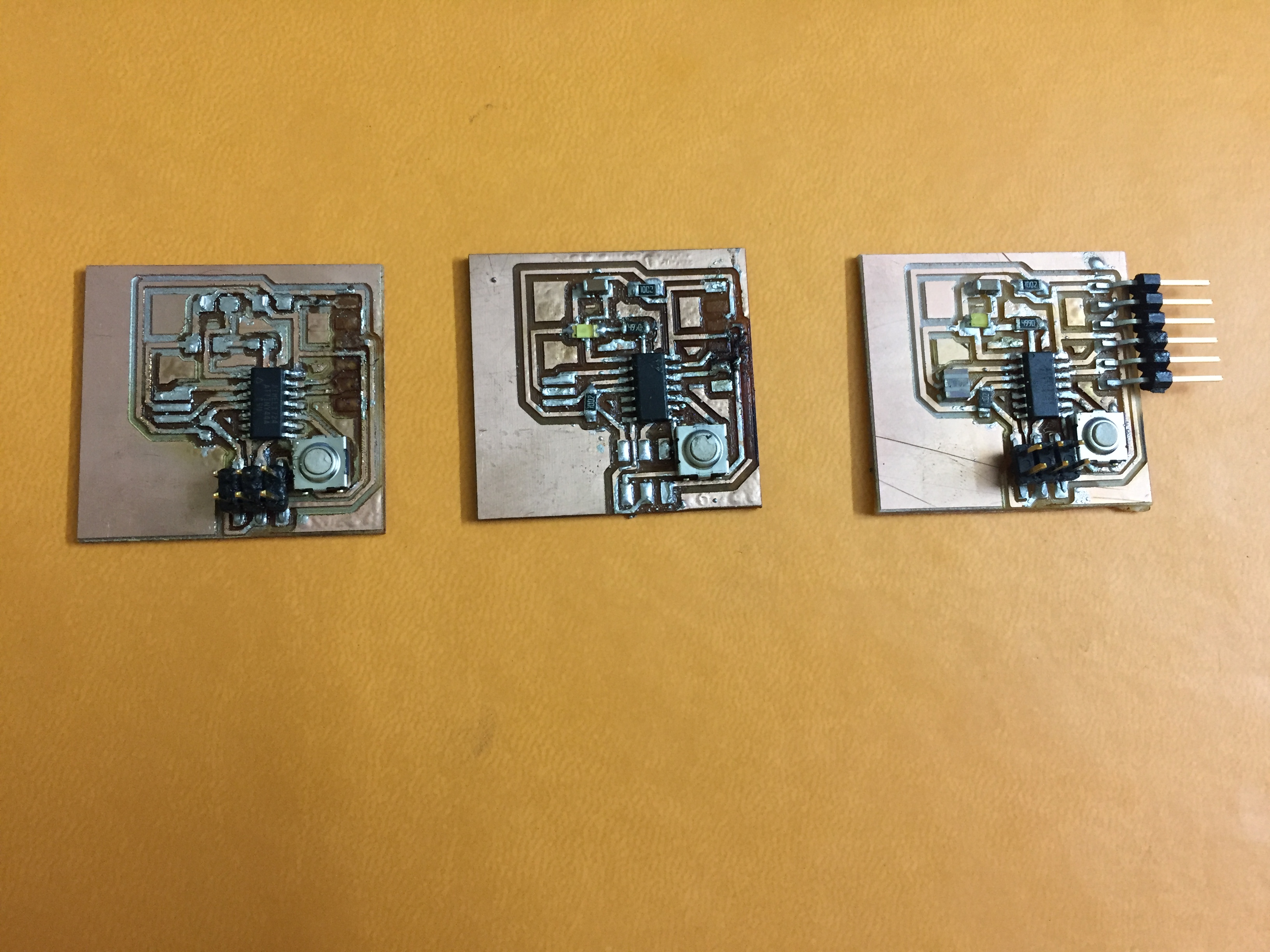
While programming I should have been more careful because while pluging and unpluging the wires ,the FTDI junction broke and the traces were removed, that is why I produced 2 other boards:
Here are the steps,I used Atmel ICE: