Electronics Design
INDIVIDUAL ASSIGNMENT
So my objective for this week
- To redraw the eco PCB without any modifications and test it with
- Make the eco PCB modification to add a led and button.
- Make the last version with an artistic touch.
So in the beginning, I was going to use easy software like fritzing but I was starting to like fusion 360 and when I know from the lecture that you can use eagle and fusion together I thought it will be good for the final project so I can integrate the PCB with the cad design, I started with watching SparkFun eagle tutorial as the instructor recommended and it was really helpful.
Now it’s time for action so the first thing I did after installing eagle is to add fab academy component library it did make my life easier.
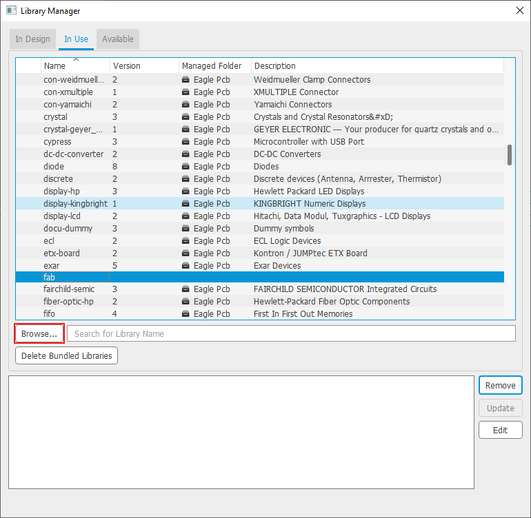
To add fab academy components library open “Library Manager” and from “In Use” click Browse and select the fab library, now you can use the fab library.
So if you’re new with eagle I will start to explain it in an easy way.
You can say it’s the main to layers is the schematic and board
Frist with the schematic it’s a representation of the elements of your circuit diagram, Second the board it’s your final shape for the circuit.
Note this Definition is from my own perspective and if you want to know more I advise you to watch the tutorial, anyway its time to choose the eco bord that I will replicate.
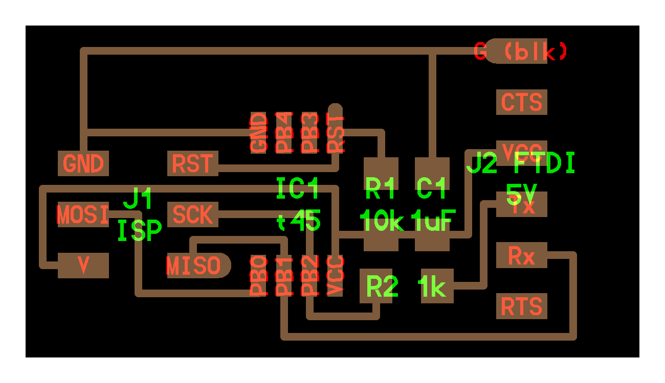
First I will start with Redrawing “echo hello-world board,”, I will use Hello Board "ATtiny45" from Neil as a reference, After creating a new Schematic it’s time to add the hello-world board components
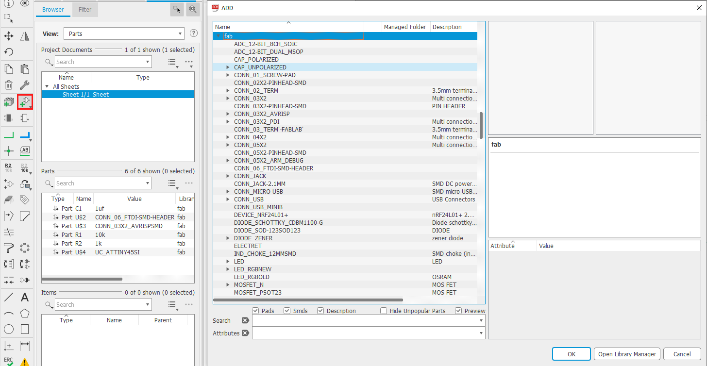
So the first step is to add the electronic components from “Add Part”
Next is to connect everything together at first, I used the “Net” tool to connect everything but it looked messy and I couldn't keep track with every line, so I used a tool called “Lable” with “Net” to keep everything Organizer
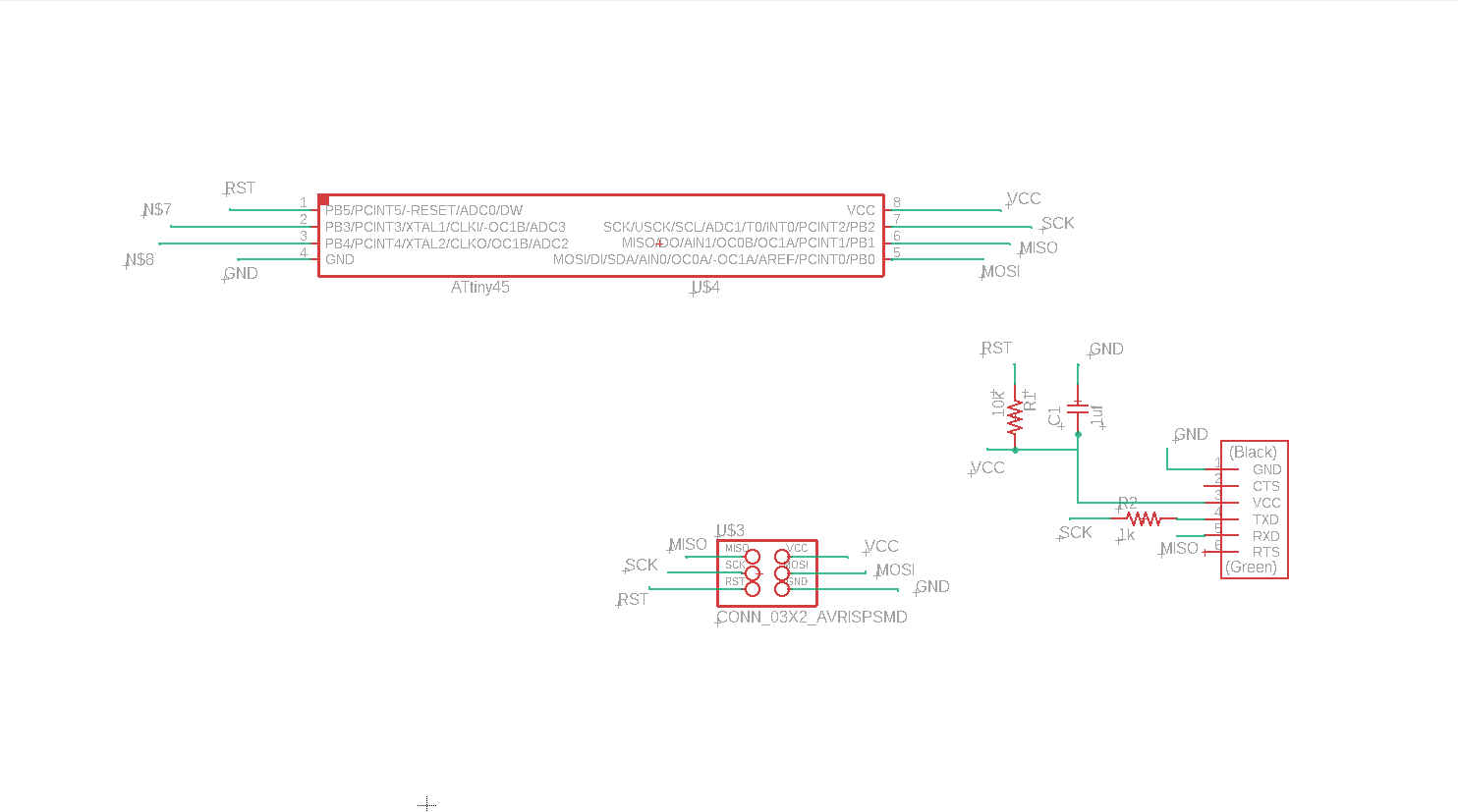
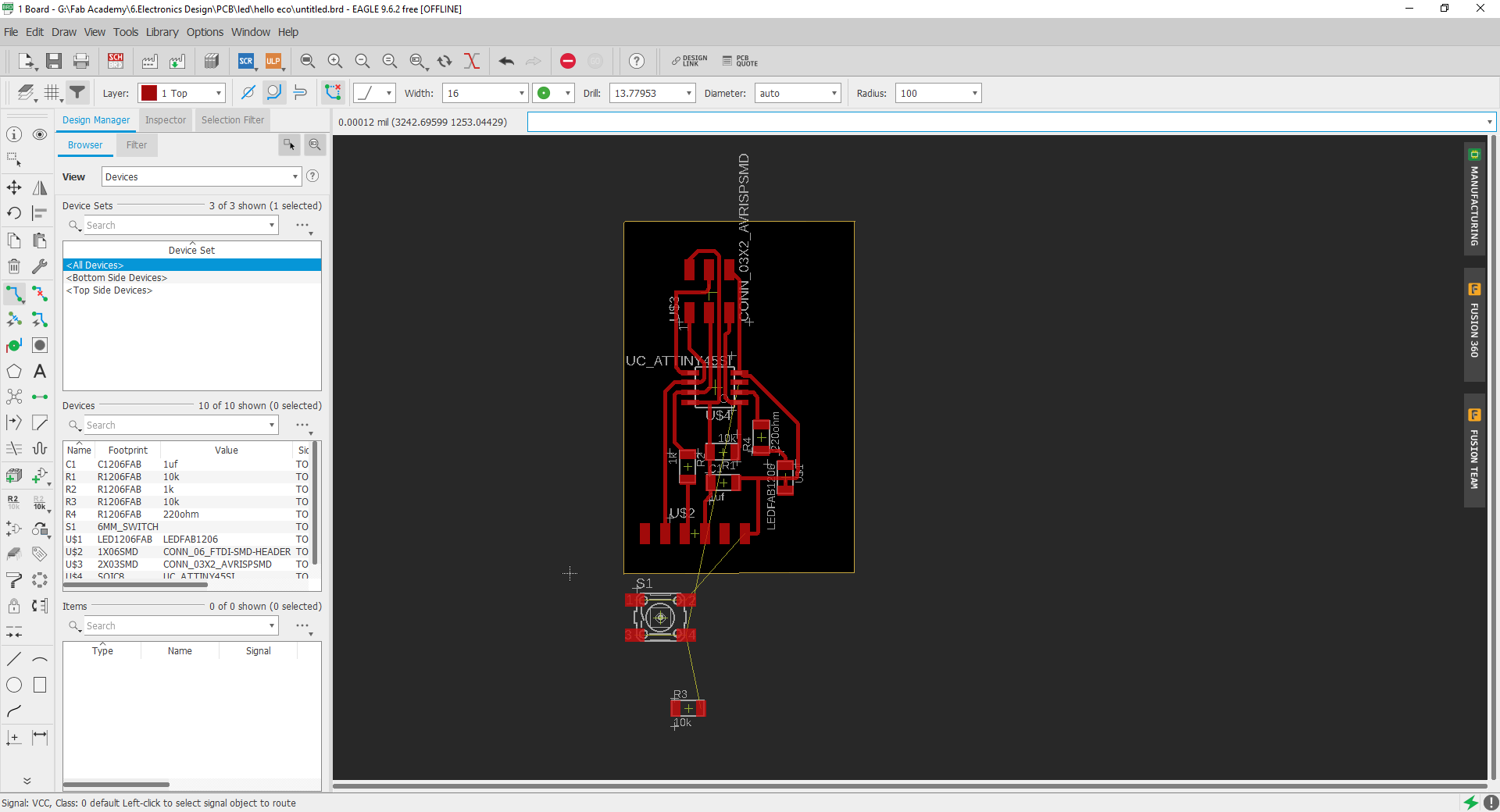
Last is to make the PCB board layout, to make everything easier I learned a small track is to start with the component that has a lot of pins and put it at the middle of your PCB, And arrange and connect everything.
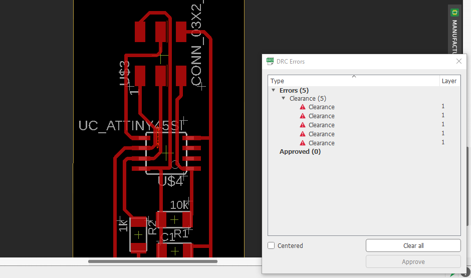
The last step is to make “DRC” check to be sure that there is no miss connection or overlap, To do that first to select "DRC" from "Tools" next is to select "Clearance" so because I know that the endmill clearance is 16mill so at least I have to make the clearance between trace and other 16mill.
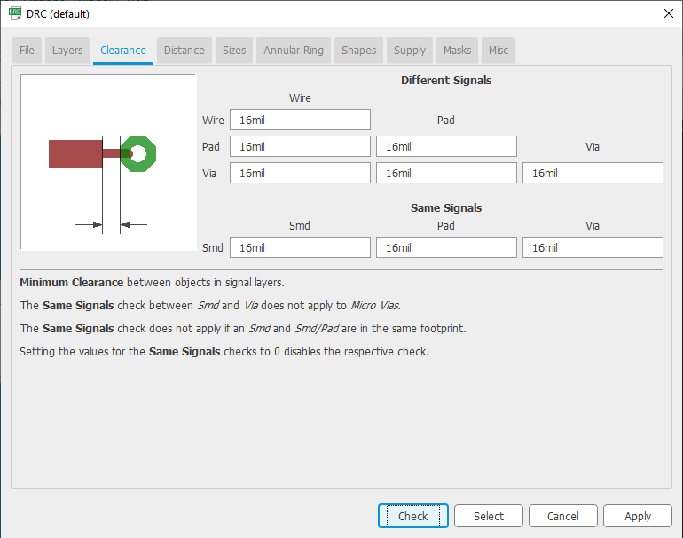
After checking there were some Clearance errors it was easy to fix just move the traces until the error disappears.
Now it’s time to export and mail the PCB as explained in the Electronics Production
Week, so after a long morning with cutting and soldering everything to gather, it’s time to program the “Hello Board” with the ISP
cd ./the file direction "
Next
sudo make -f hello.ftdi.45.port.make program-usbtiny
And if everything goes well you should get this message.
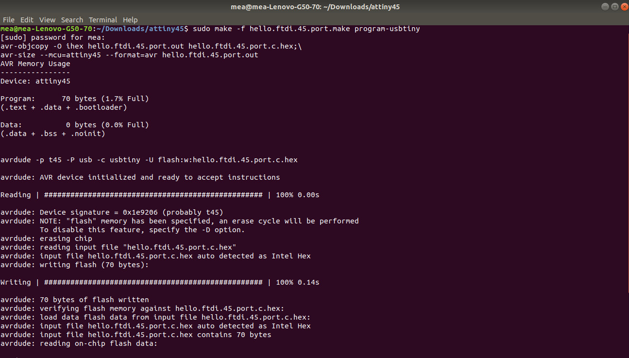
Ok it wasn’t that hard to program just type a simple command and it’s done
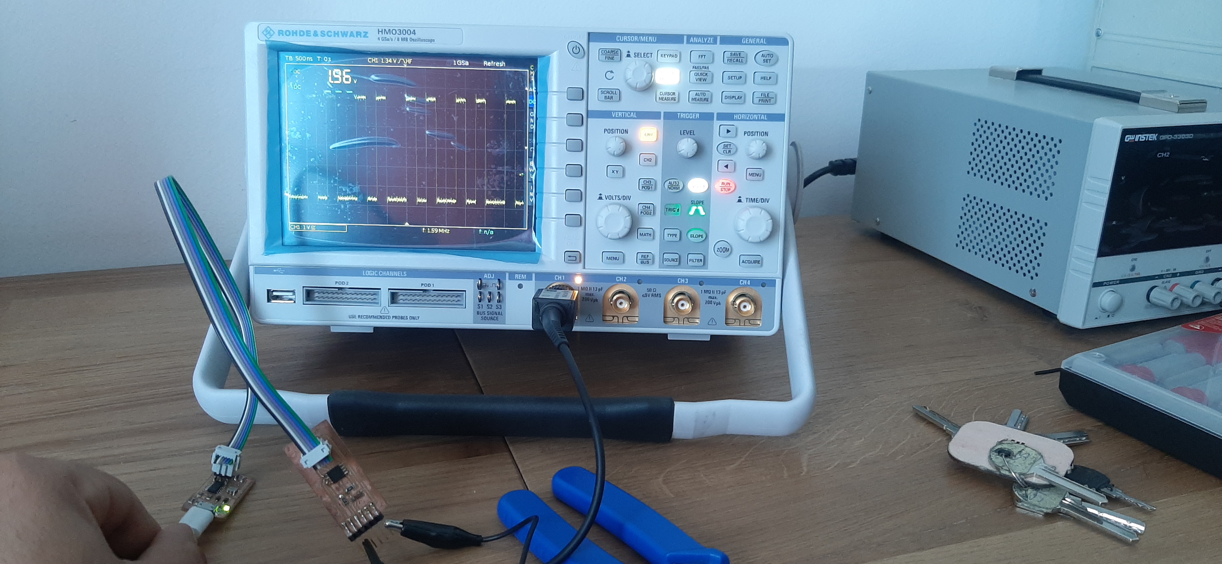
oscilloscope
And lat’s test the PCB on the oscilloscope, So I have at my work a new oscilloscope but I have considerate that I didn’t use the oscilloscope before and like everything new you try to use you are always afraid to make a deadly mistake and break it X”D
So before I try to use it I began to search about how to use it and found this great video that explains How NOT To Blow Up Your Oscilloscope!
So as I understand if I used the oscilloscope with a close circuit there is no danger, it would be a problem if my circuit was shorted somehow with earth, now testing Time.
So the code I have uploaded to the PCB it should make square waves from 0 to 5V so I will use the oscilloscope to see the square waves
Hello echo
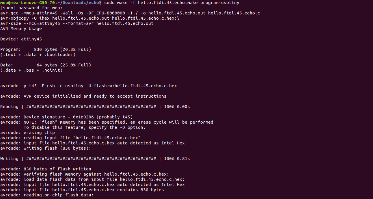
Now to test professor Neil echo.c code, so as I understand I can reprogram or flash code on Attiny for 10.000 times.
As before I will need to download professor Neil c codes {1,2}, So I need to do the same as before first to go to the code direction and type.
sudo make -f hello.ftdi.45.echo.make program-usbtiny"
And again if everything is ok you should see a massage like this.
Add a led and button
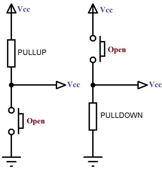
So I make a copy of “echo hello world board“ and I did a small modification is to add a push button and led, so now I need to figure out which technique I will use to add the pushbutton pull-up or pull-down resistor so first I need to know the definite between them.
A pull-up resistor is a resistor connected between a signal and a positive power source, pull-down resistor is a resistor connected between a signal and a ground.
The Differences Between Pull up resistor & pull down
|
Pull-Up Resistors |
Pull-Down Resistors |
|
Connect between I/O pin and +supply voltage, with an open switch connected between I/O and ground. Keeps the input “High” |
Connect between an I/O pin and ground, with an open switch connected between I/O and +Supply. Keeps the input “Low” |
|
More commonly used |
Less commonly used |
So I will use Pull-Up Resistors, now after I coped “echo hello world board“ now it’s time to make small changes.
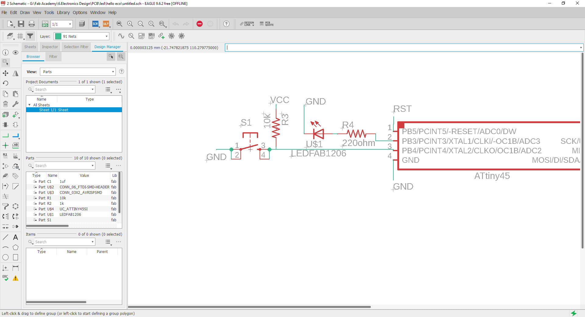
After I added the Pull-Up Resistors to pin PB4 next is to modify the layout board

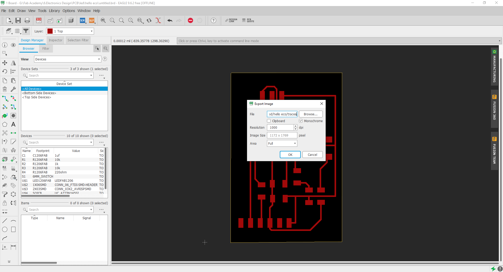
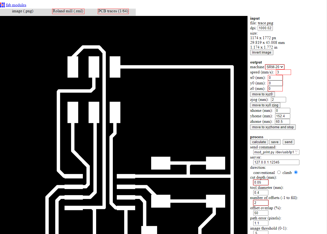
And we are done it’s that simple, next is to transform the layout to real PCB, to do that first I need two images first for the traces and dimension “trace mailing”
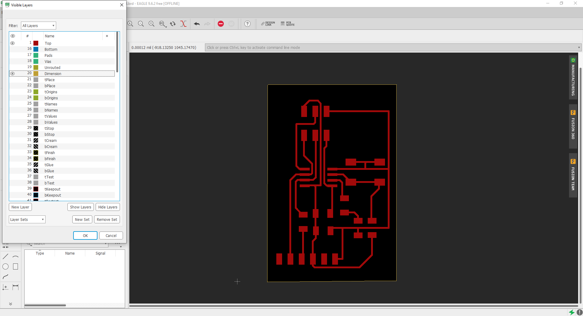
Then export it as an image with the monochrome option selected and with high dpi for me I will make it “1000”
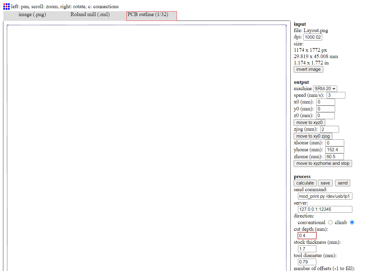
The second image is for the dimension “cut layout” and repeat the last step.
The last step is to use fab modules to convert the image to Gcode, you can use fab modules online from this website
Now we select the traces image and 1/64 endmill
Next after selecting the machine that I will use "SRM-20" Frist, I will change the feed rate speed too 3
And the cut depth to 0.5 and make sure that the machine is leveled next is the number of offsets to two instead of 4 it will reduce a lot of time
And last set the {x,y,z} to 0 and we good to calculate
Layout cutting has the same principles except when you select the different endmill “1/32” and after that the cut depth I will make it 0.4 and I will make the feed rate speed as before
So because I’m using windows to execute the Gcode I will use “Vpanel for SRM“ it’s simple to use
First is to set the new {x,y,z} parameters
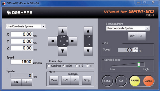
Next is to select “CUT” and from cut choose your G code and click output now I have my PCB done, the final result
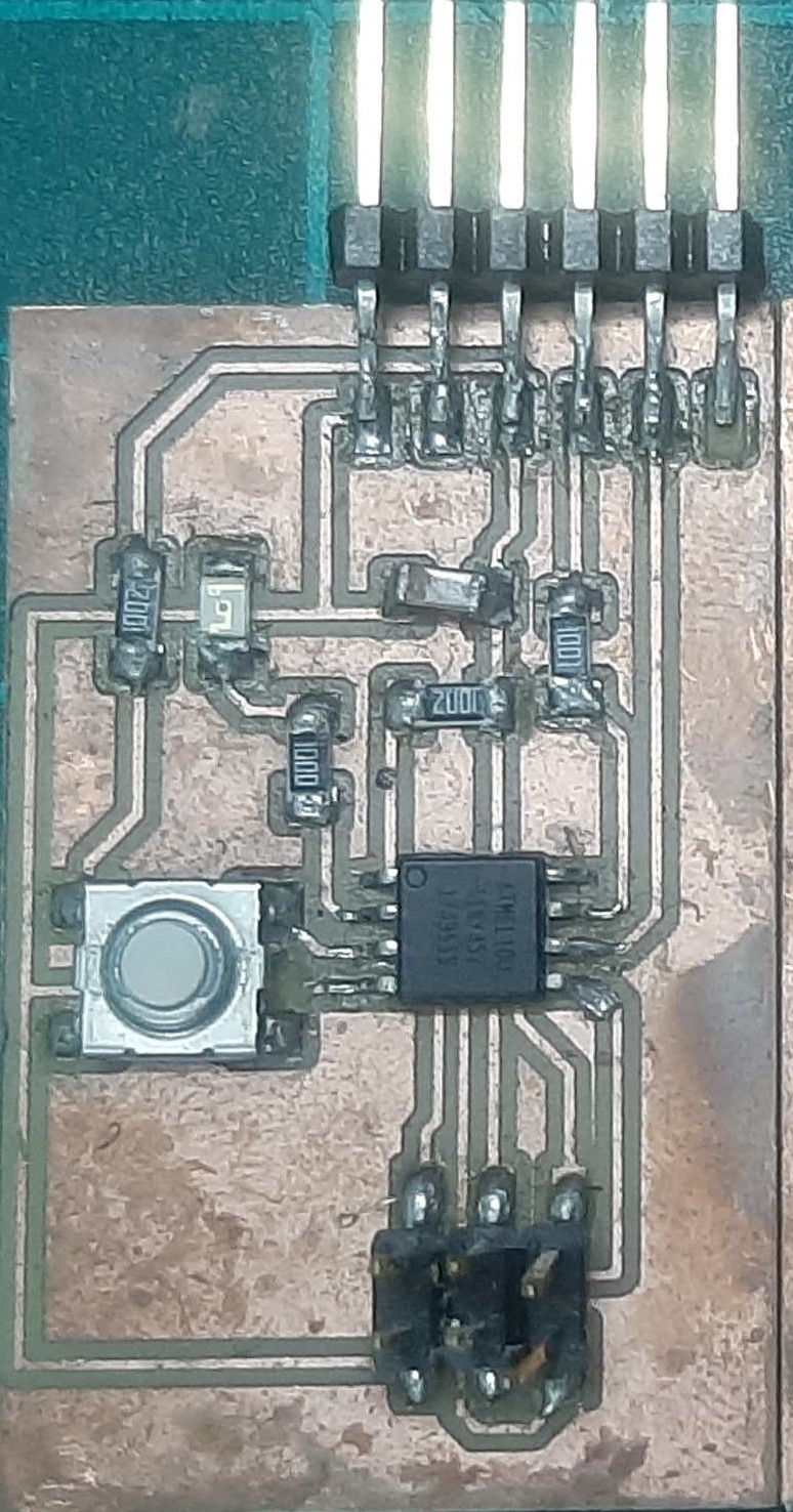
SO I will programed the PCB you will find it in “Embedded programming week”
But that wasn't changing enough so I decided to make the final PCB with an artistic touch.
the last version.
So when I was brane storming with my self for a cool idea I damaged making a PCB like a butterfly and the main controller in the middle and Leeds every ware at the wings and controlling the lights with how many time I will bush pushbutton, I think it will be a great board for the embedded programming assignment.
So I started with google for a butterfly pic that could fit with my plan.

Now I need to think how I’m going to import this pic, the first idea came to my mind to outline the pic using illustrator cand convert to DXF so I can import it to the eagle board.
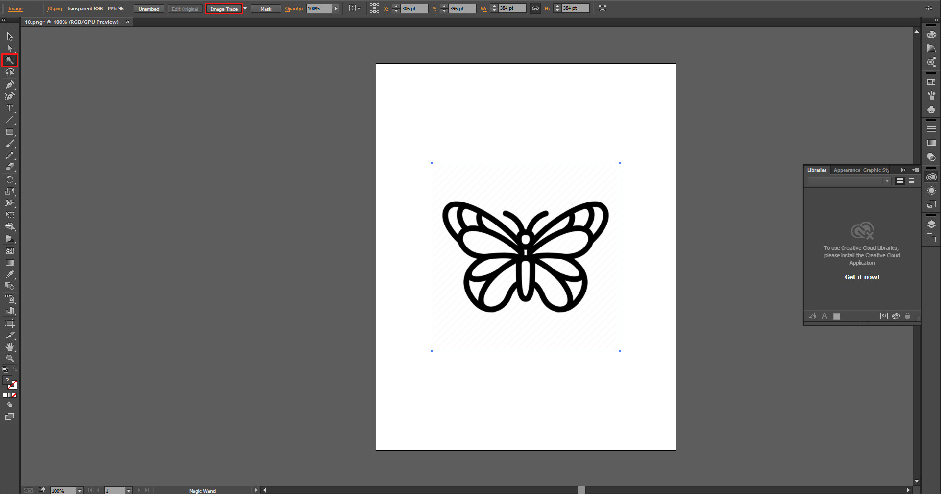
After I opened illustrator I used “Magic wand tool” to make “Image Trace “, Now I will use the “Expand” tool to convert tracing object into paths, last is to use the “Magic wand” again to select the black color and convert it to wight so we can see the outlines.
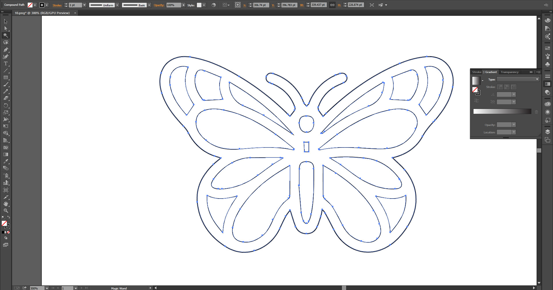
Well, now we can export to DXF.
Failures.
So every time I try to import the DXF what happens is either nothing or import small parts from the total shape, I did what anyone will do that to google the problem and I found a lot of solutions but none of them work one of this Solutions is to use eagle “ULP” and I trayed most of the ULP I could found theو same result I think the shape was complex enough.
By luck when I was an experiment with fashion new tools I found a tool called “Creating a 3d PCB” and when I selected it asked me to select the PCB or in another meaning the out shape of the PCB I want to put the components on it, and by default, I trayed to import the DXF from illustrator to see what will happen.
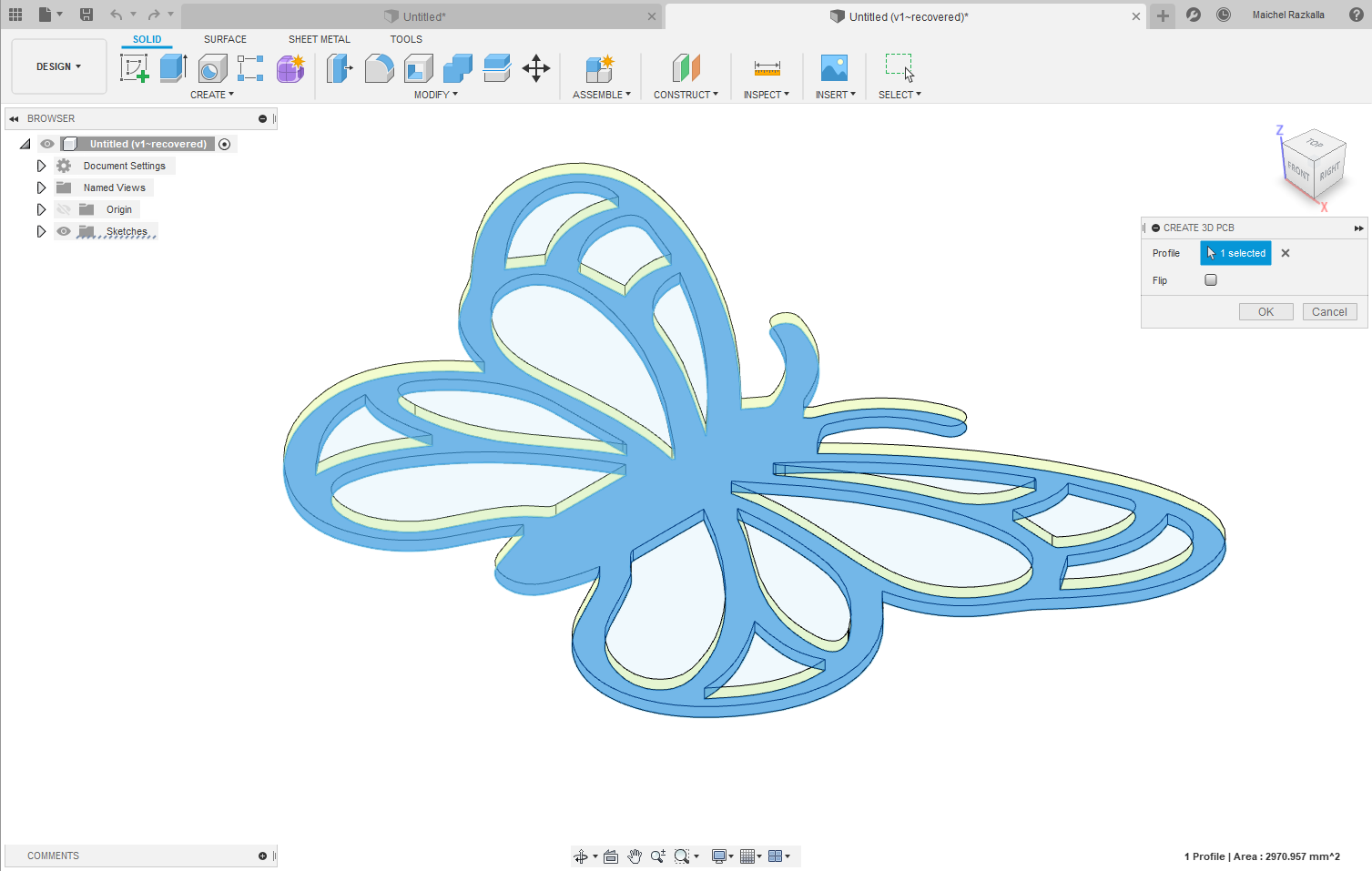
Next, I selected “؛Push to 2D PCB” I was expected that it will reflect to eagle but what I have found that I can draw a full PCB with fusion and I found that fusion has his own components library, and I found that I can export the PCB as “.brd” so I can import to eagle later but after a lot thinking that I’m going to drow this PCB on fashion, it will be amazing if I can make the PCB and cad and cam from only on the program .
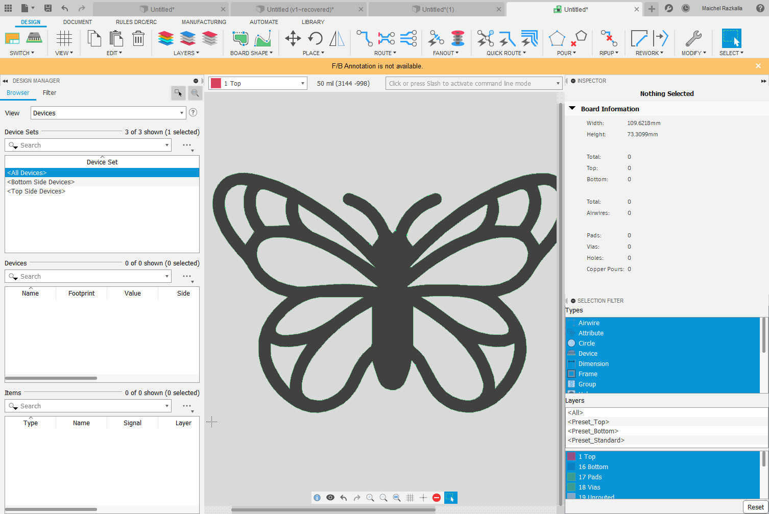
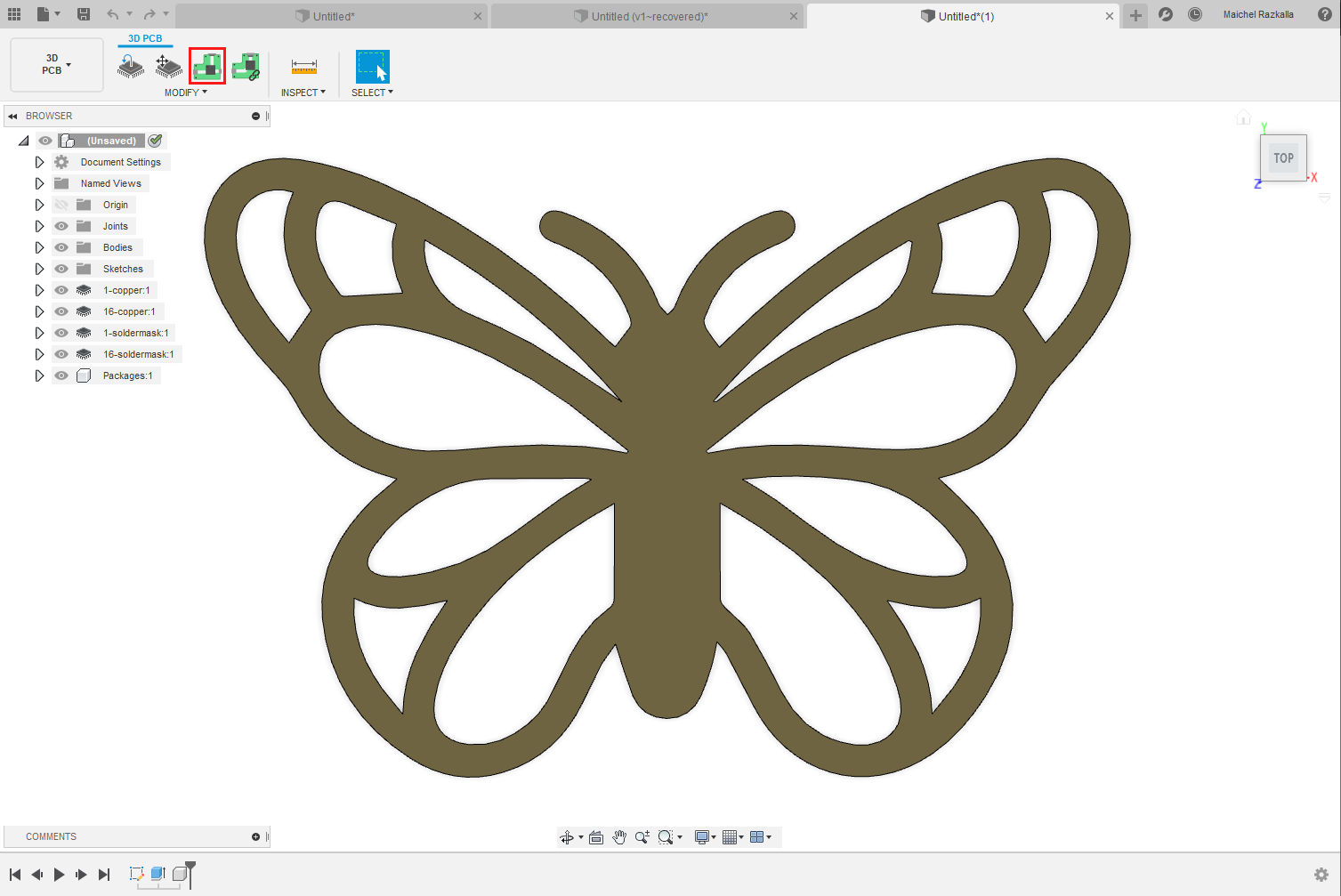
A few weeks later I found that eagle is much easier to make the PCB I exported that I have finished in fusion 360 and imported it in eagle so to finish everything faster.
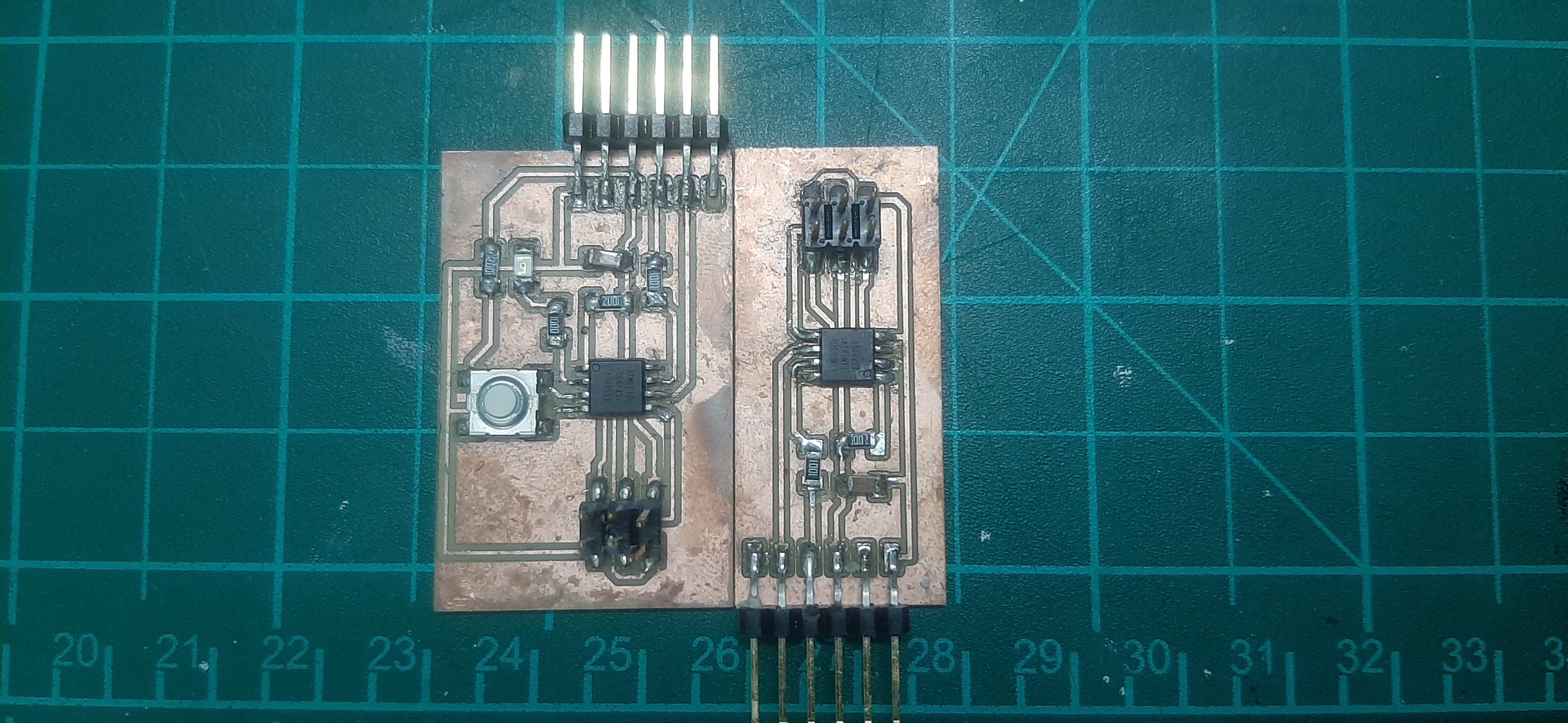
This PCB consumed a lot of time to finish but I’m very happy with the final results
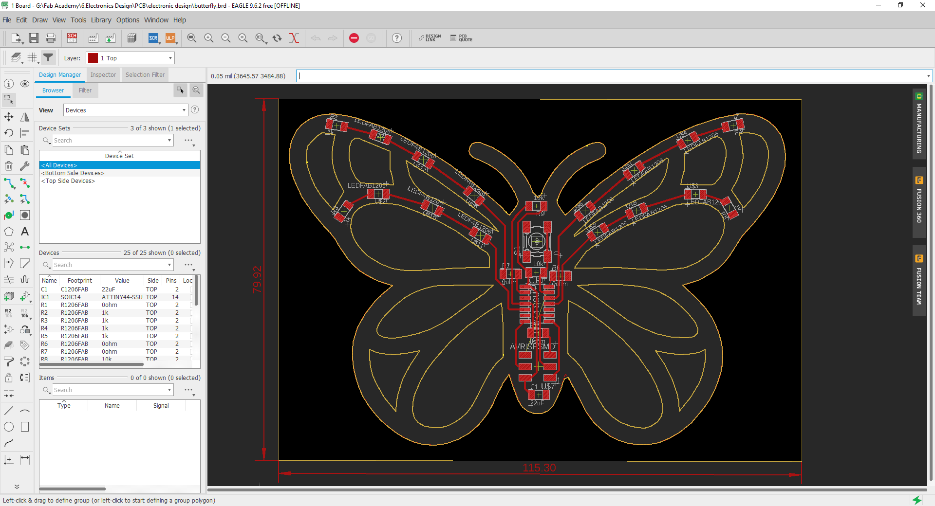
To make this PCB I followed the last PCB steps but there was a problem with PCB layout first time failed because it cut the PCB layout first and that started to cut the butterfly wing holes and that makes the PCB move and round the hole PCB
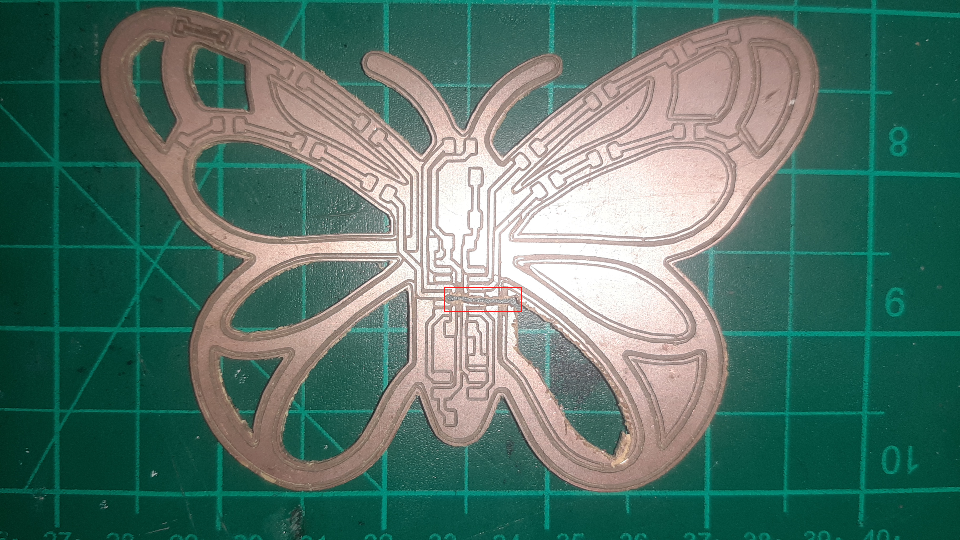
So I used gimp to make 2 layout cut first will be the butterfly holes second step is to cut the outer PCB and finally, I have the PCB

After cutting and soldering the PCB this was the final result.
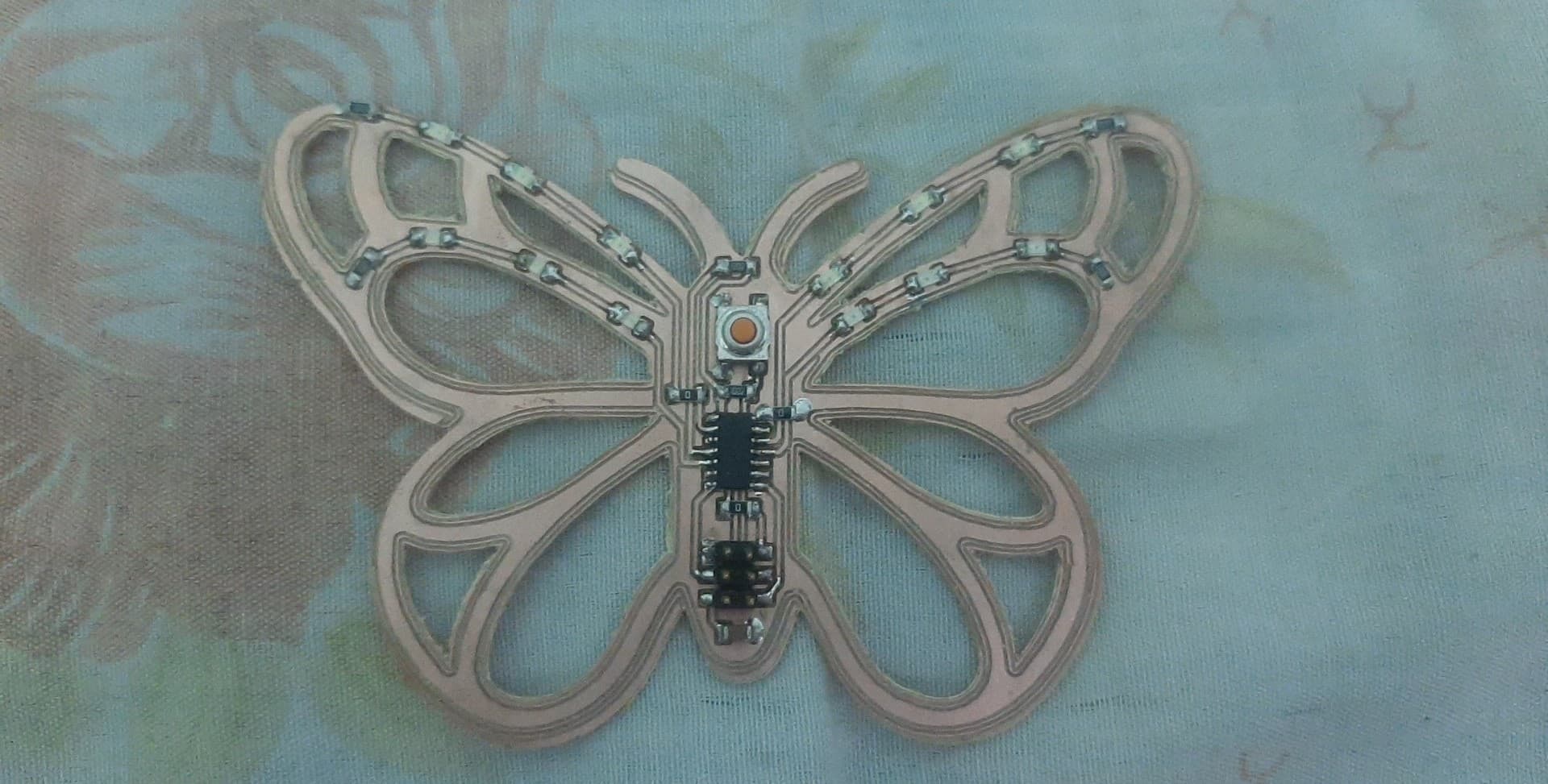
So because this week was very long I will program this PCB with the pushbutton PCB in the embedded system assignment.