Electronics Design
What’s going on?
This week We gonna design and make some PCBs(Printed Circuit Boards). Simply, PCB is a board that contains some lines(Tracks) and pads that connects the components together and allow the electricity(signals and power) to travel from point to another through those tracks without the need to use any external wires or jumpers.
The goal from this week is to design our own PCB board and fabricate it, The board should be able to read some inputs from a pushbutton for example and write some outputs on some LEDs for example. There are a lot of softwares out there that we can use to design our board like EagleCAD, KiCAD, Altium, ..etc Personally I will use EagleCAD and KiCAD and if I will try to explore designing my board by programming.
What’s the ATtiny44 And It’s Bare minimum Configuration
The ATtiny44 is a microcontroller chip that can get programmed to do execute some commands like blinking an LED or driving some motors or getting data from sensors,
Now we need to know, What’s the bare minimum configuration for this chip to work? The bare minimum configuration means using the smallest possible quantity of components that makes that thing runs without problems. but later on, we will add some more components like LEDs, buttons, pin headers to spice things up.
After looking at Prof. Neil’s “Hello Echo” board and analyzing it, I found that we need:
- 1UF bypass capacitor between the VCC, GND pins.
- 20MHz resonator(or a crystal oscillator with two 22pf capacitors).
- 03x02 AVR ISP connector to be able to connect our board to the programmer board and program it.
- An FTDI connector which allows the board to communicate with the computer through the serial communication (Tx, Rx).
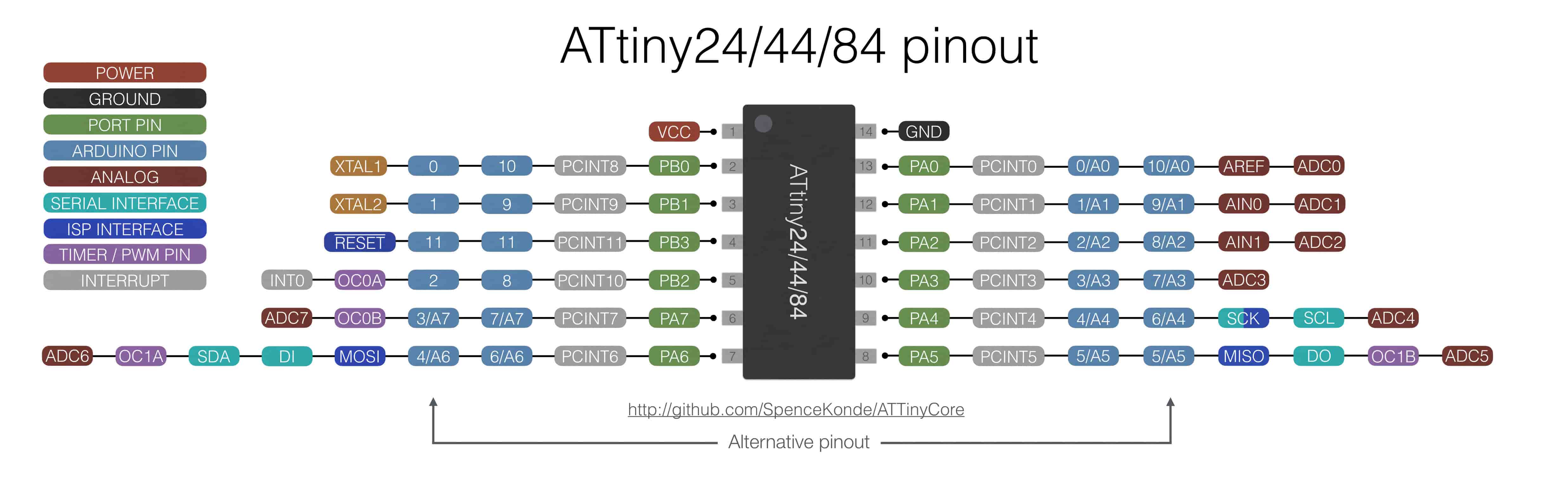
After knowing the bare minimum configuration of the chip, we need to know what’s the pinout of the chip. We gonna use the “Arduino pin numbering” to connect the inputs and outputs (pushbuttons and LEDs) on them, also we gonna use the Arduino numbering in the programming part too.
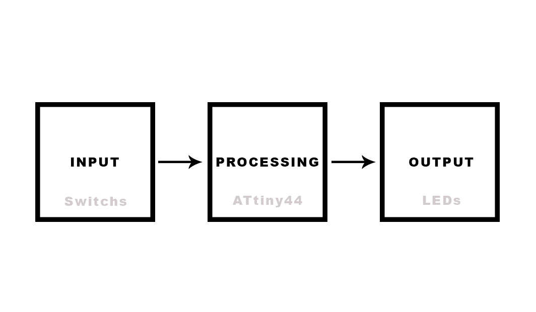
Before start working on the schematic design, let’s list the functions that we need our board to serve and according to that functions we gonna list also the components that we will need to use in the schematic design to help us achieve these functions.
- The board should be able to read inputs from the pushbutton.
- The board should be able to turn the LEDs on and off depending on the pushbuttons readings.
The Used Electronic Hardware
| Part Number | Description | Quantity |
|---|---|---|
| ATTINY44A-SSU-ND | IC AVR MCU 4K 10MHZ 8SOIC- | 1 |
| XC1109CT-ND | CER RESONATOR 20.00MHZ SMD | 1 |
| S1143E-36-ND | SMT RT Angle Male Header 0.1" (36pos) | 1 |
| 609-5161-1-ND | 6 Positions Header Connector 0.100" SMD | 1 |
| 445-1423-1-ND | CAP CER 1UF 50V X7R 10% 1206- | 1 |
| 311-10.0KFRCT-ND | RES 10.0K OHM 1-4W 1% 1206 SMD | 3 |
| 311-4.99FRCT-ND | RES 4.99 OHM 1-4W 1% 1206 SMD | 2 |
| B3SN-3112P | SWITCH TACTILE SPST-NO 0.05A 24V | 2 |
| 160-1169-1-ND | LED Orange CLEAR 1206 SMD- | 1 |
| 160-1169-1-ND | LED White CLEAR 1206 SMD- | 1 |
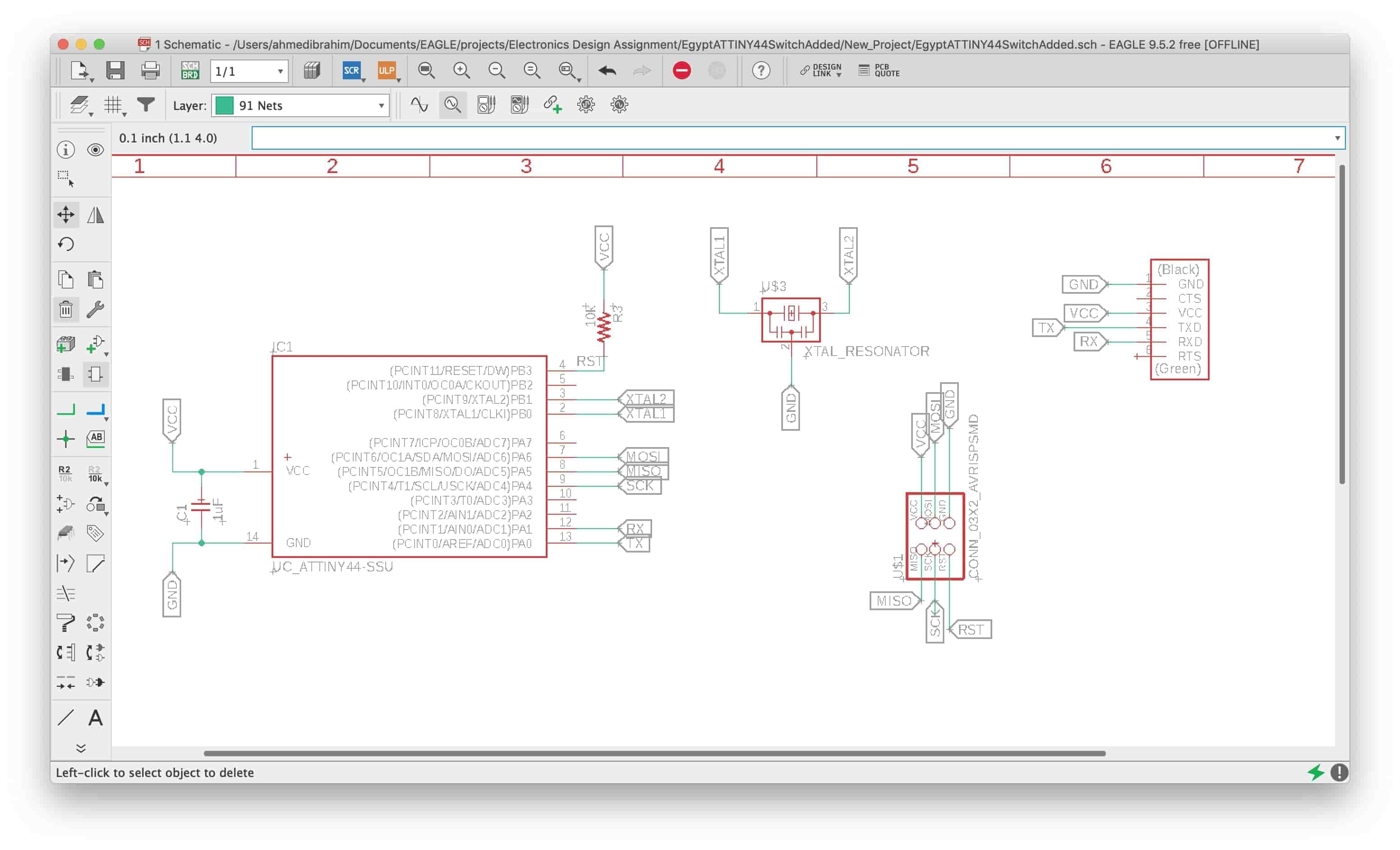
Using EagleCAD to design the Circuit
After sketching and planning specifically what do we wanna achieve this assignment, let’s open EagleCAD and start designing. Actually, I have some experience in electronics and PCB design using EagleCAD and KiCAD.most of my previous designs are based on THT, I designed only one SMT board in “Electronics Production week” I designed a simple LED blinking That’s why I’m very excited to design my second SMT board.
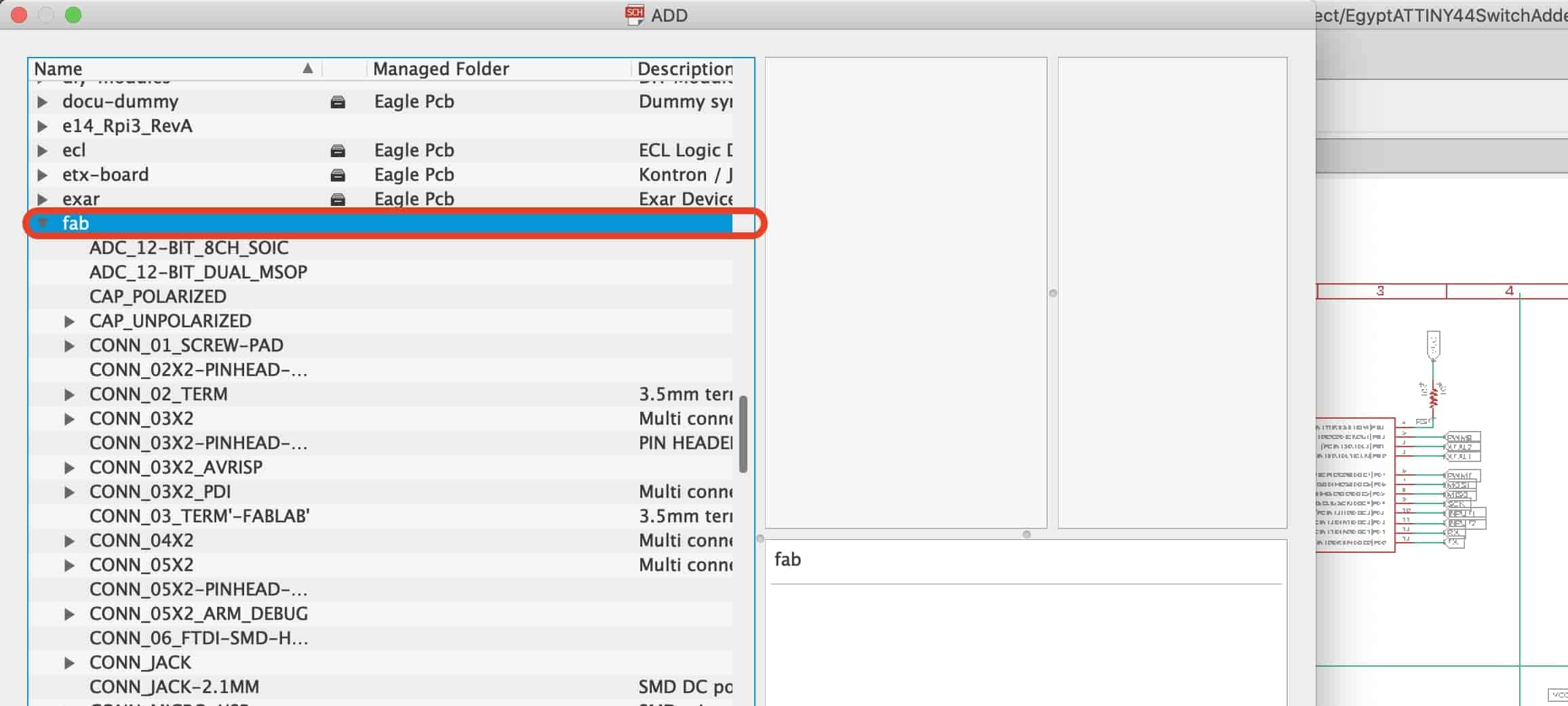
- Add the Fab Library.
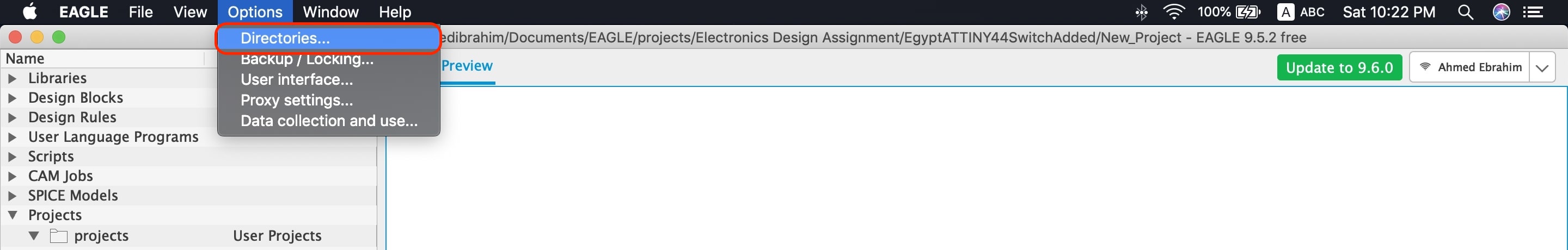
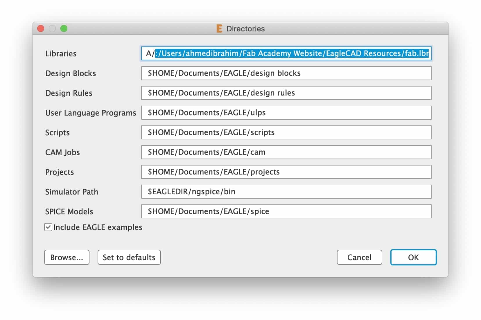
After downloading the Fab Library, I open EagleCAD, from the “Options” menu in the toolbar choose “Directories”.
add a colon (:) after "$EAGLEDIR\lbr", and paste the Fab EAGLE Libraries directory location after that. (If you are a Windows user you should put a semicolon (;) instead of a colon).
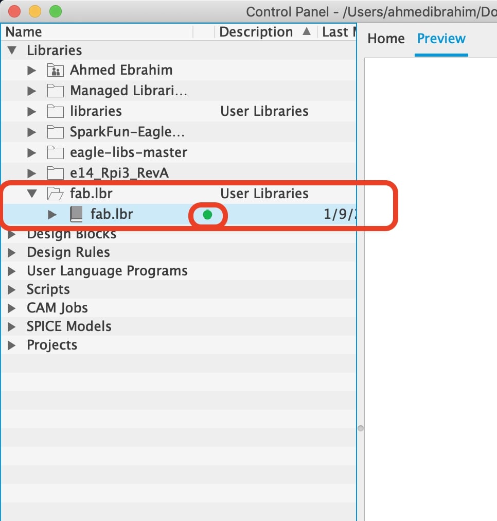
Then From the libraries tab, select the fab.lbr library and activate it by pressing on that small circular button next to it, it should get green after you pressing it which means it’s now activated.
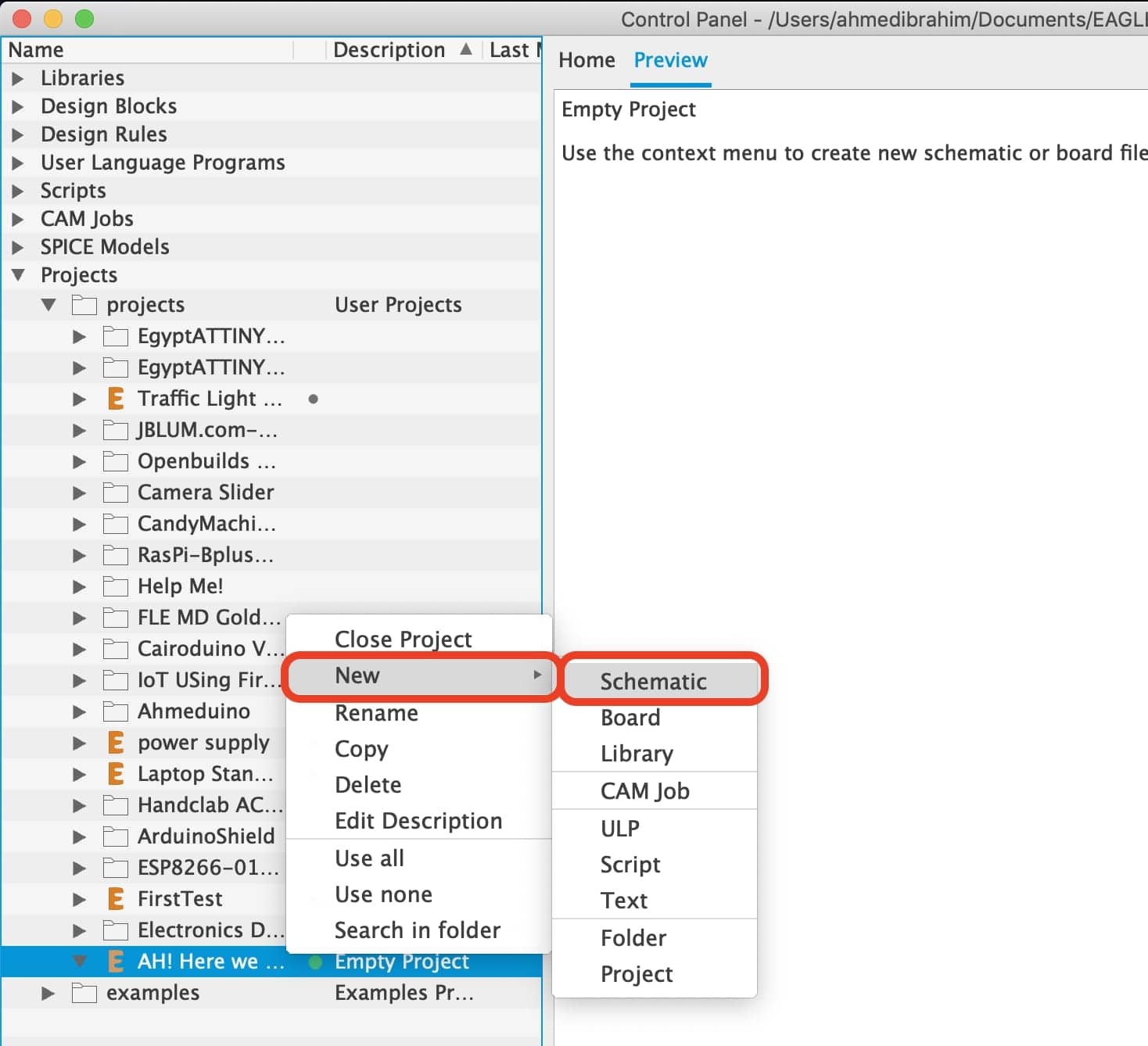
- Create a new project.
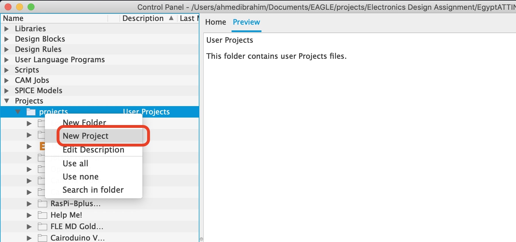
Create a new project by pressing right-click on the “project“ folder, then select “New Project”, then from “New” select “Schematic”
- Start designing the schematic.
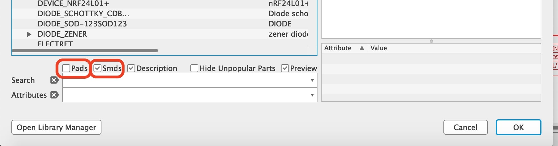
Now, It’s time to add the components that we gonna use to the project workspace, from the “add” tool scroll down till you find the “Fab library” then choose the components.
We can search for the component by its name, to make the searching process easier, since we are using only SMD components we can filter the search results to get results for the SMD components only by checking this box and unchecking these two boxes.
We gonna add all the components that we need in our schematic workspace before making any connection between any of them.
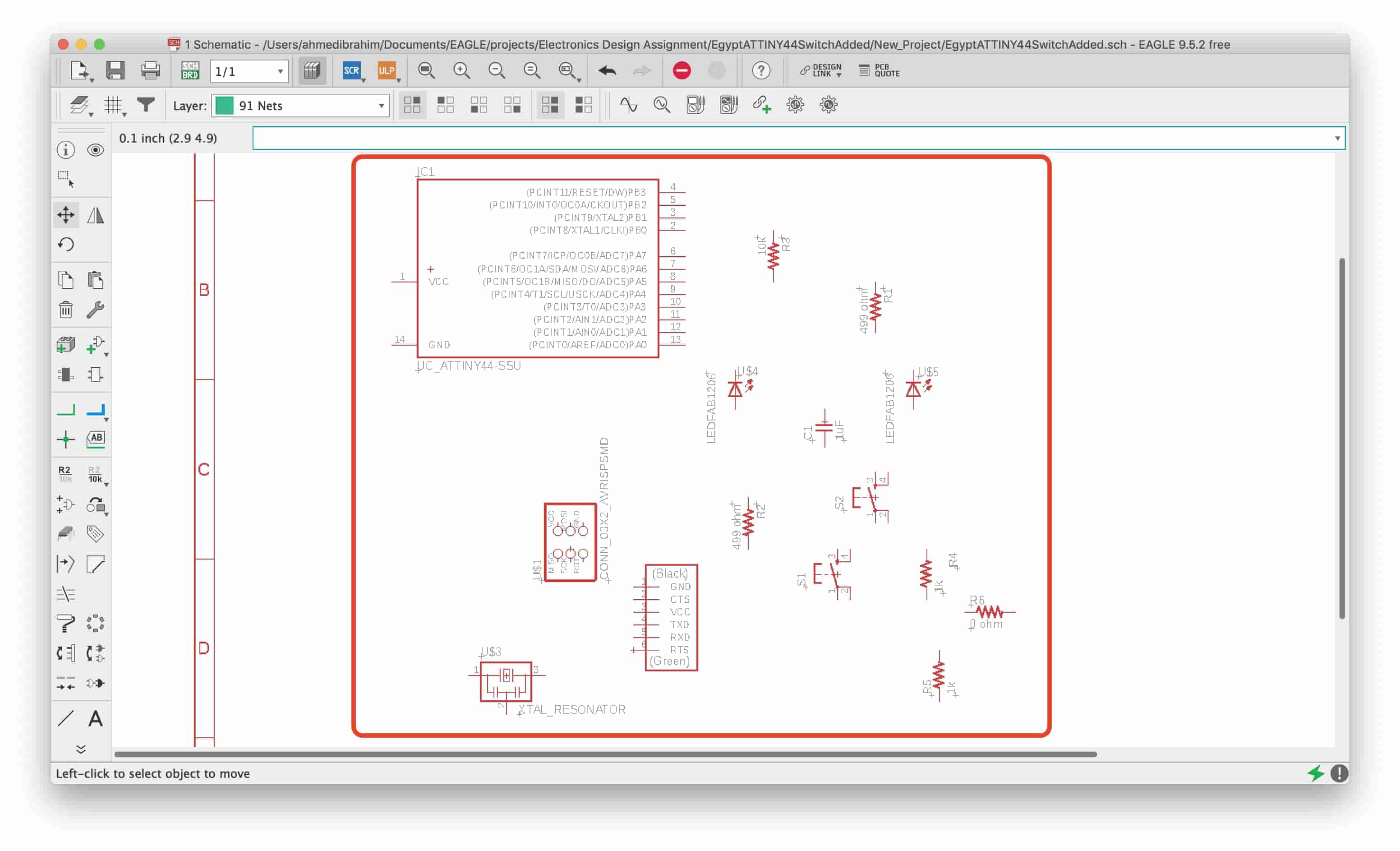
To move components around we can use the “Move” tool from the left-side toolbar, we gonna organize our workspace to make things easier.
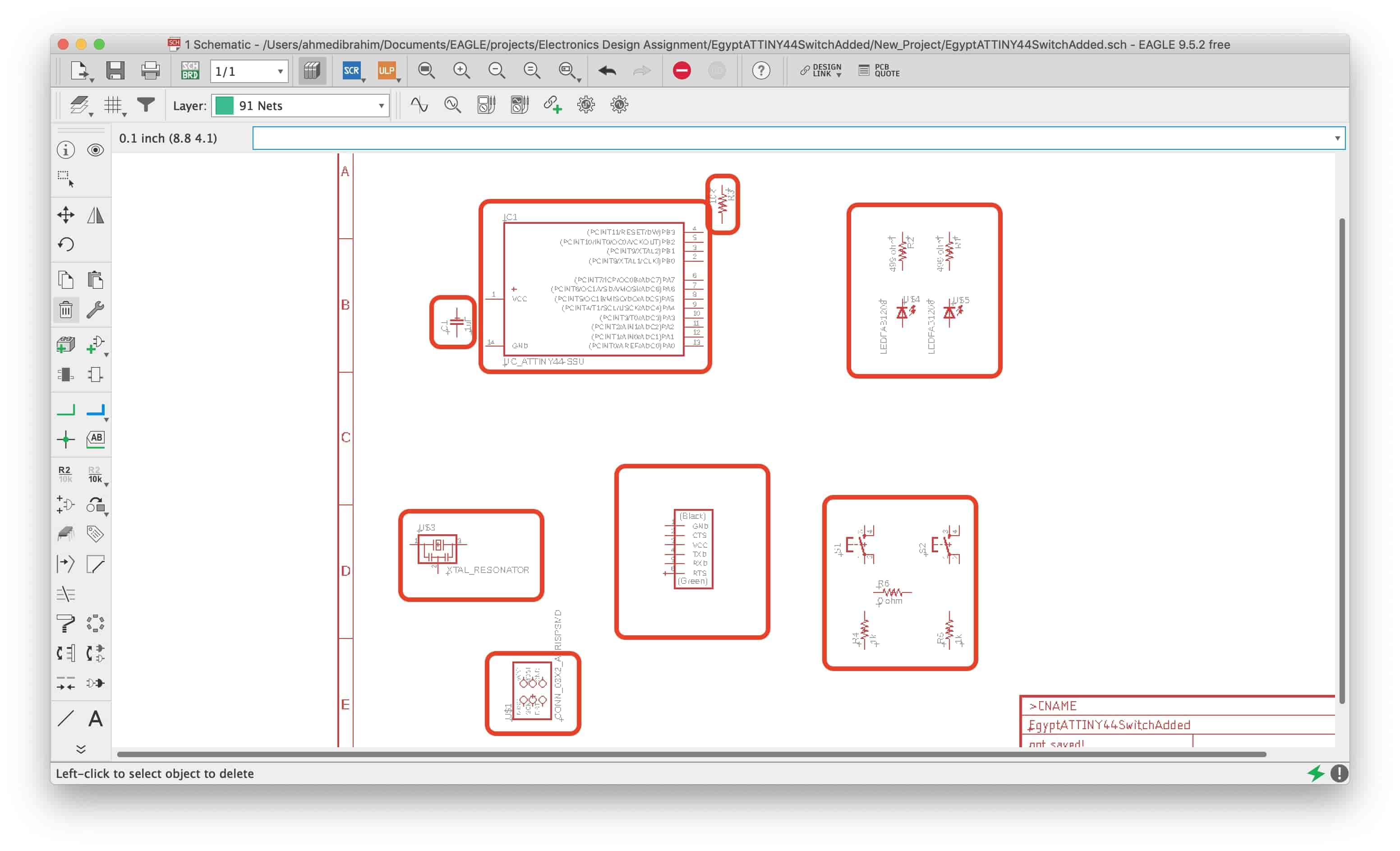
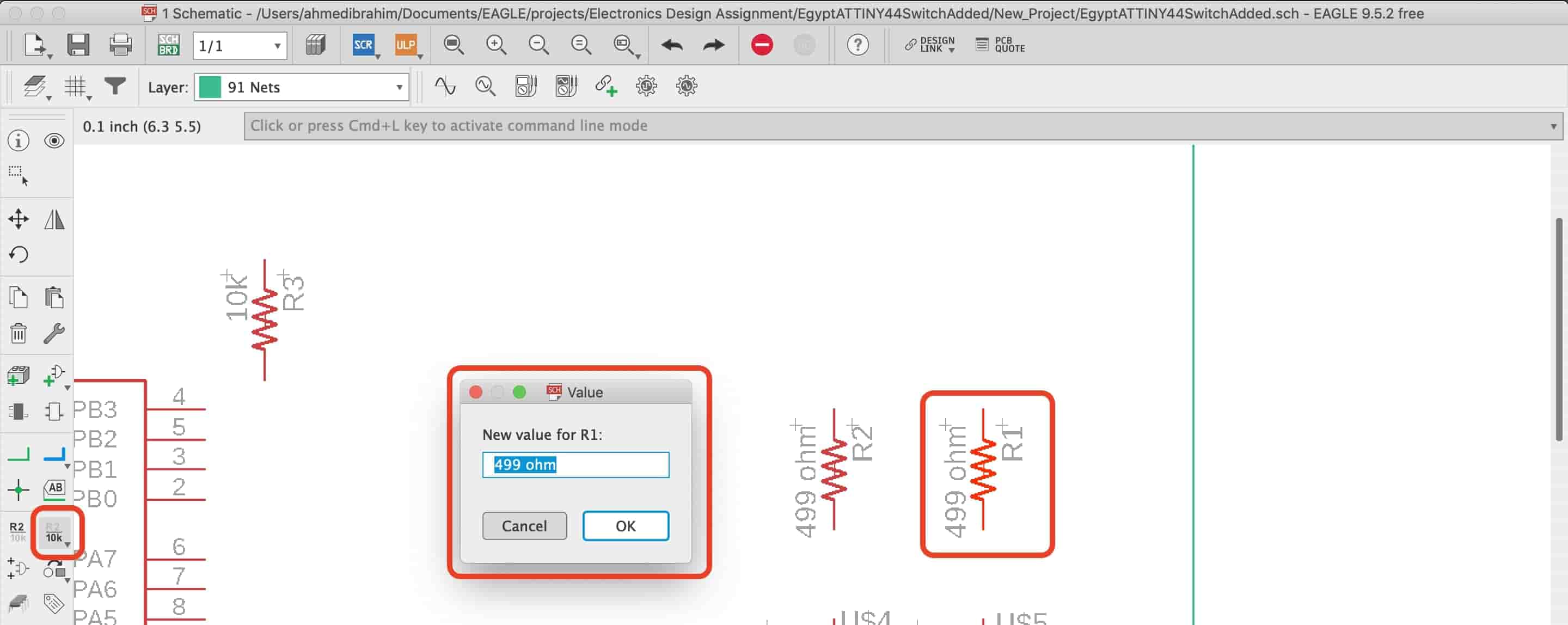
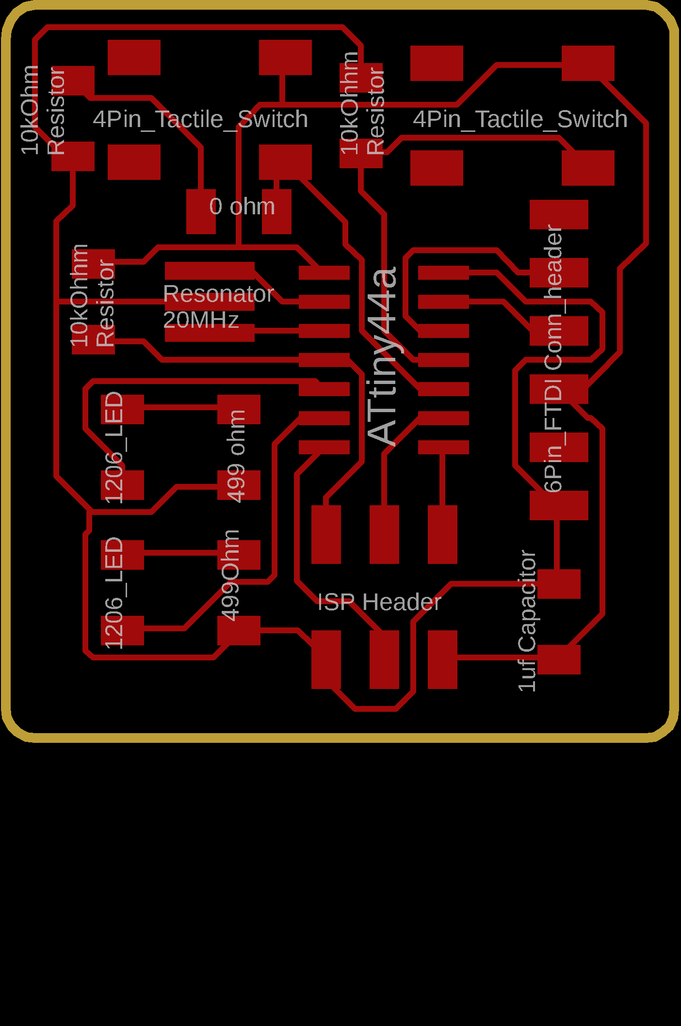
Now we gonna give each component a value like we gonna use a bunch of resistors each one should have its own value(in ohms), the same with capacitors and any other component that should have a value.
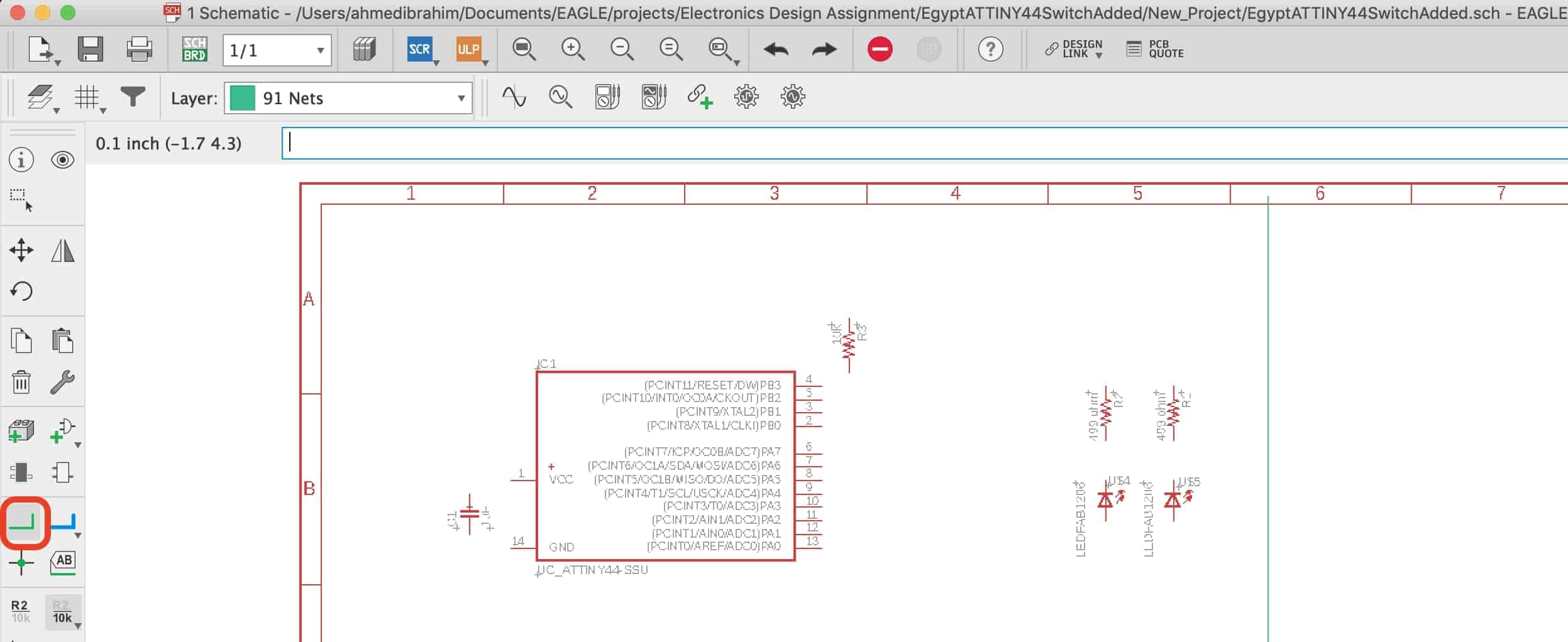
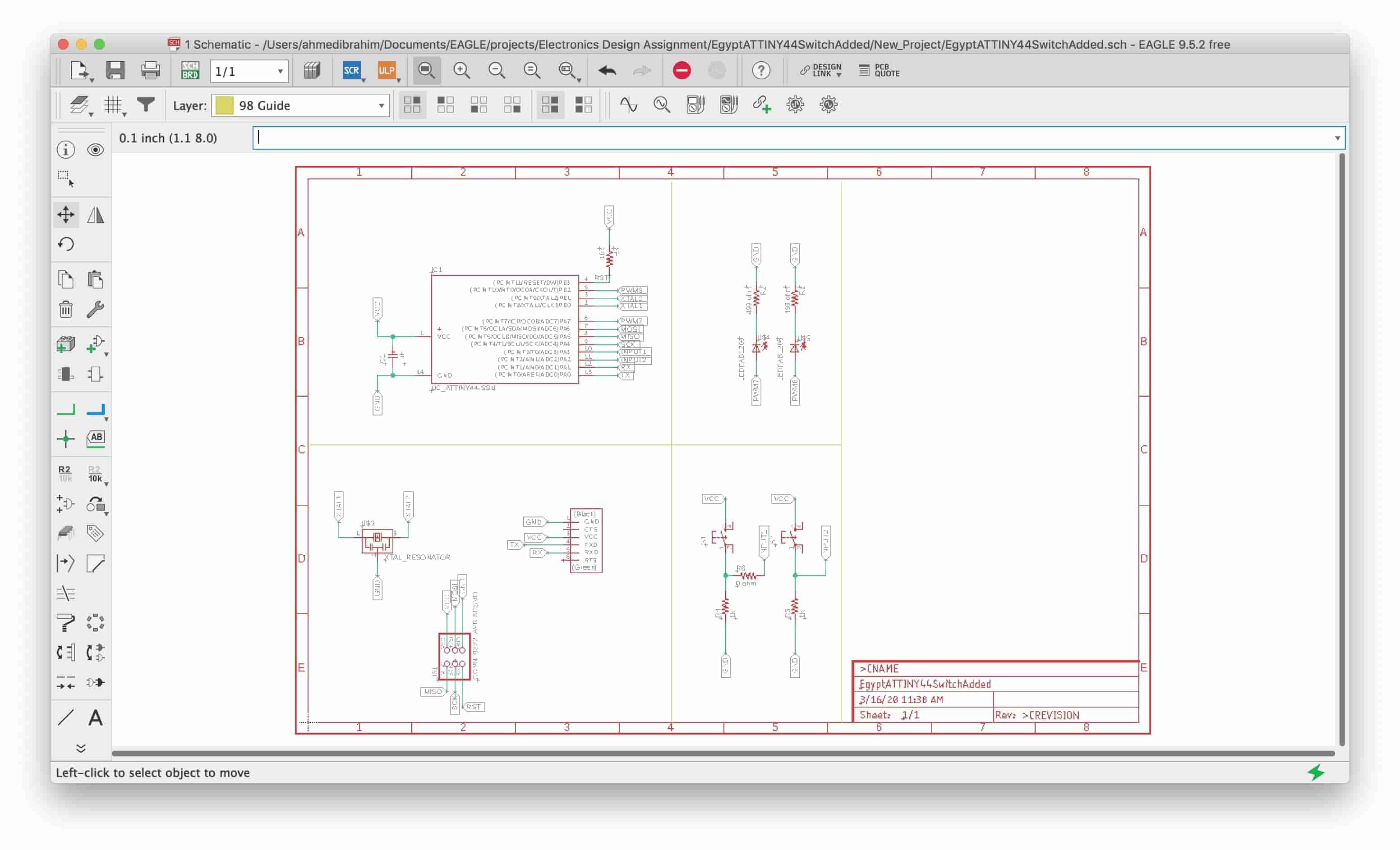
After stuffing all the components that we gonna use, now it’s time to connect things together. To do that we gonna use the “Net” tool to connect between any two points. Later on, these nets will get translated into tracks in the PCB layout.
- Switching to the PCB layout.
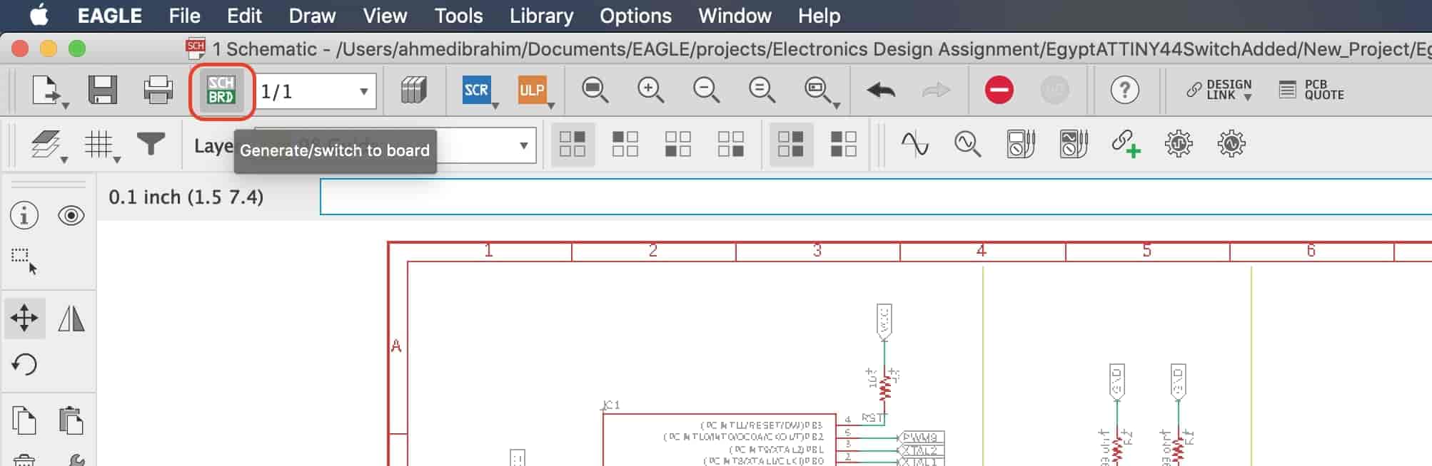
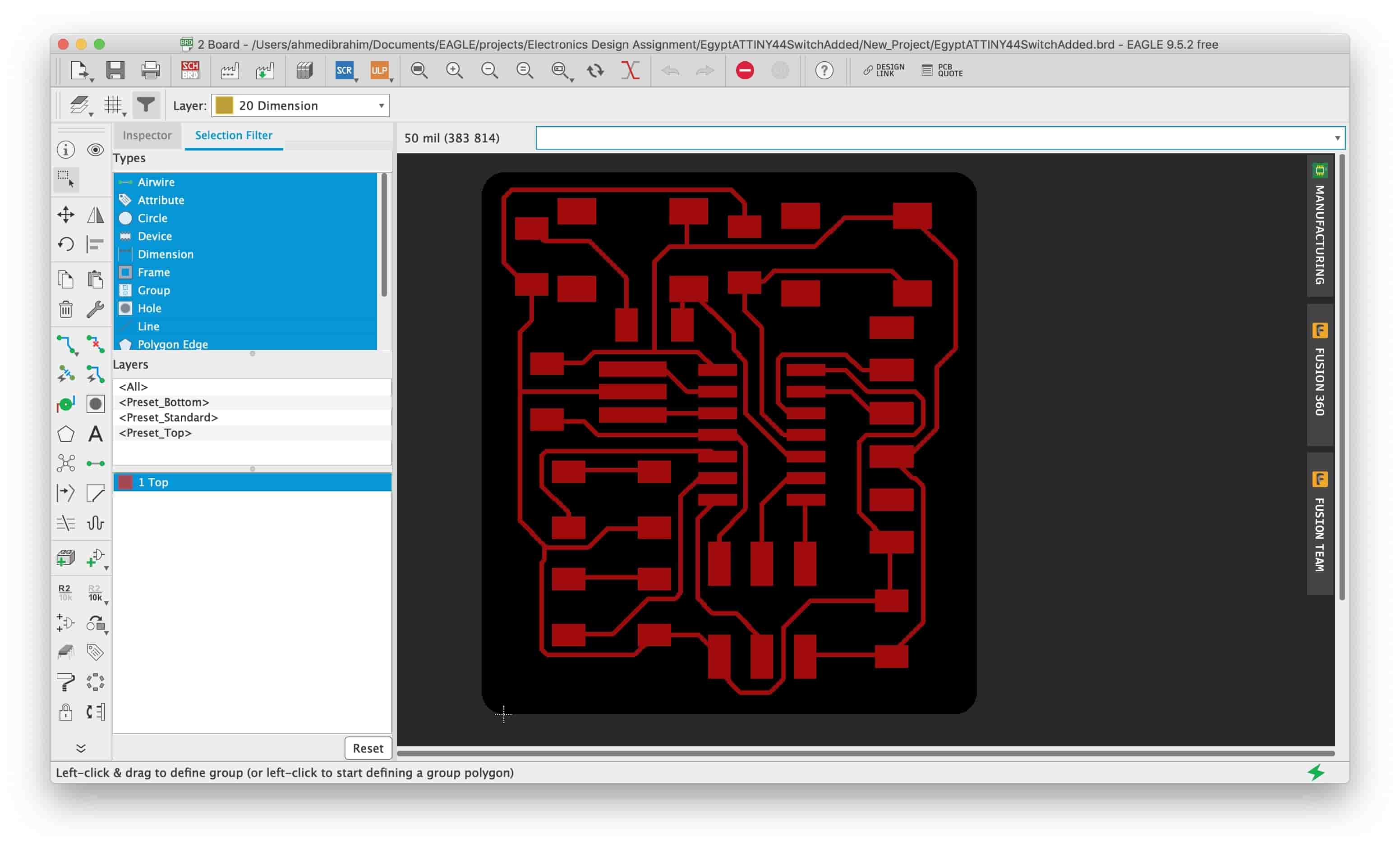
Yaay we finished our circuit schematic, now we need to draw the PCB board layout. To switch to the PCB layout file we need to press that “Switch/Convert PCB layout” button. It will open that page.
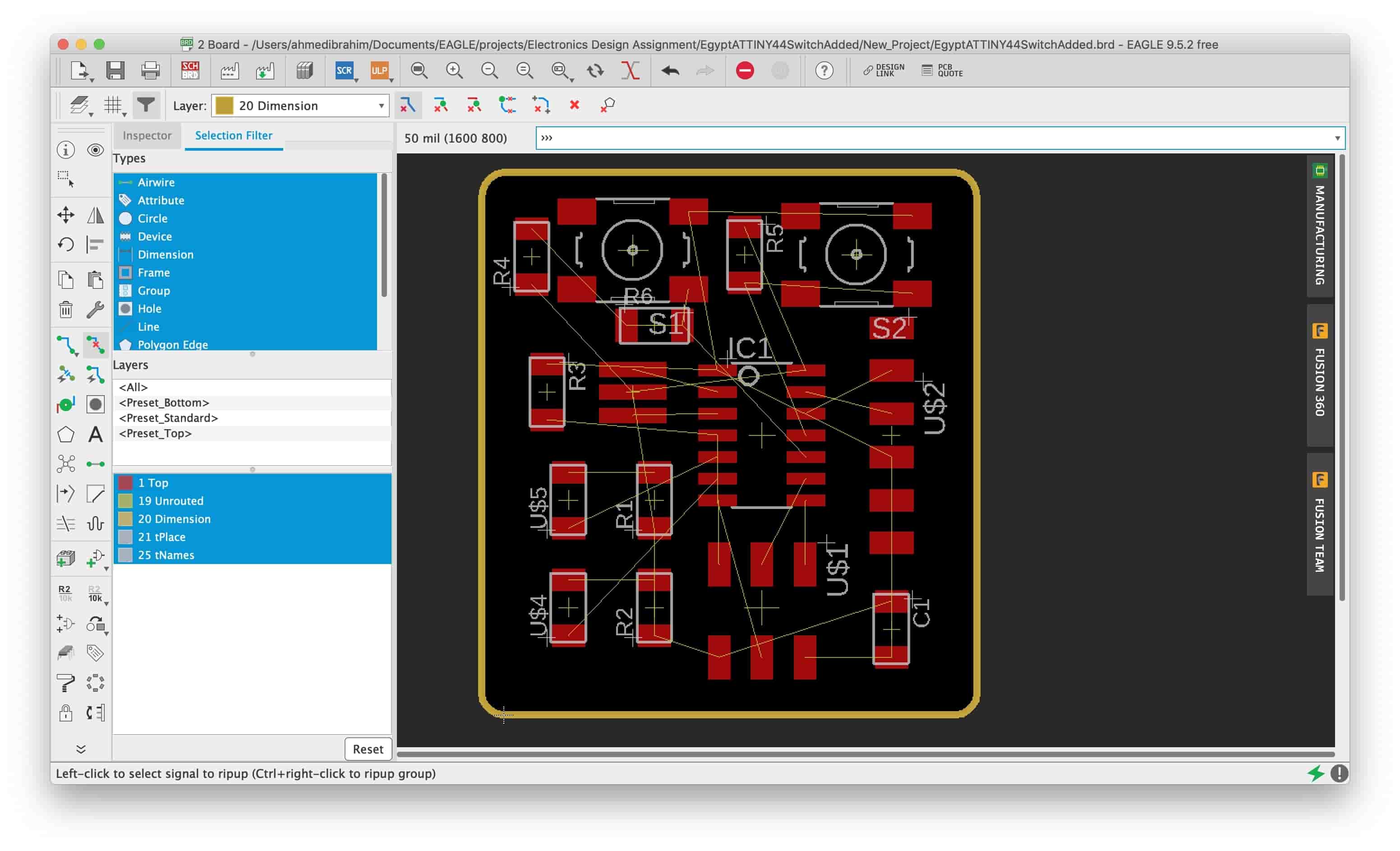
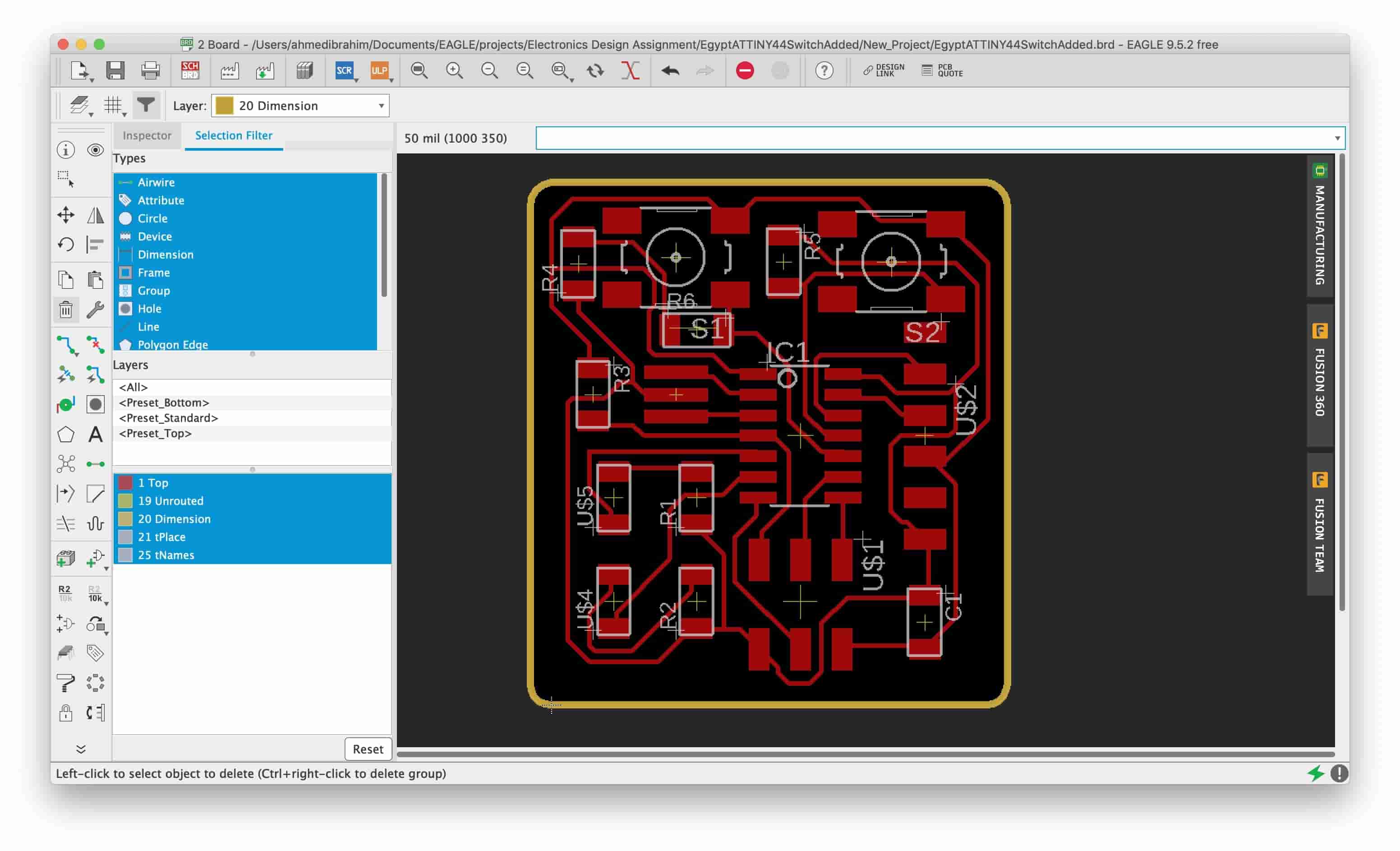
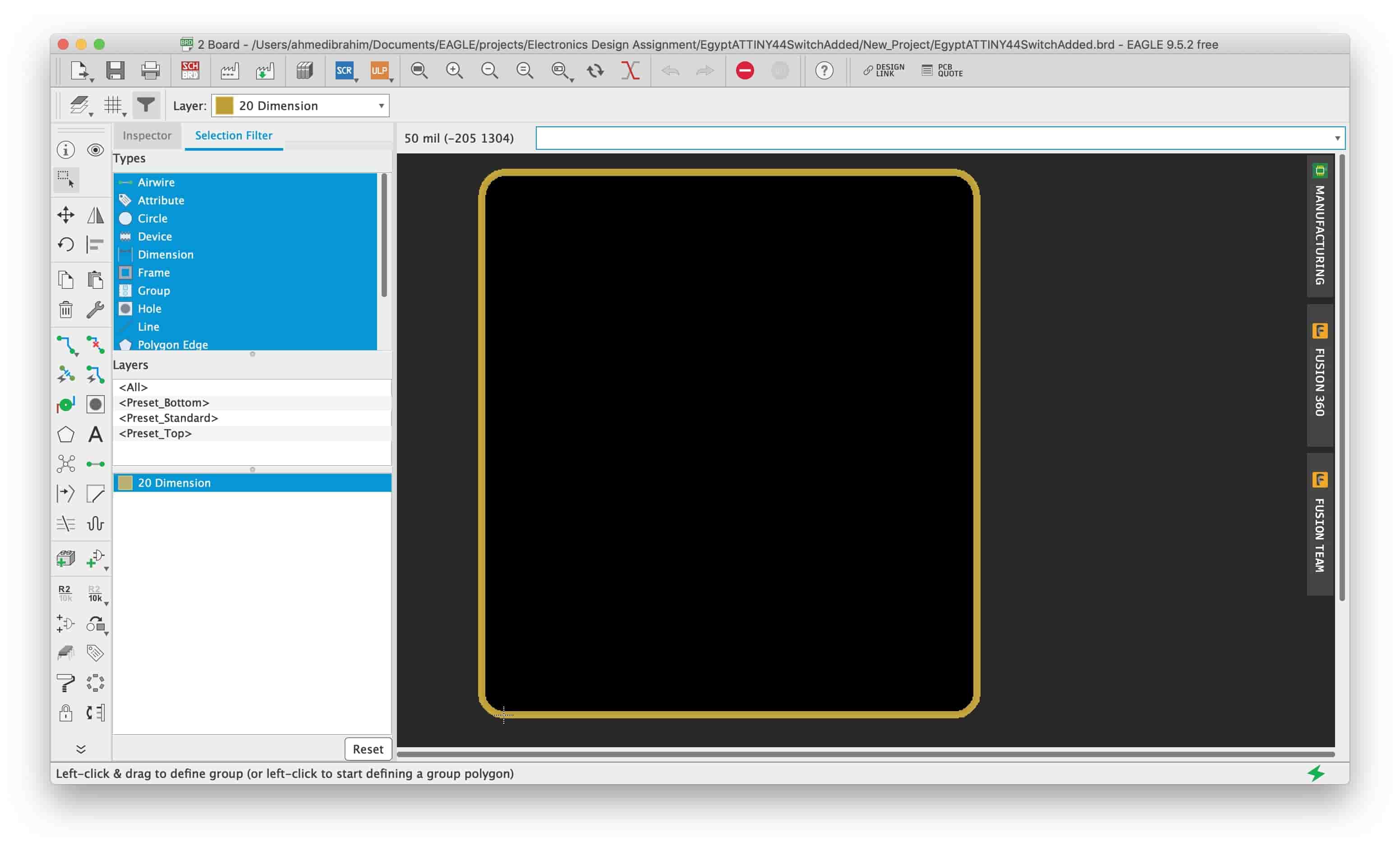
Now, we need to move all the components inside the PCB profile and organize all the relevant components near each other, which will make the routing process easier.
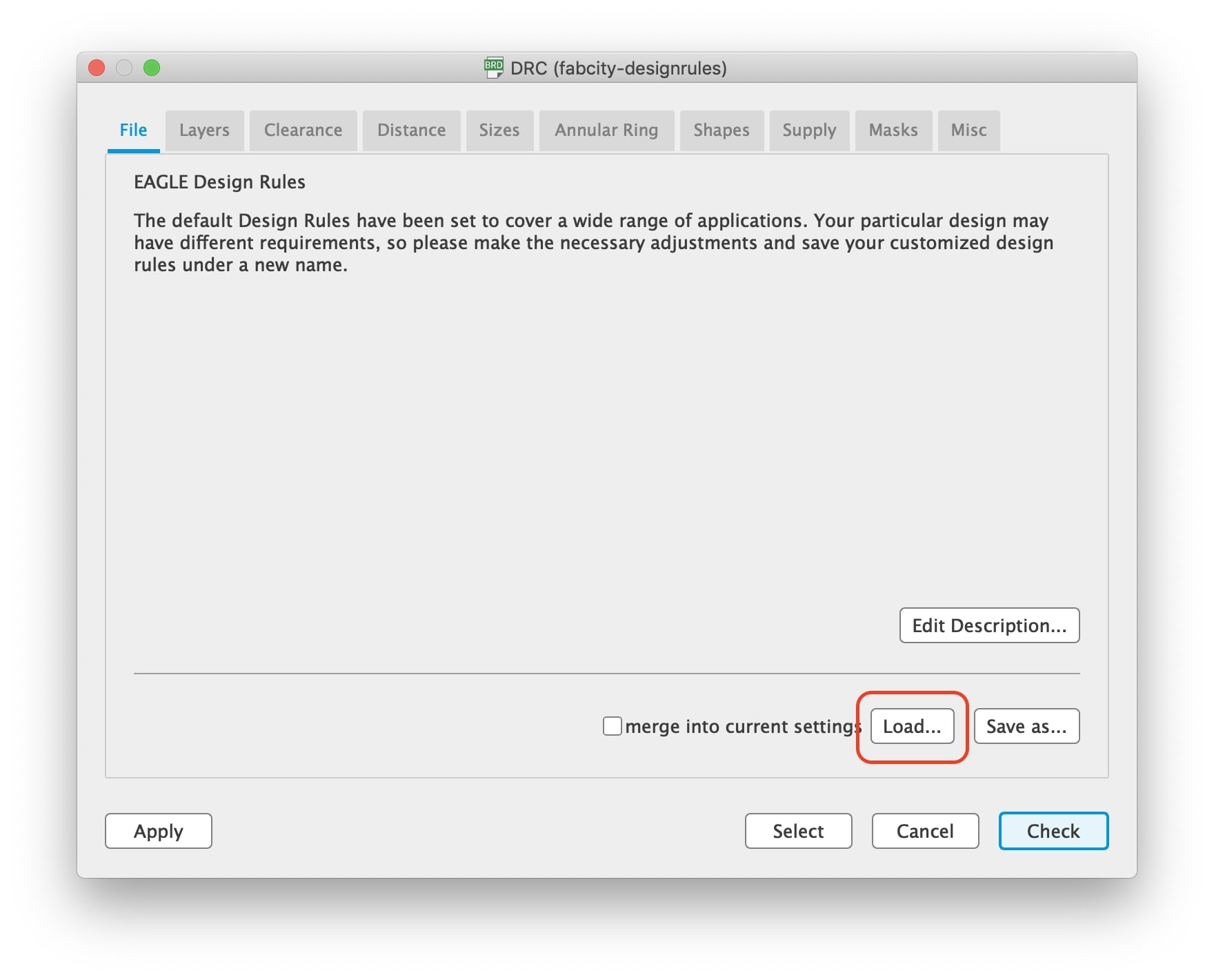
Now, we need to set some design rules. Design rules define all the parameters that the board layout has to follow, sets of rules for things like spacing between board features and minimum sizes that all correspond to the tolerances and capabilities of a board manufacturer. Since we gonna fabricate our board on the awesome modela in the Fablab, we can load the Fablab design rules files instead of setting all of these parameters manually.
Now, we have two options, the first option is to use the “Autorouting” tool which tells the program “Yo Dude! I’m lazy rn can you make the routing for me, PLZ”. The second one is to make the routing process manually by yourself and it’s a professional and more efficient way.
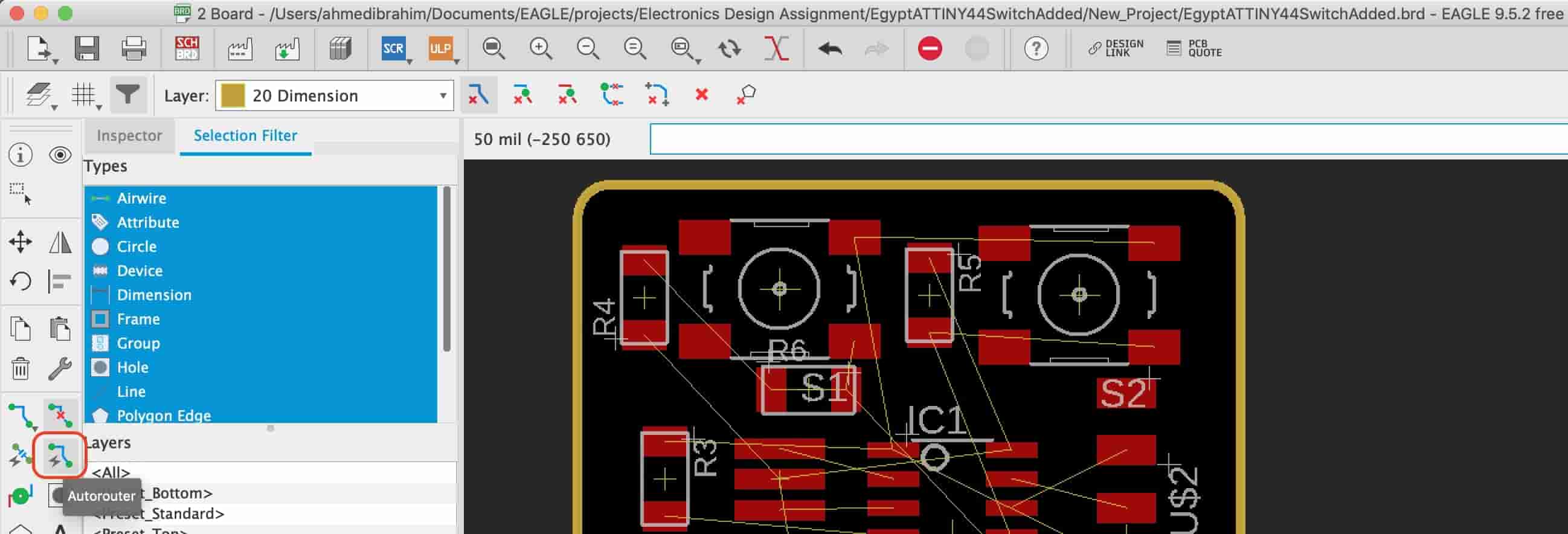
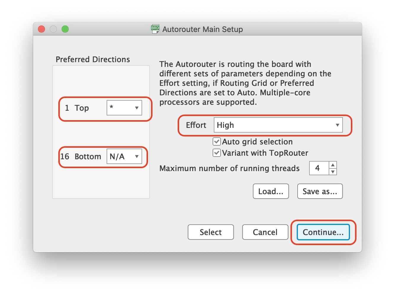
We need to tell the autorouter to route the board on the top layer only with high effort.
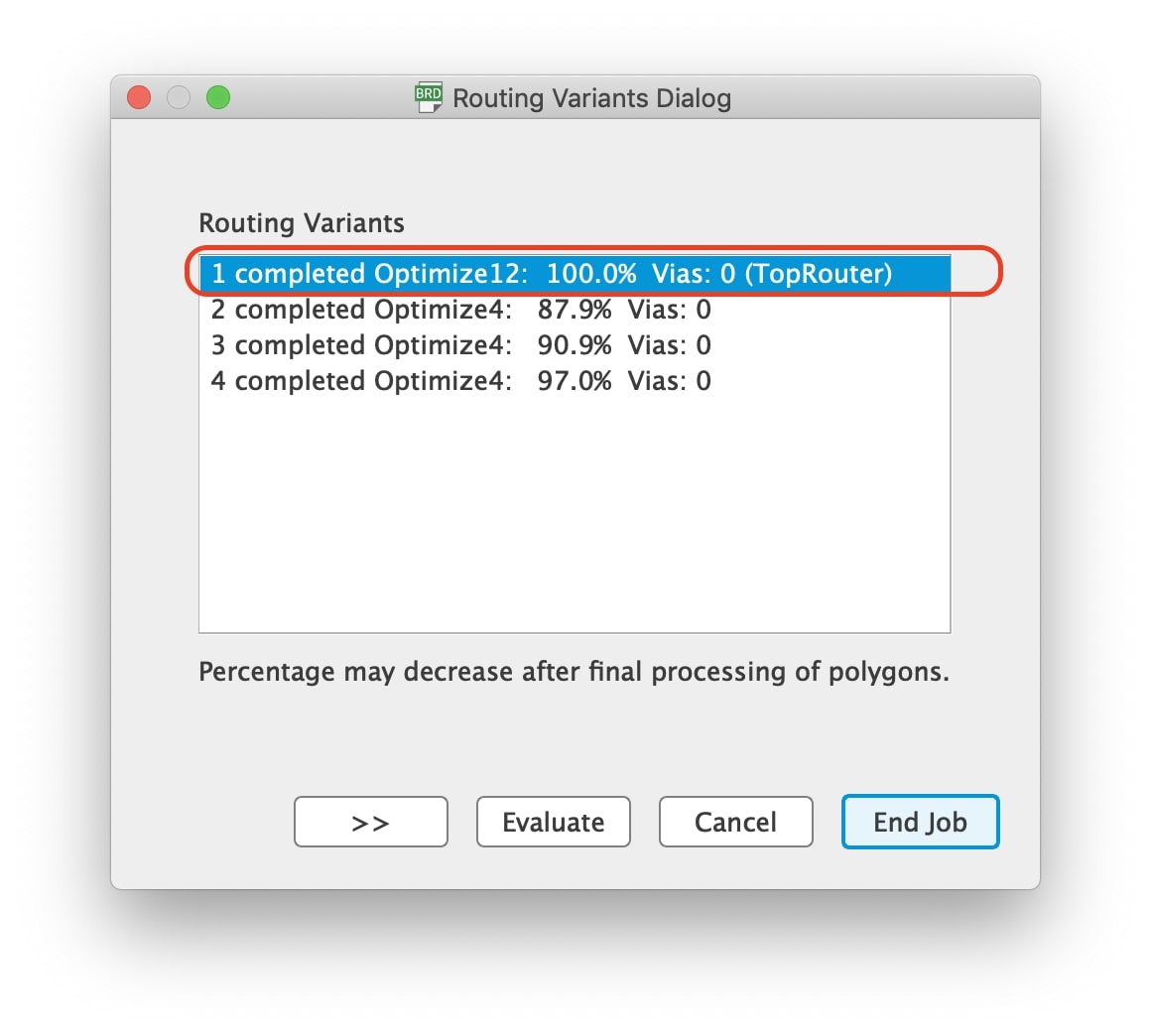
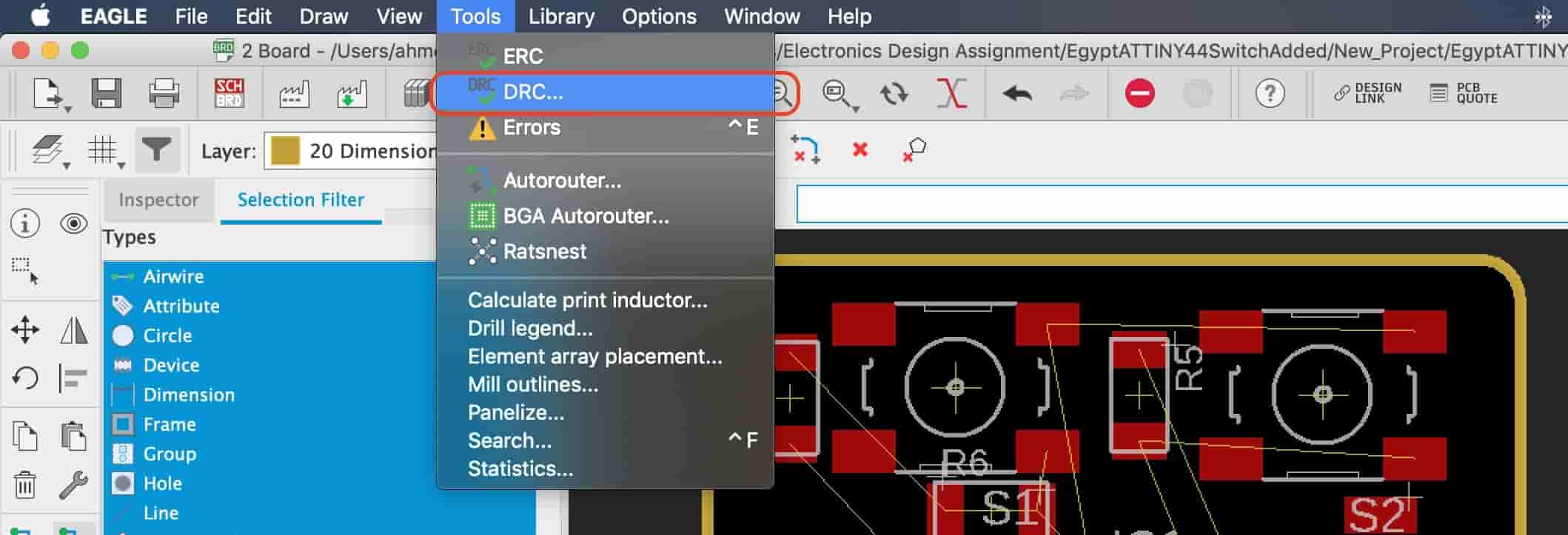
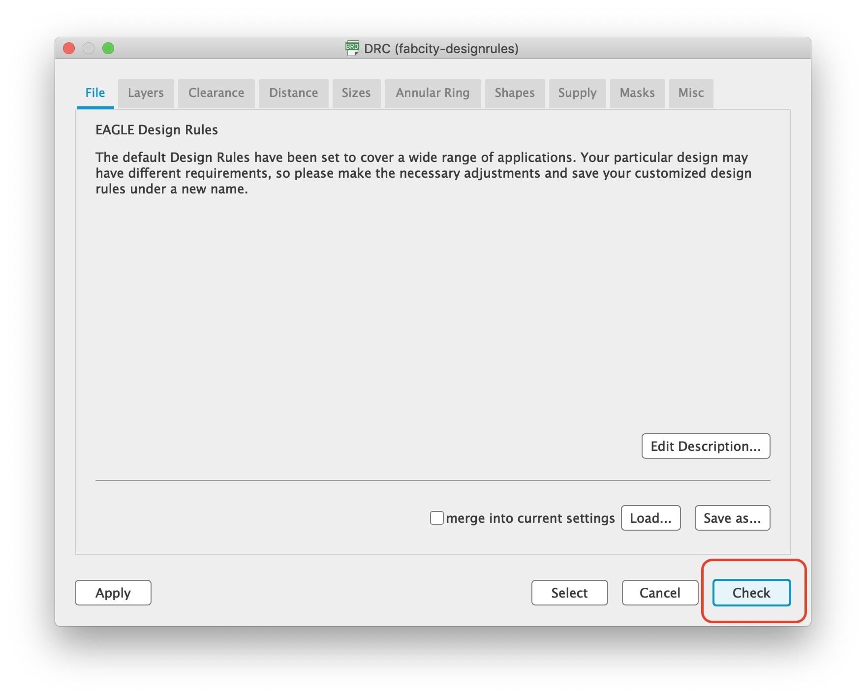
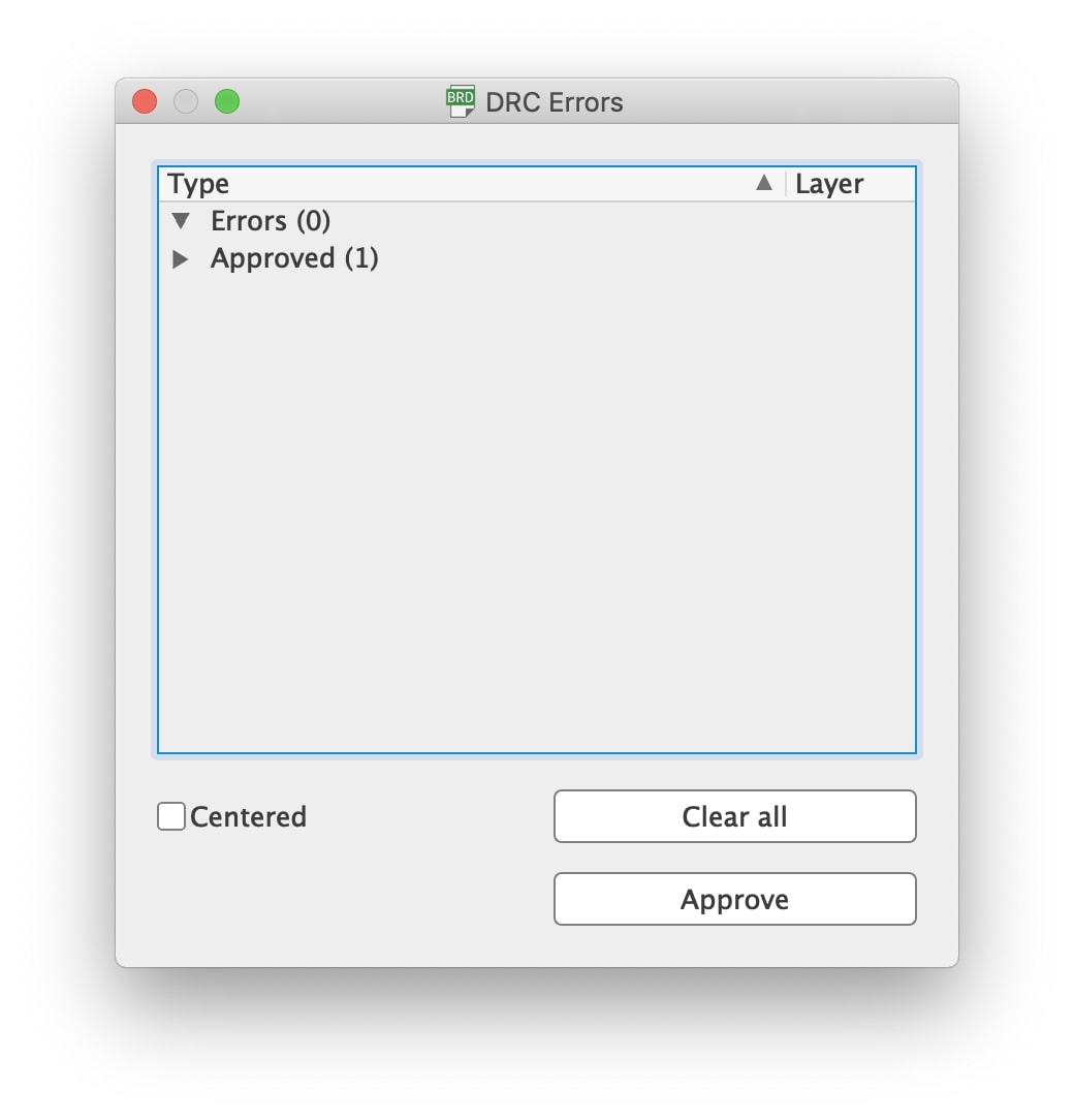
After finishing the routing process, let’s check if there are any errors in my layout(clearance, track size, overlapping) we need to open the “DRC” tool and click the “Check” button.
We have no errors. At this step, we have finished the board schematic and PCB layout. We should be ready for manufacturing.
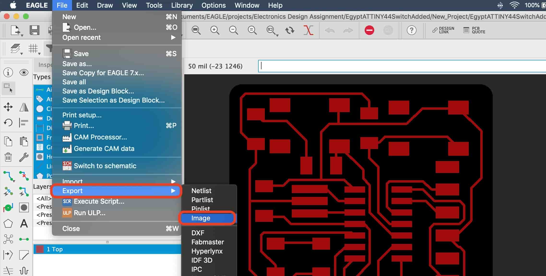
Exporting Fabrication files(MAC USERS).
At this point, we have finished our circuit schematic and the PCB board layout.
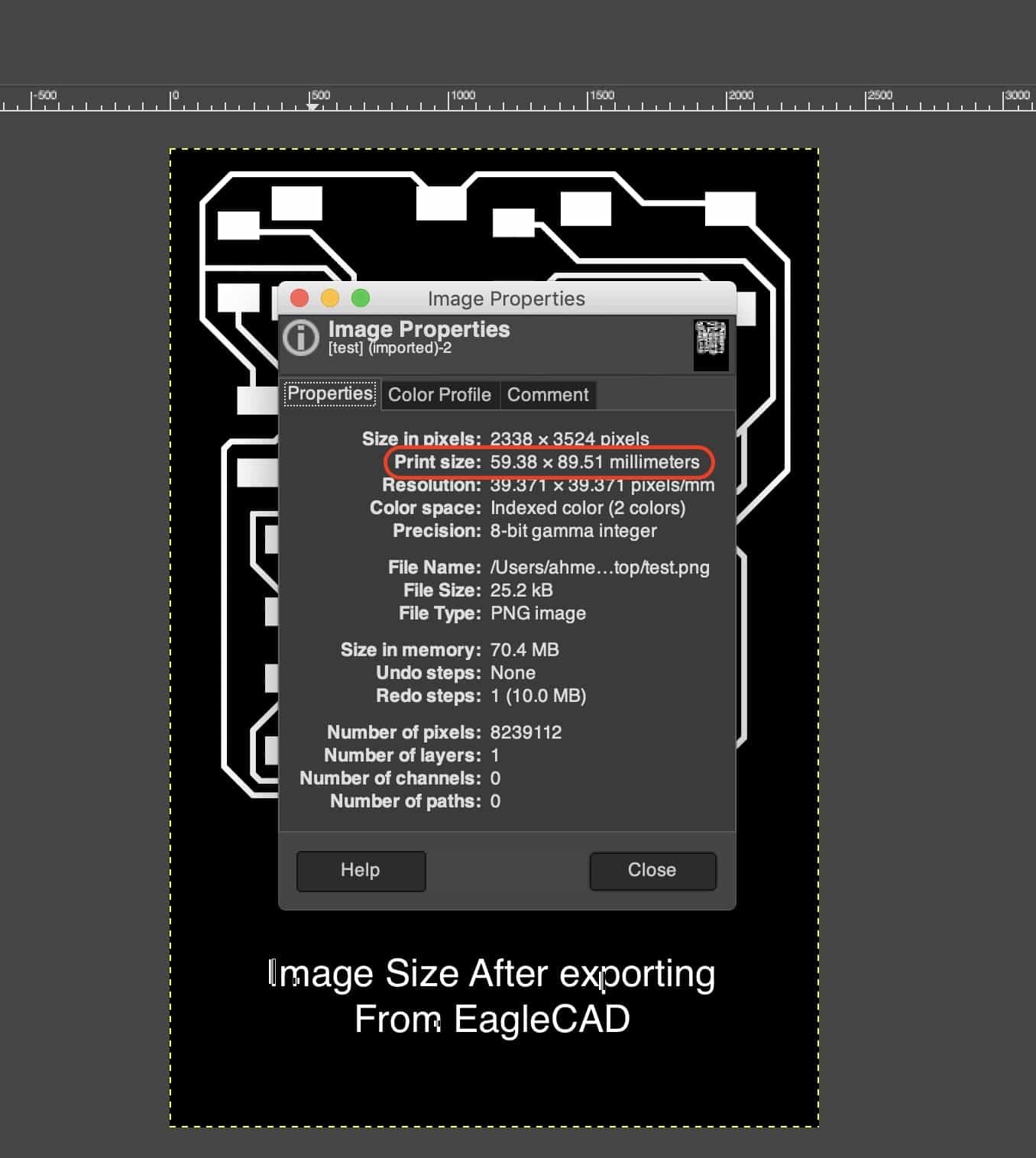
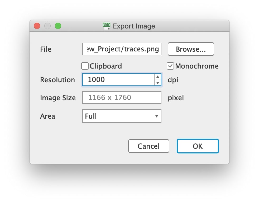
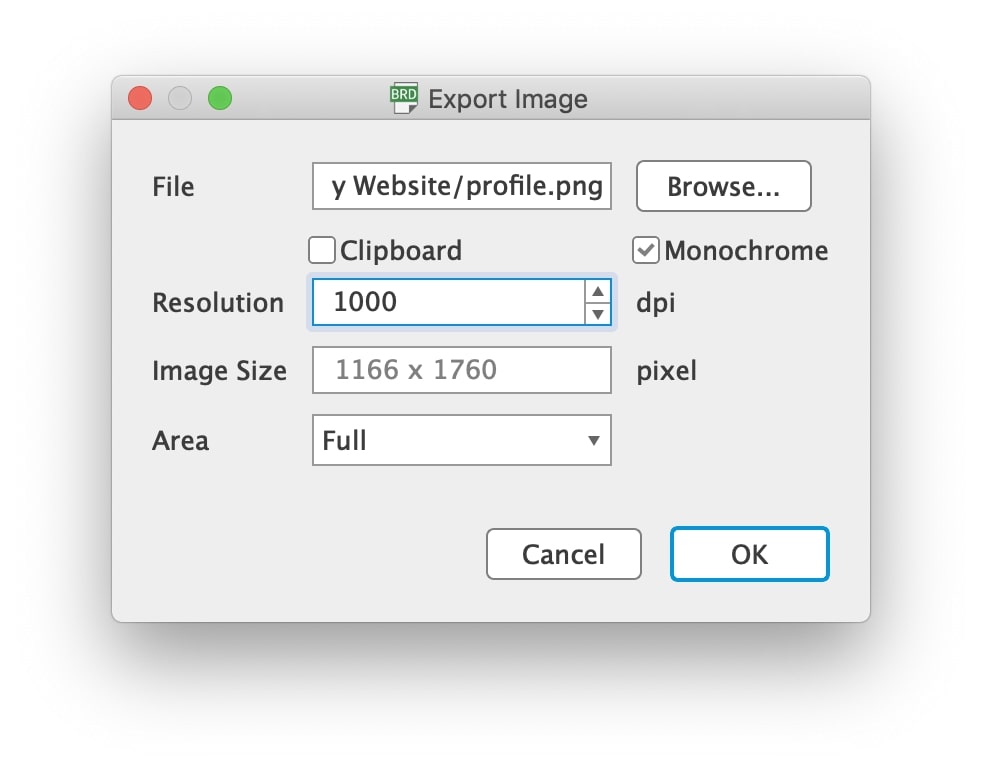
Actually, I was exporting the fabrication file(PNG for PCB traces & another PNG for PCB profile) from eagle using the most popular and known way. From file menu -> Export -> Image. Then I set the DPI to 1000 and the image to monochrome. Easy!
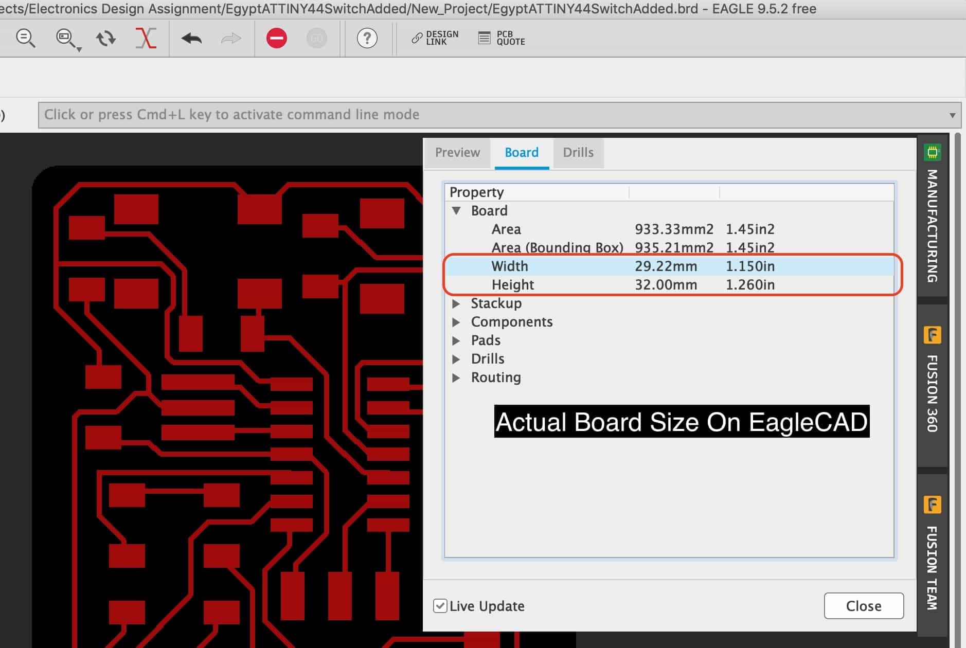
But I faced a huge problem, the output dimensions of the PNG images are not the same dimensions as the actual board. That causes the machine to ruin my PCB many times till I recognized that there’s a mysterious problem in image exporting in the MAC version of the EagleCAD program. Weird!
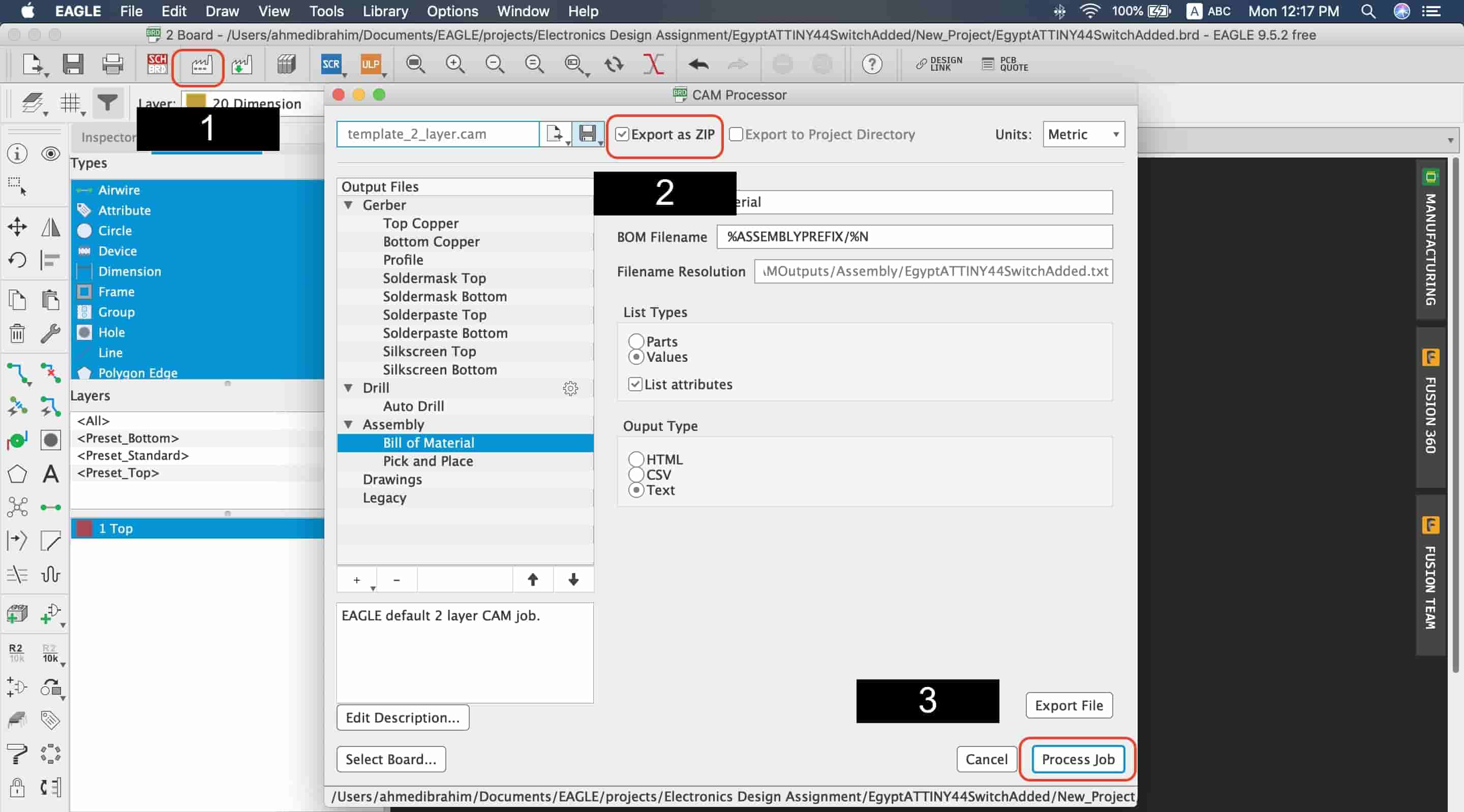
To solve that, we gonna make some extra steps. We need to generate the files that we will send to the machine to fabricate our PCB. First, we need to export a PCB Gerber file.
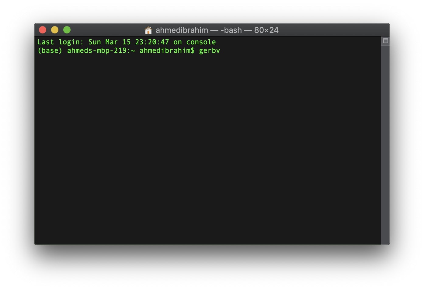
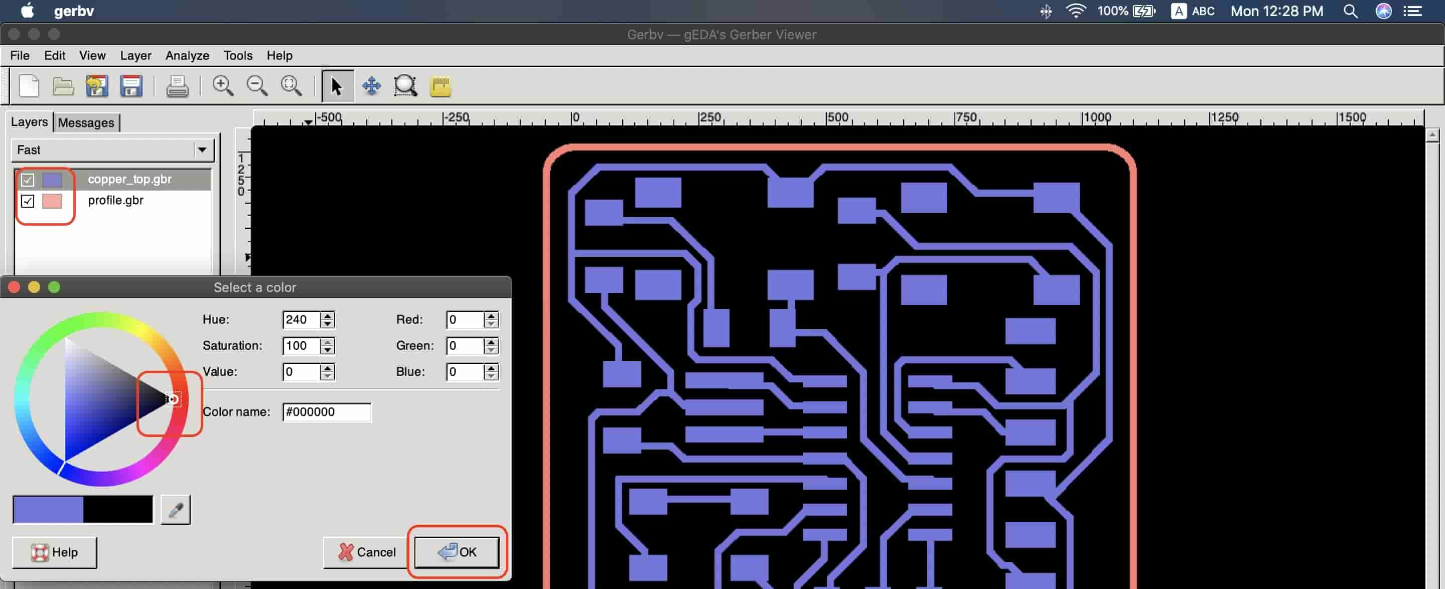
After that, we will open that Gerber file using the “gerbv” program. For more information on how to install “gerbv” see this link. Installing It is very simple. Launch “gerbv” by typing gerbv in the terminal.
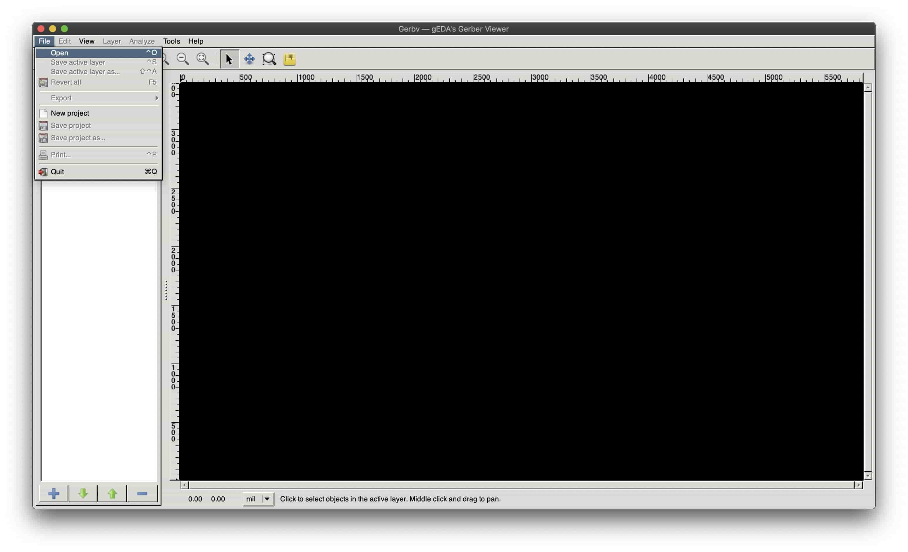
Open the Top copper and the dimension layers on gerbv, Then make the color of both layers black.
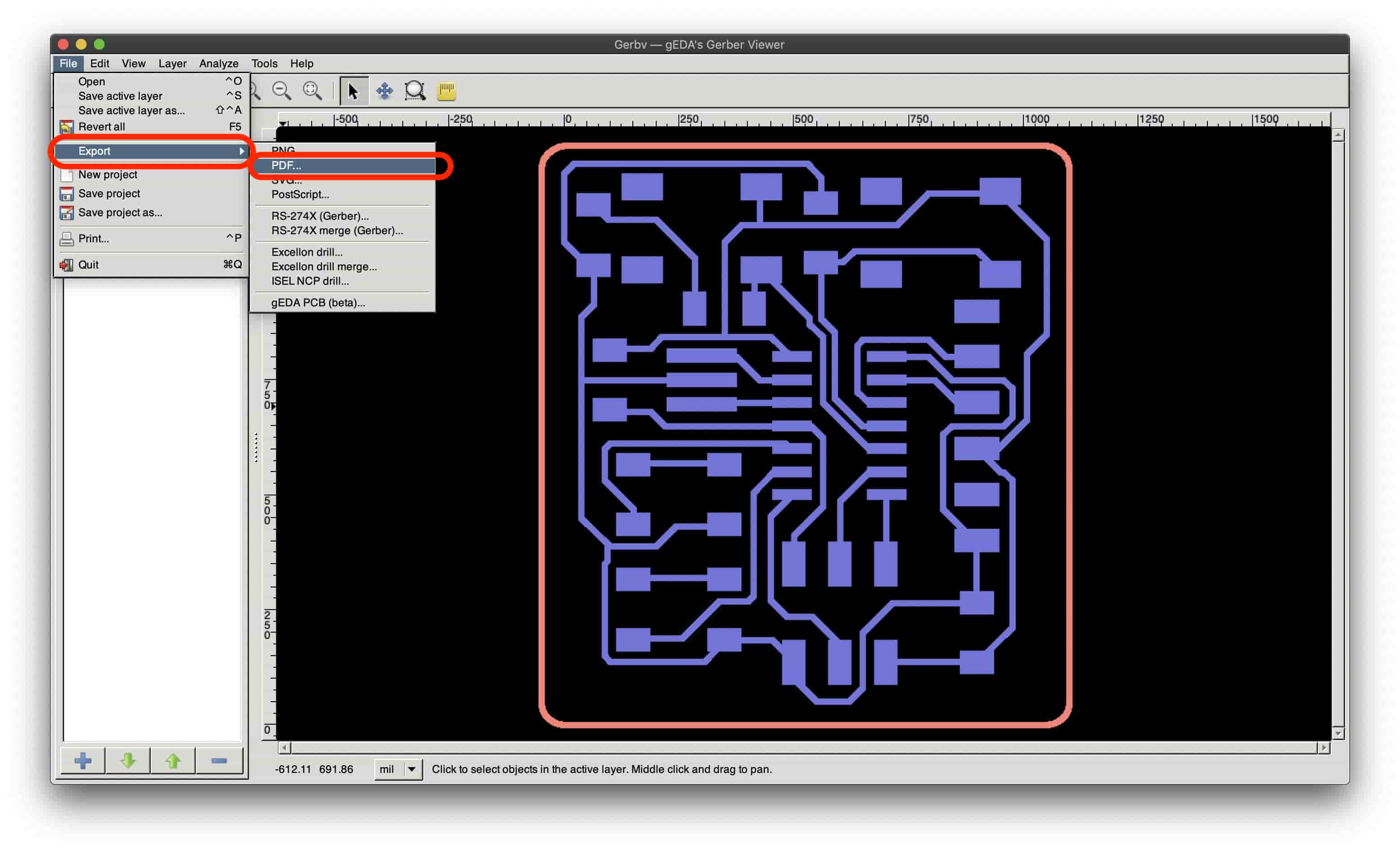
We need to export these two layers as one PDF file.
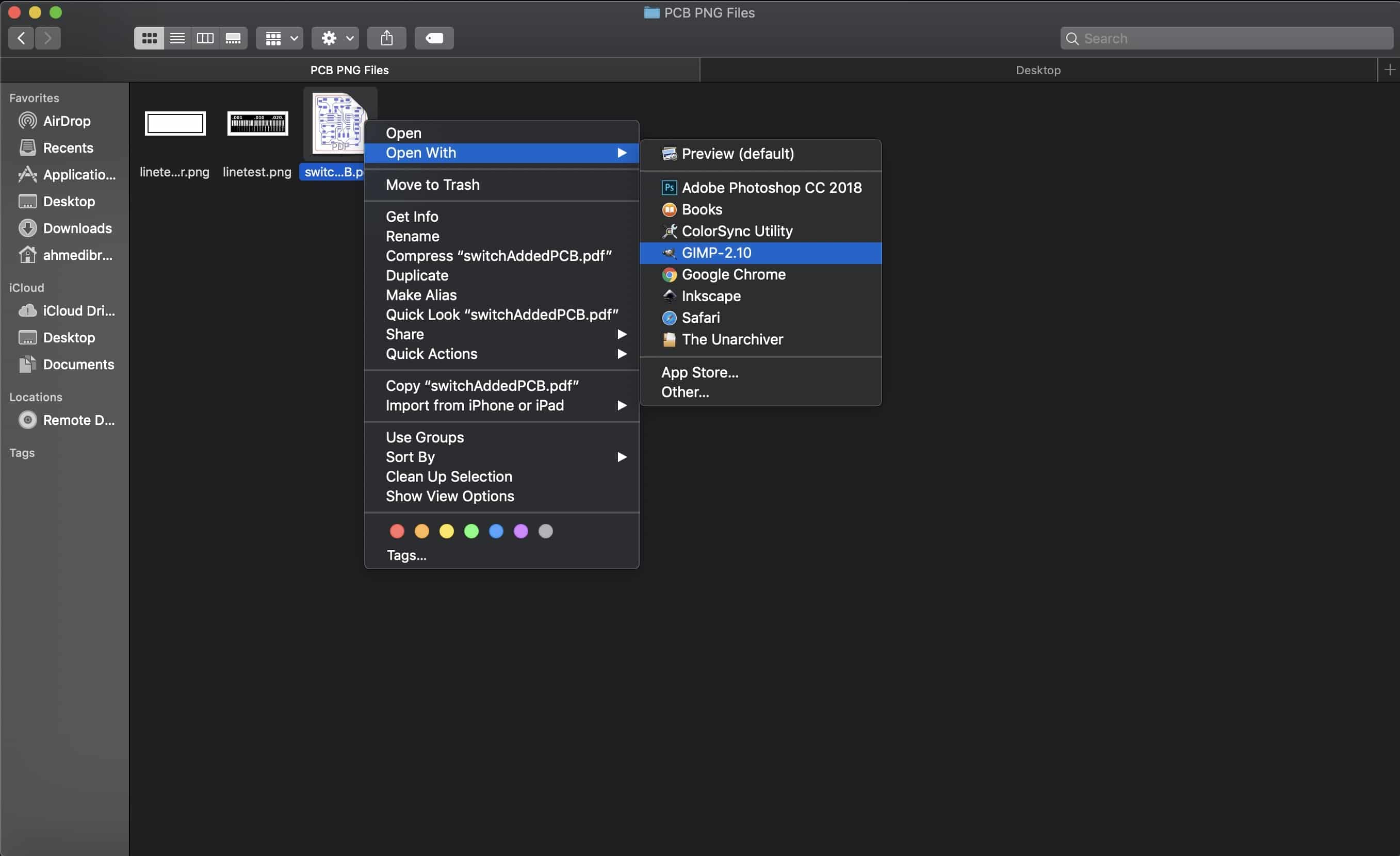
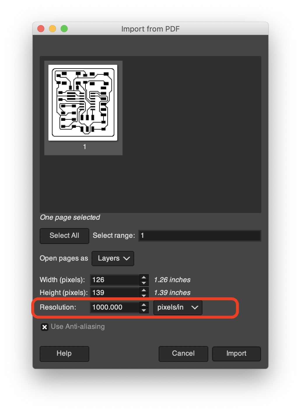
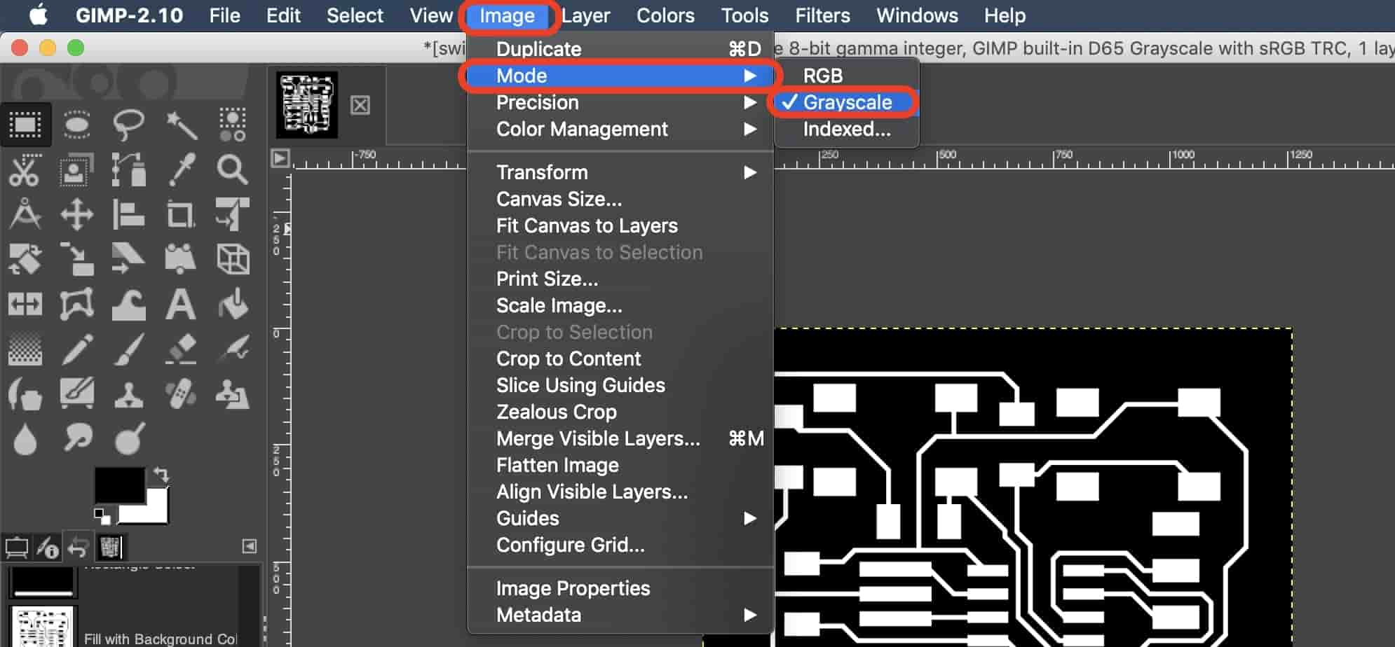
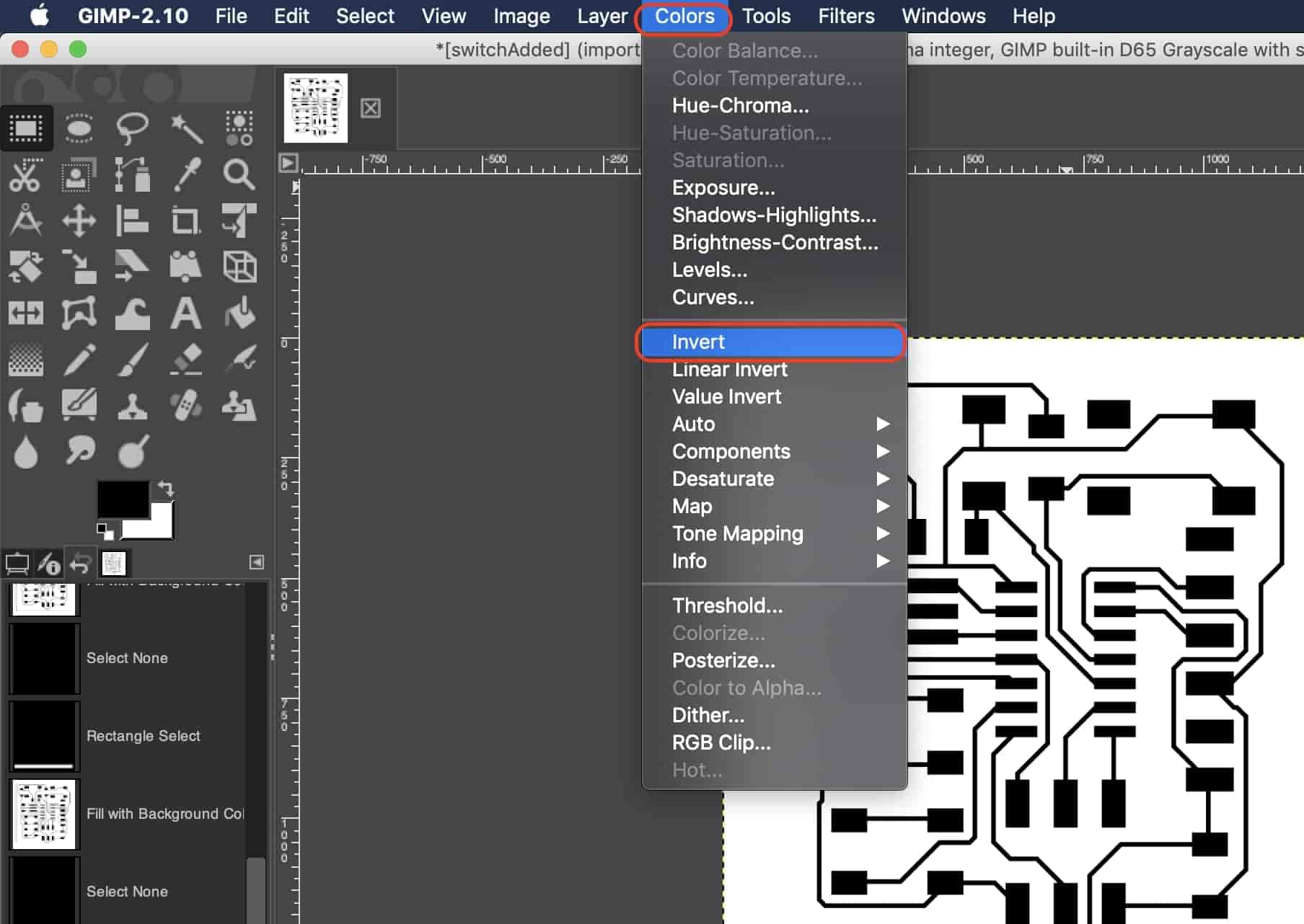
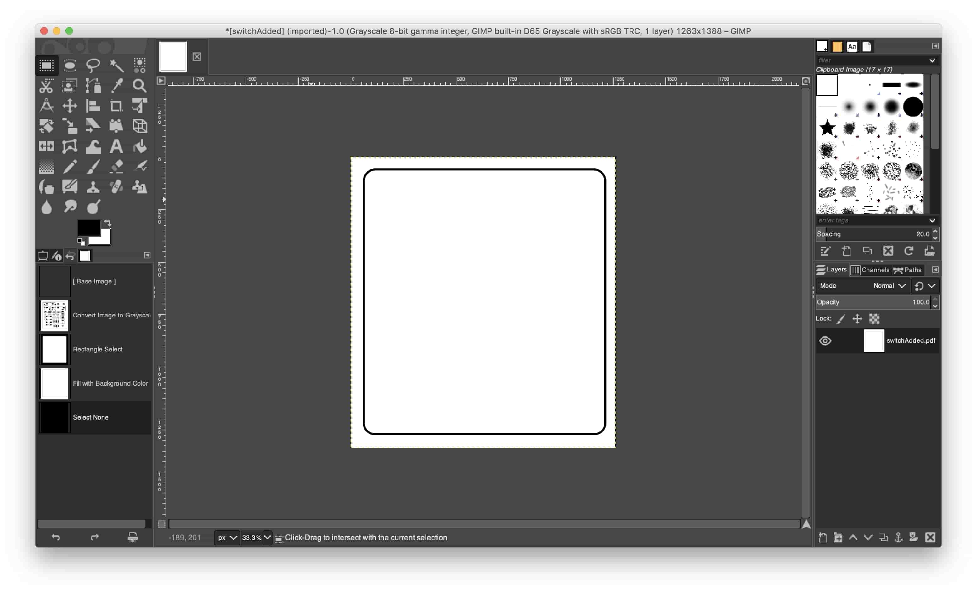
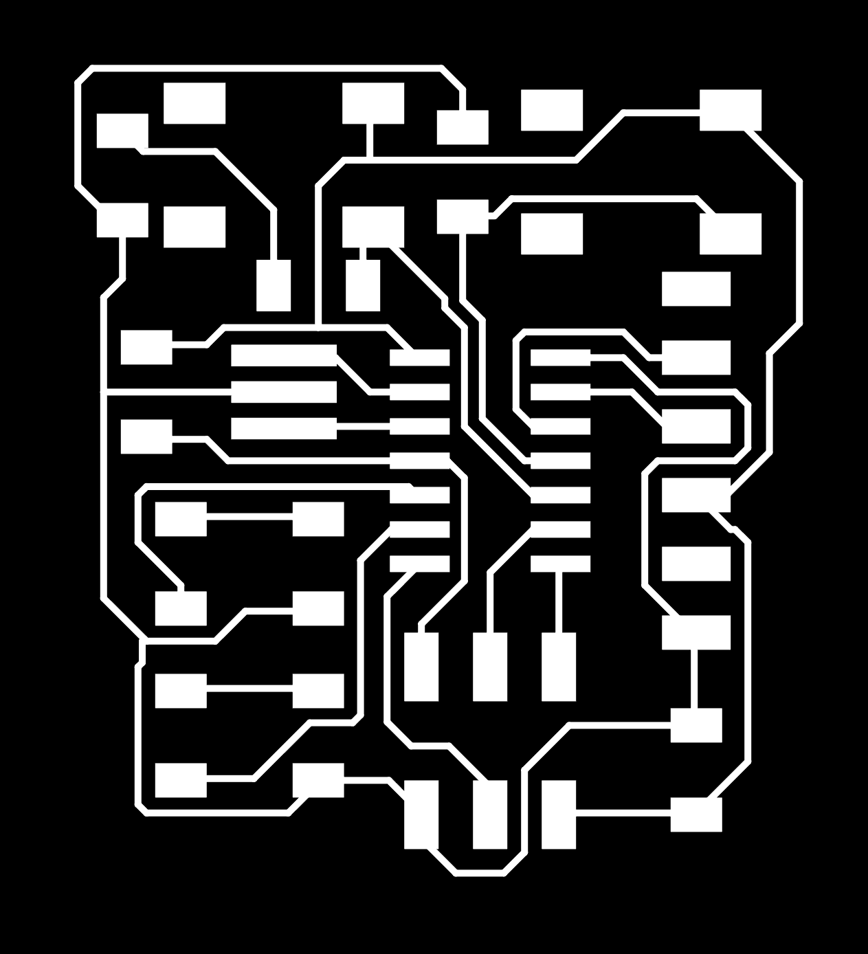
We need two images for the PCB to be millied one for traces ( traces white and background in black) and one for outline(outline in black and background in white). We gonna do that process on GIMP its a free open-source photo editing software. Open the PDF file on GIMP with 1000 DPI resolution, then changed the color mode to “Greyscale”
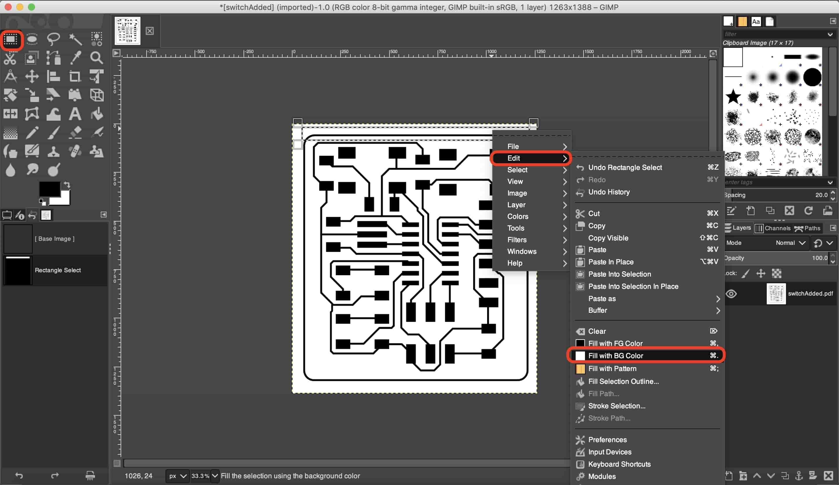
Then using the selection tool, I selected all the four outerlines and fill them with white color.
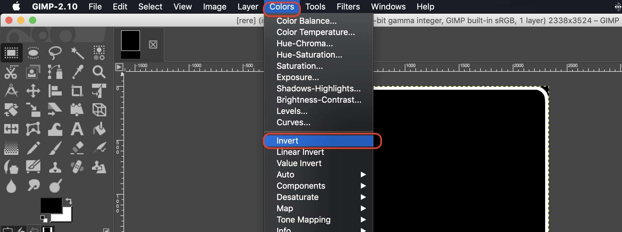
And I repeated that with the remaining three outerlines, now I shhould have only the traces for my PCB. Then I inverted the colors from colors -> Invert.
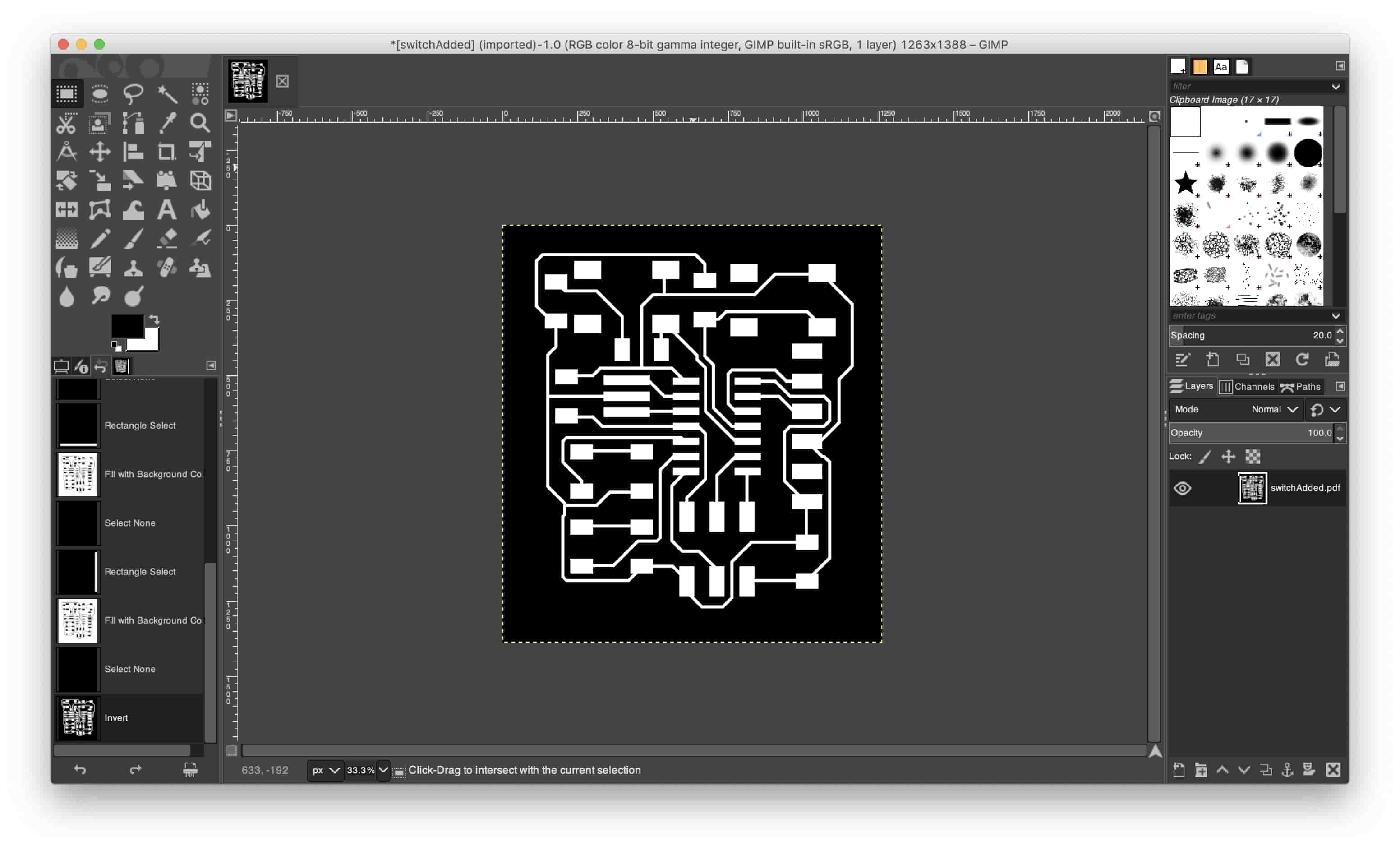
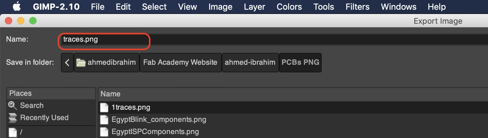
Now, I need to export the traces only as a PNG file.
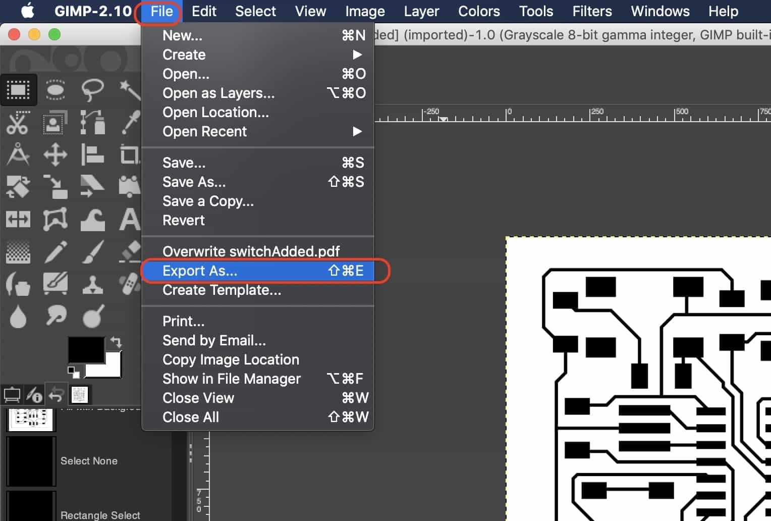
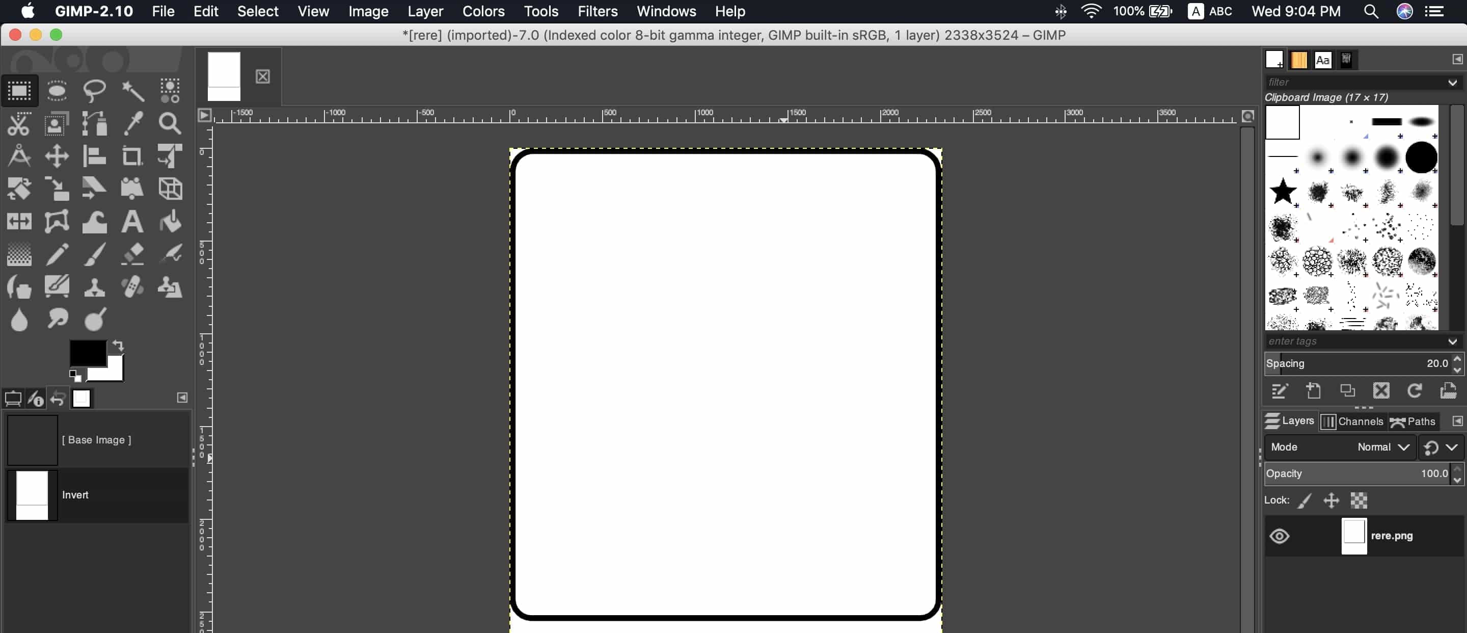
After exporting the traces PNG, I will repeat the previous process but with the profile image, I will UNDO all the things that I changed inthe PDF file, then delete all the traces and leave only the outerlines, then export the PCB board profile only as a PNG file.
Now we should have two PNG files, one for the traces and one for the PCB profile.

Exporting Fabrication files(WINDOWS USERS).
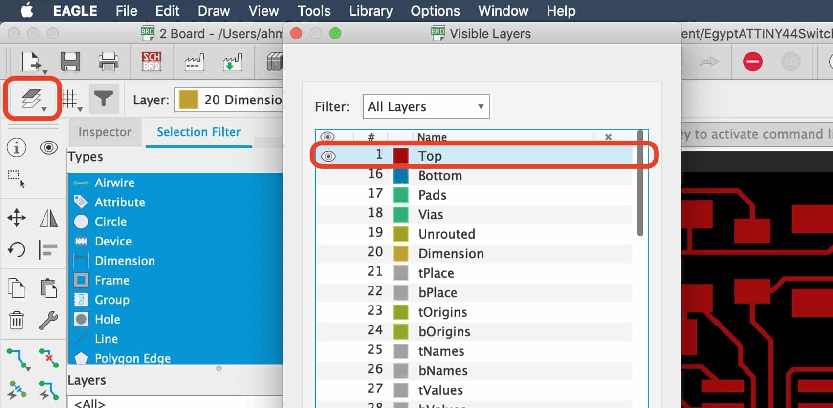
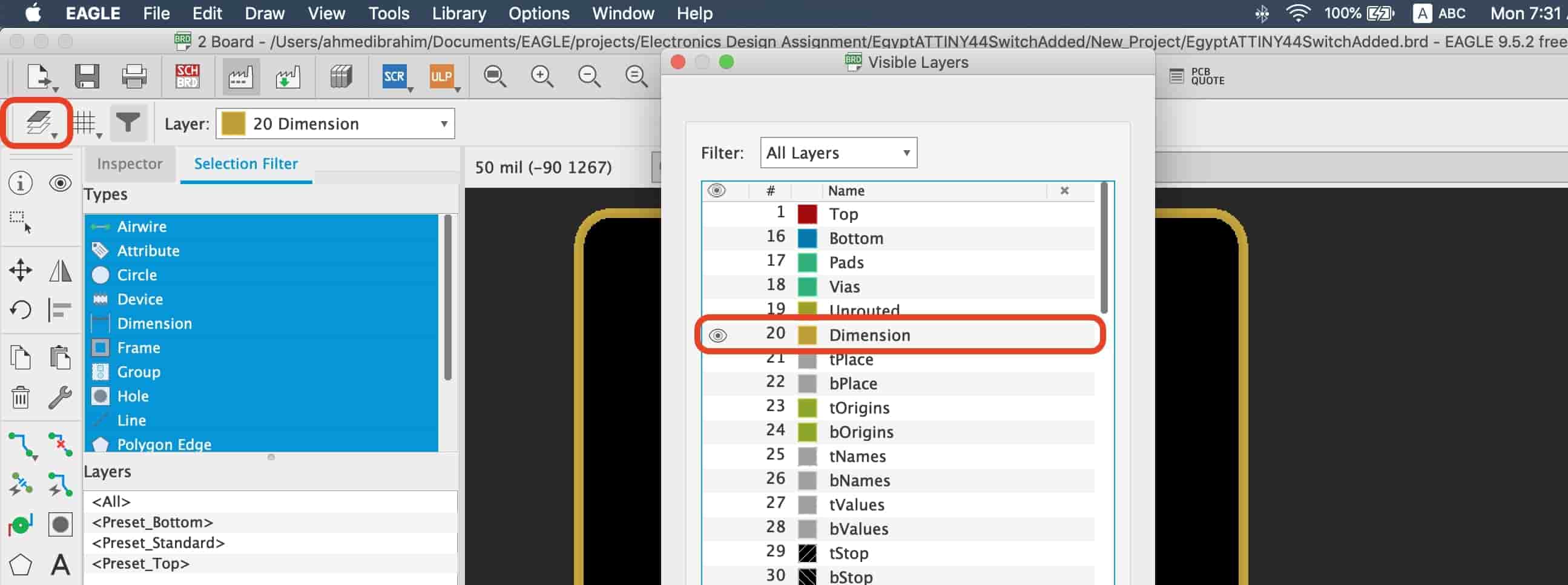
In the PCB board layout file, we gonna hide all the PCB layers except the top layer.
Then export that image as a monochrome image at 1000 DPI resolution.
We gonna repeat that process again but with the PCB profile, hide all the layers except the dimension layer. Then export the PNG image with the same previous settings.
But we need the outline in black and background in white, so we have to open GIMP to invert the colors.
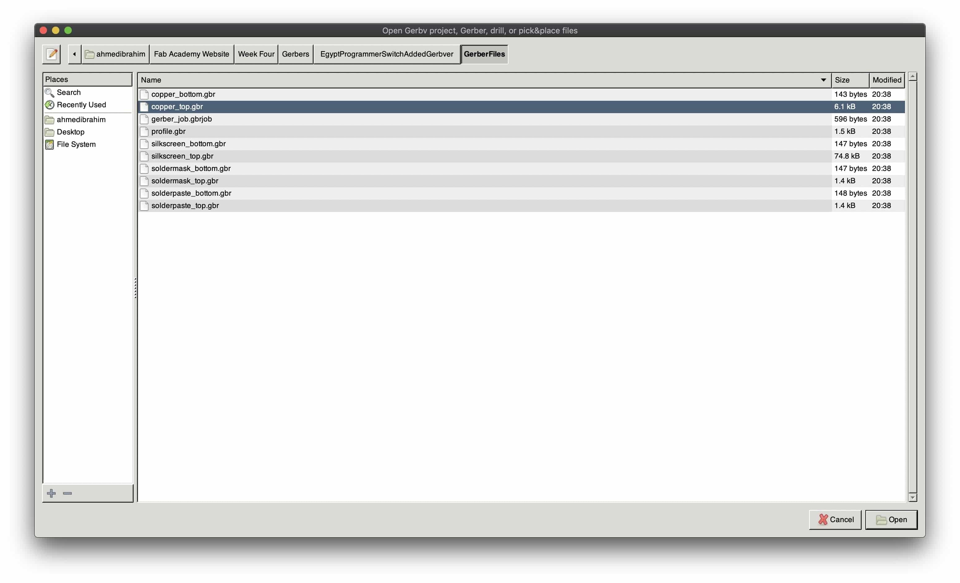
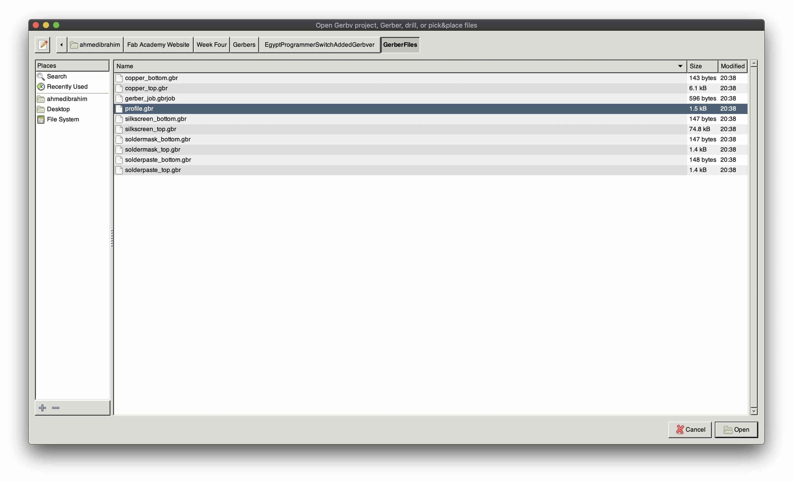
PCB PNG Files Download
Fabrication Process
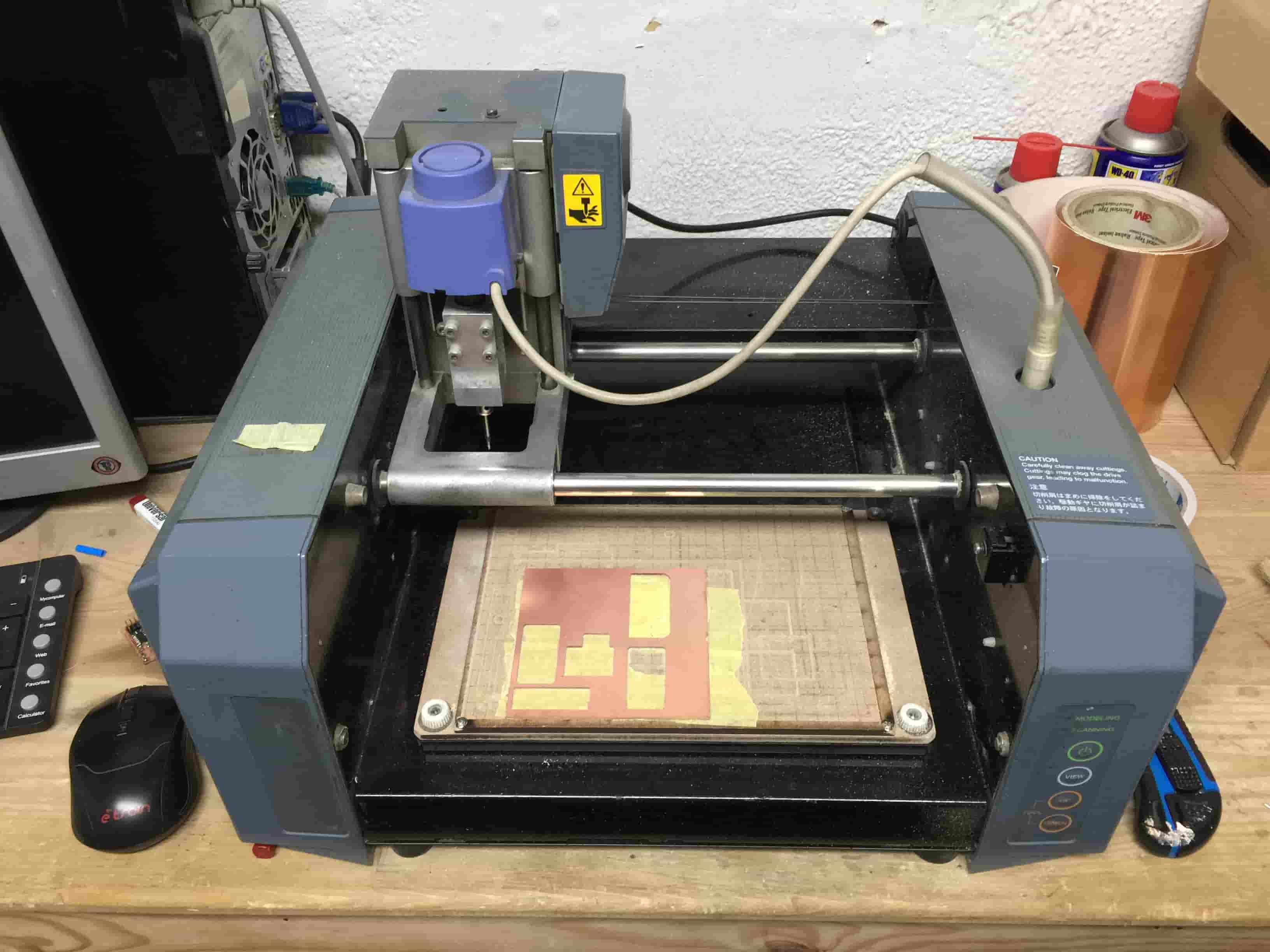
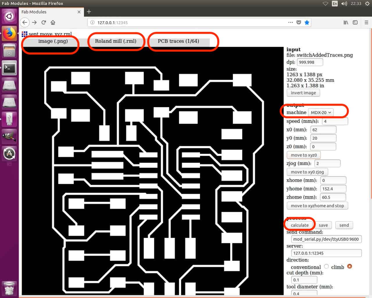
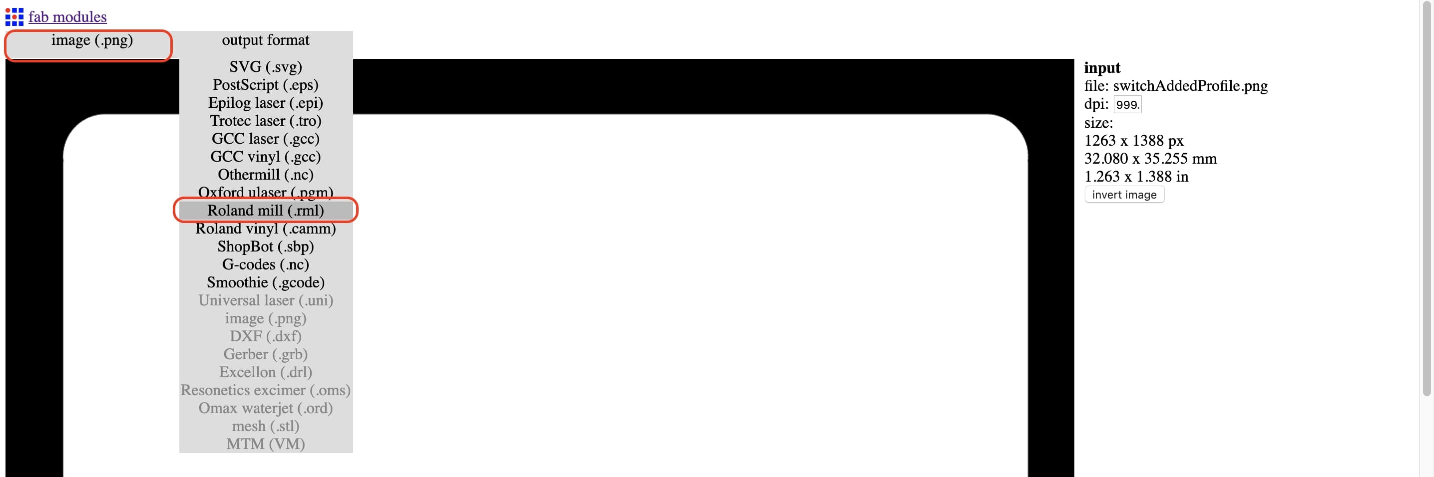
Now we need to open Fabmodules to import our PCB PNG files to it, Fabmodules will process and translate these PNG files to a language that the machine can understand to tell the machine how to fabricate our board. Now we have to import the traces PNG image to Fabmodules and set all the parameters as following.
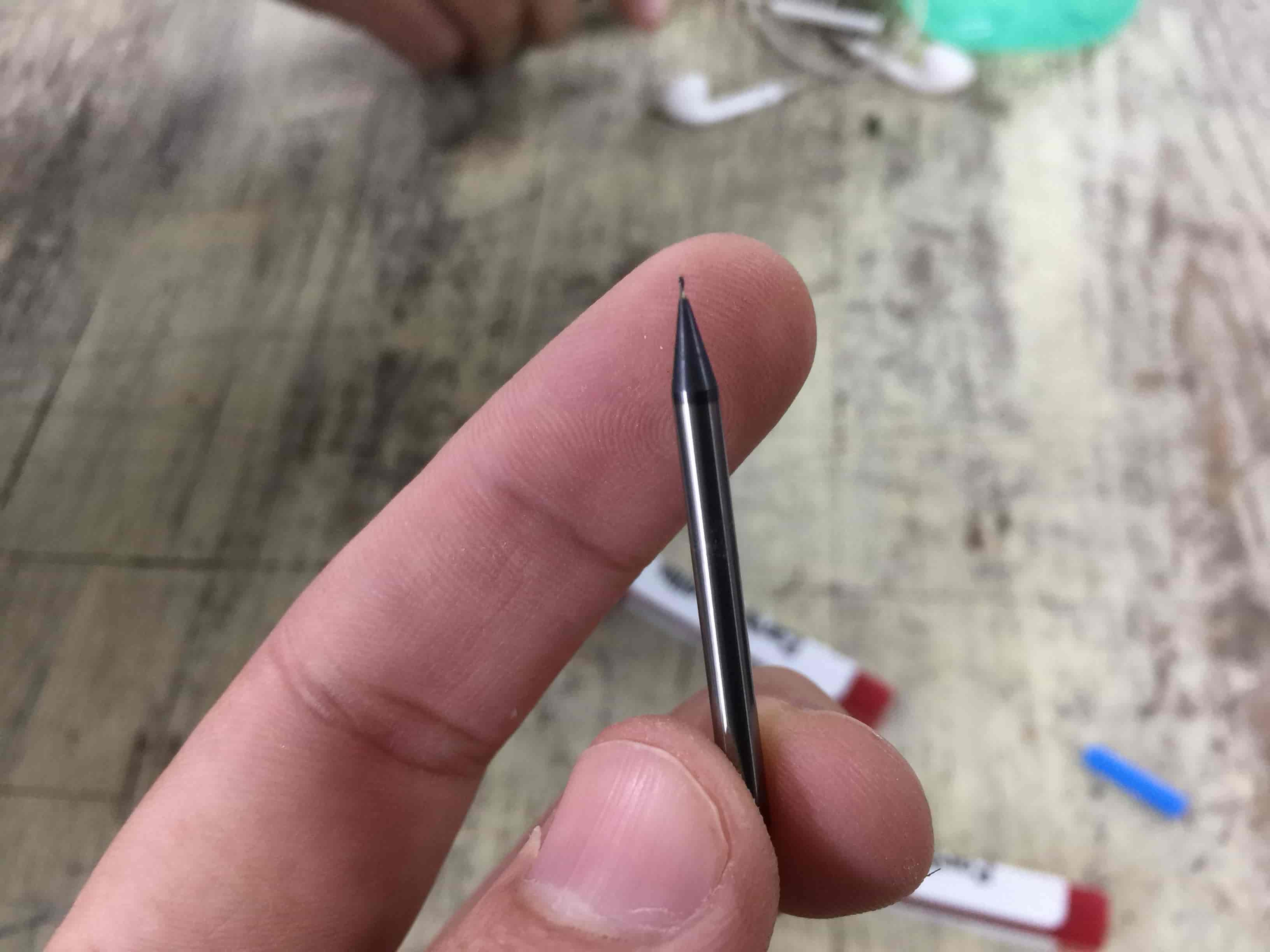
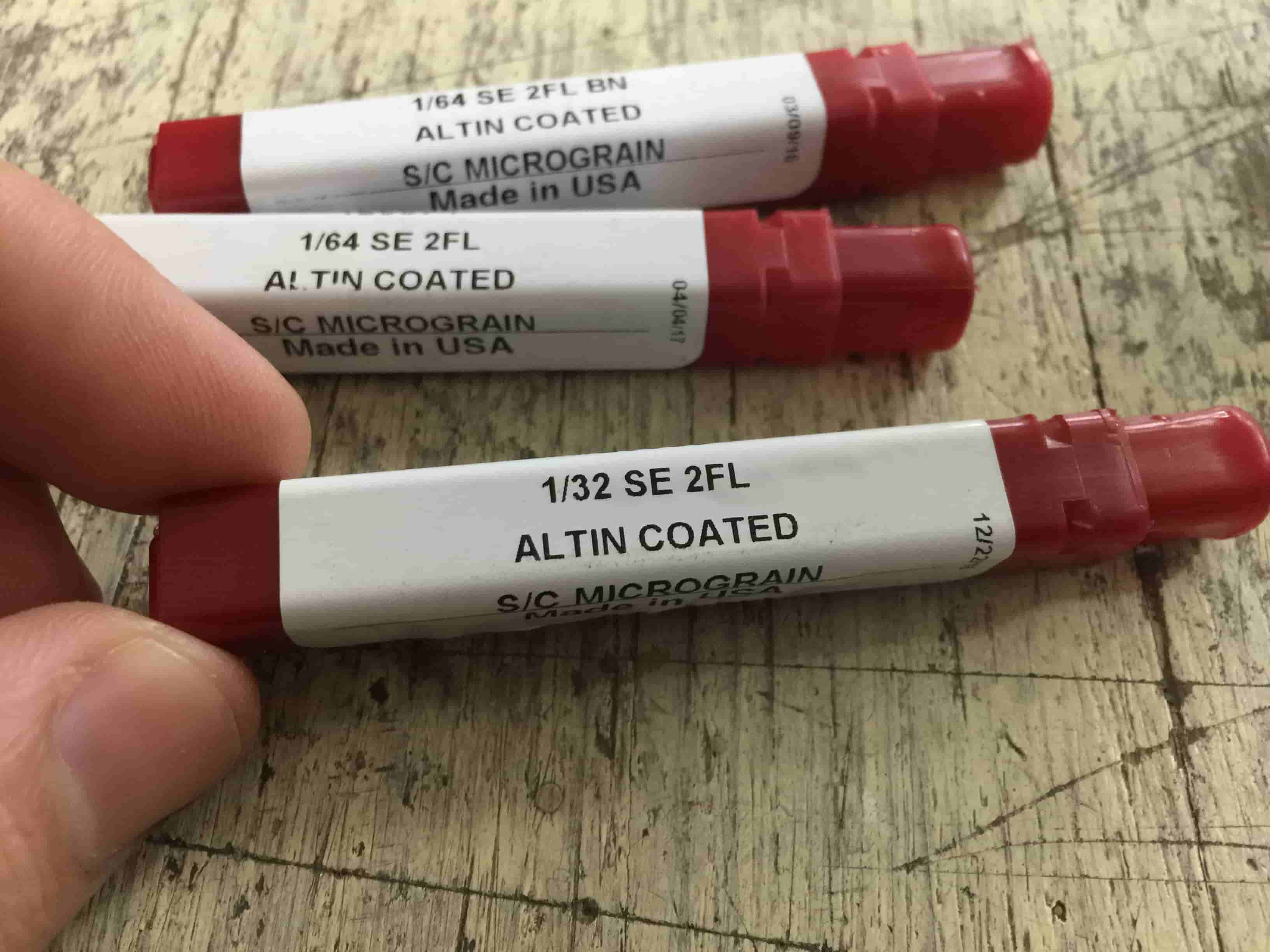
Then press on the “Calculate” button to calculate the toolpath, we need to check carefully if the toolpath is passing correctly between all our traces without problems or not. After making sure that everything is alright. And after installing the right endmill in the machine(1/64 inch) and setting the machine origin, press the “send” button to send our job to the machine.
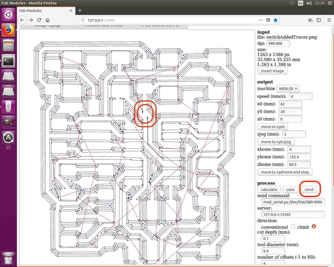
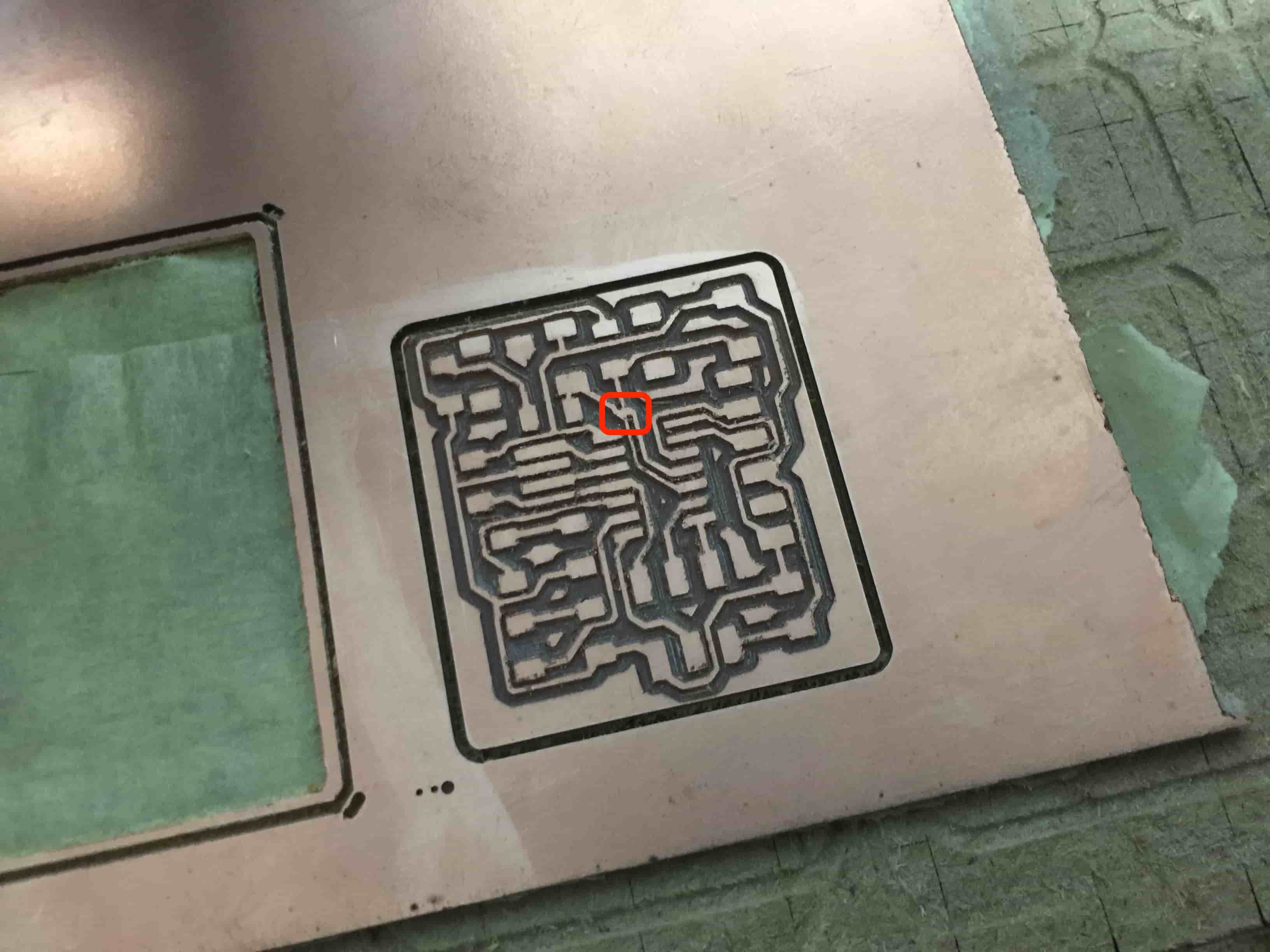
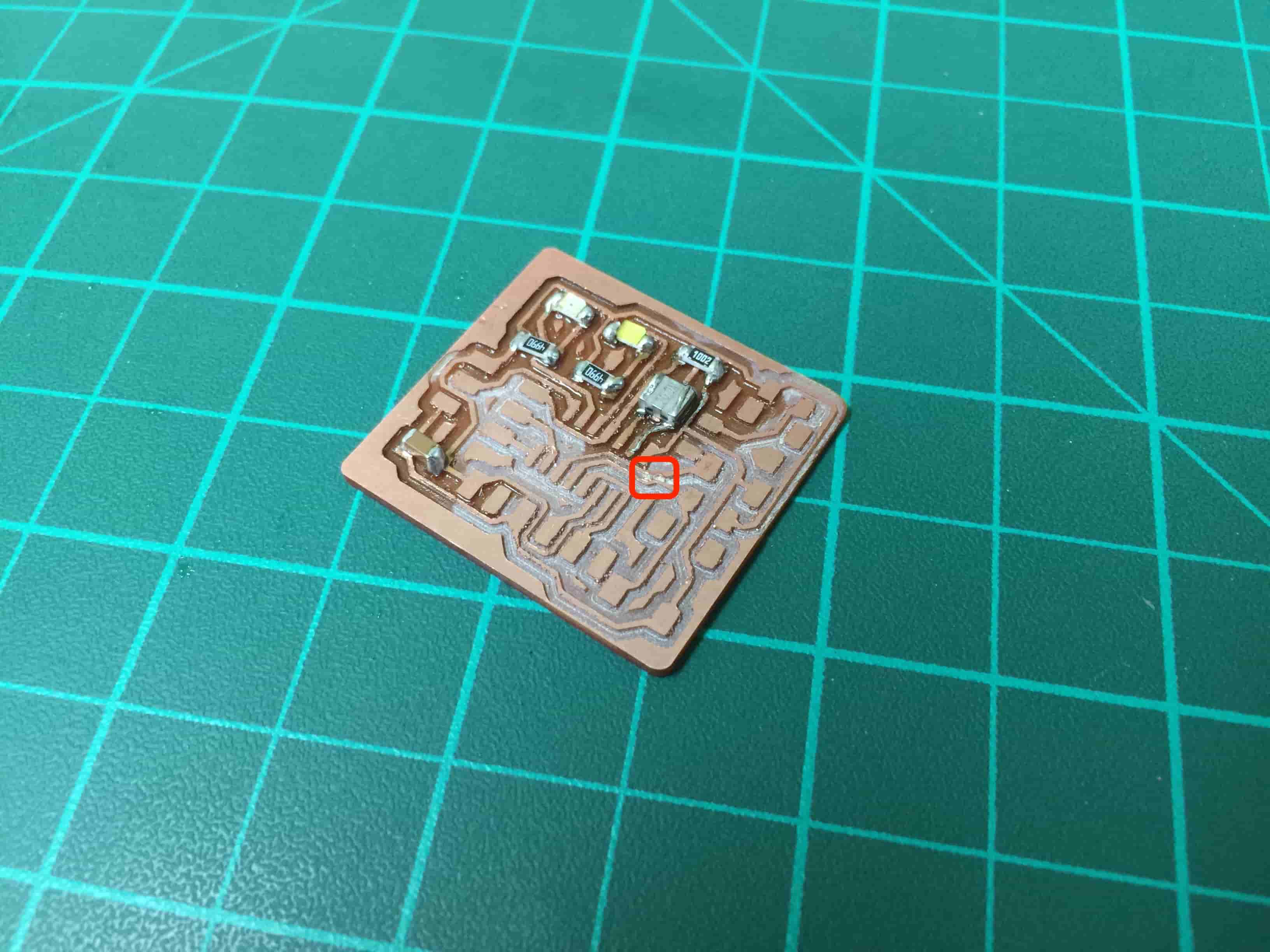
As you can see in the third image, there's a short circuit between two traces. Actually, I didn't notice it until I finished fabrication the board. I will talk about how did I fix that later.
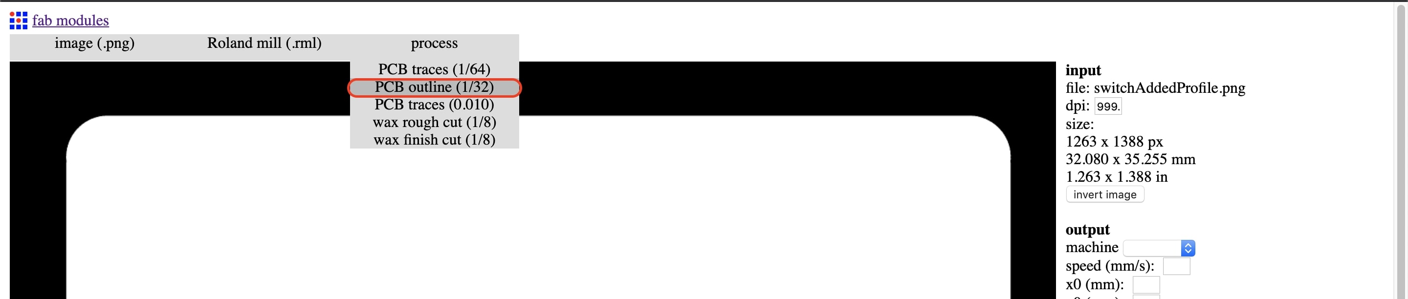
After finishing the PCB traces, we need to import the second image(Profile Image) to Fabmodules, We gonna repeat the same previous process again but with different parameters this time.
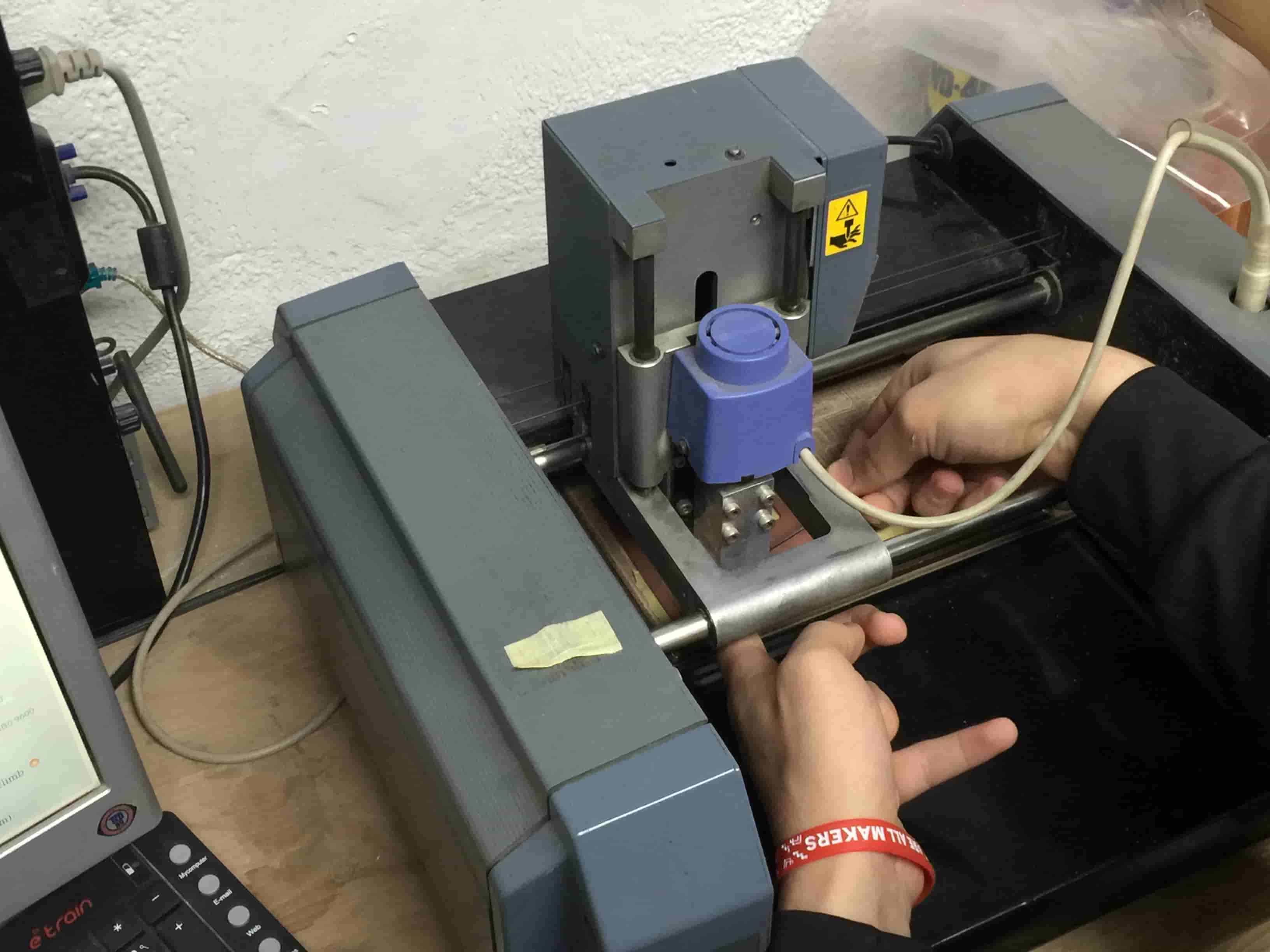
We gonna set the parameters as the previous steps. But, we will change the tool size from (1/64) to (1/32).
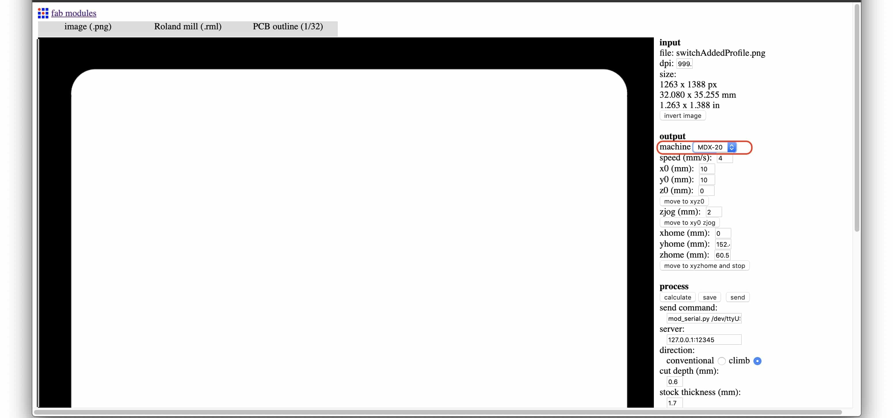
Then we need to change the endmill that we used before to make the traces(1/64 inch) to the bigger one(1/32 inch). Then press the “Send” button to let the machine start its work.
After the machine finished its job, let’s see our masterpiece :D
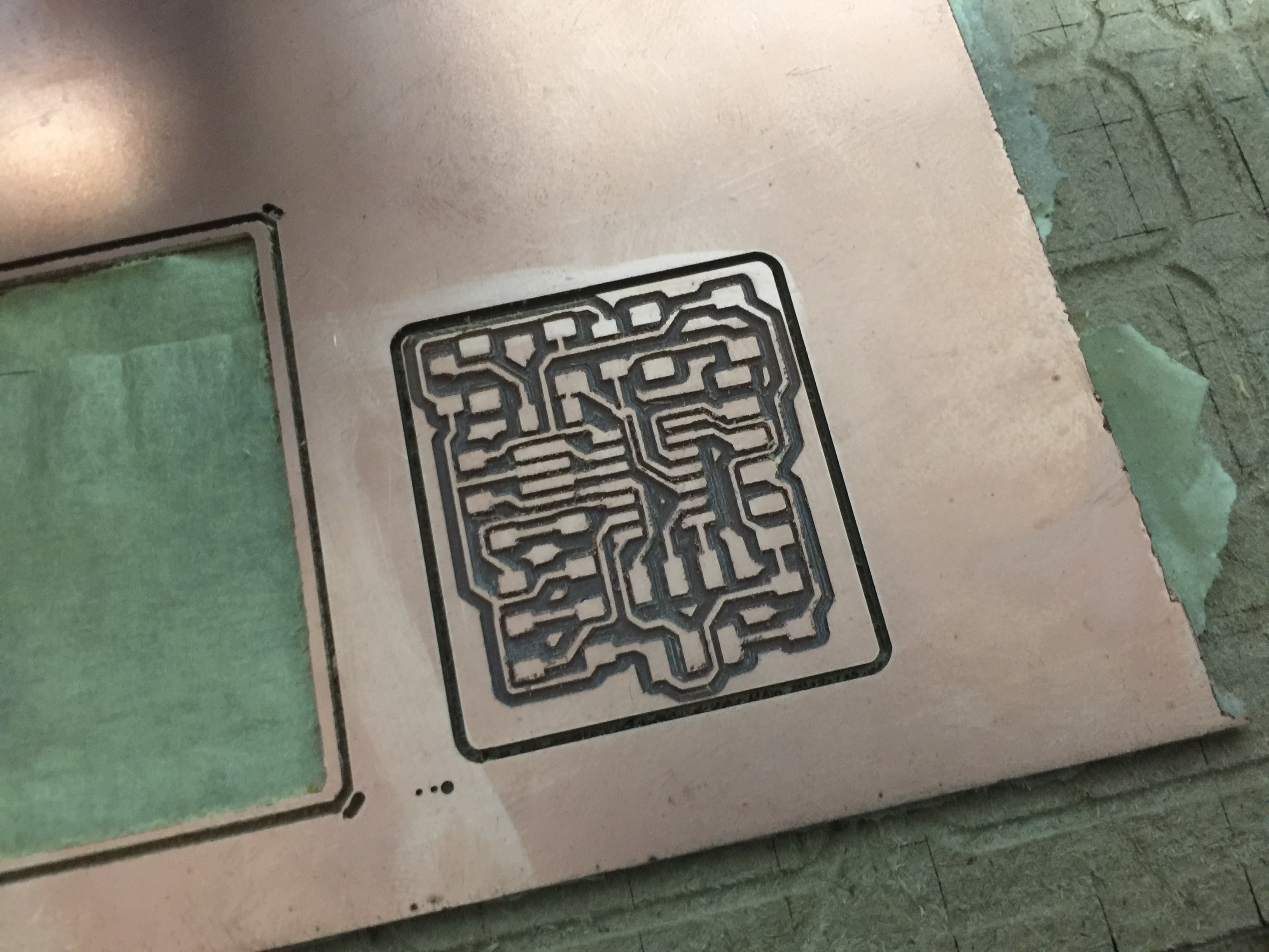
I noticed a small problem, there’s a short circuit between these two tracks. But we can fix that later by separating them with a cutter or something.
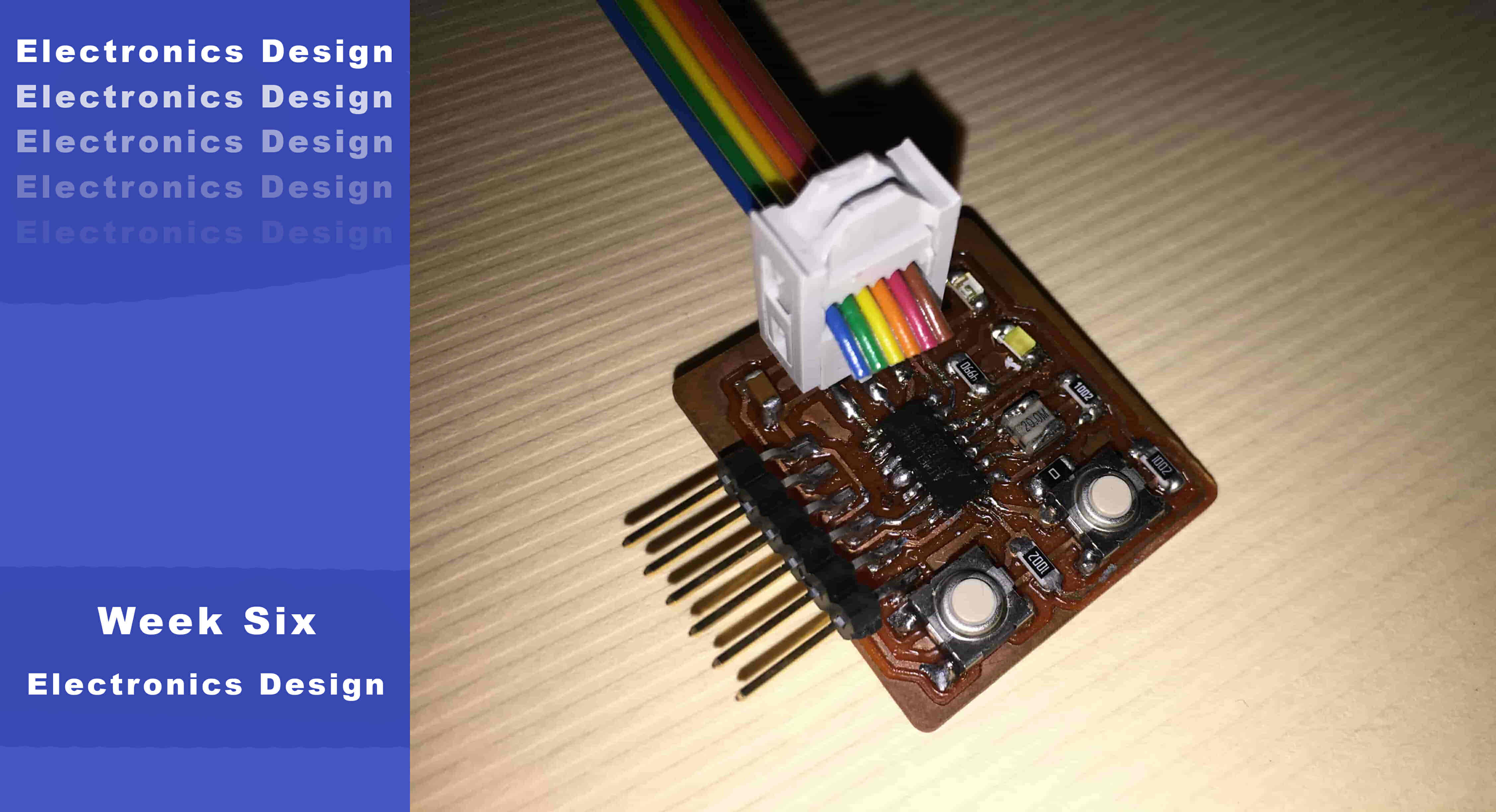
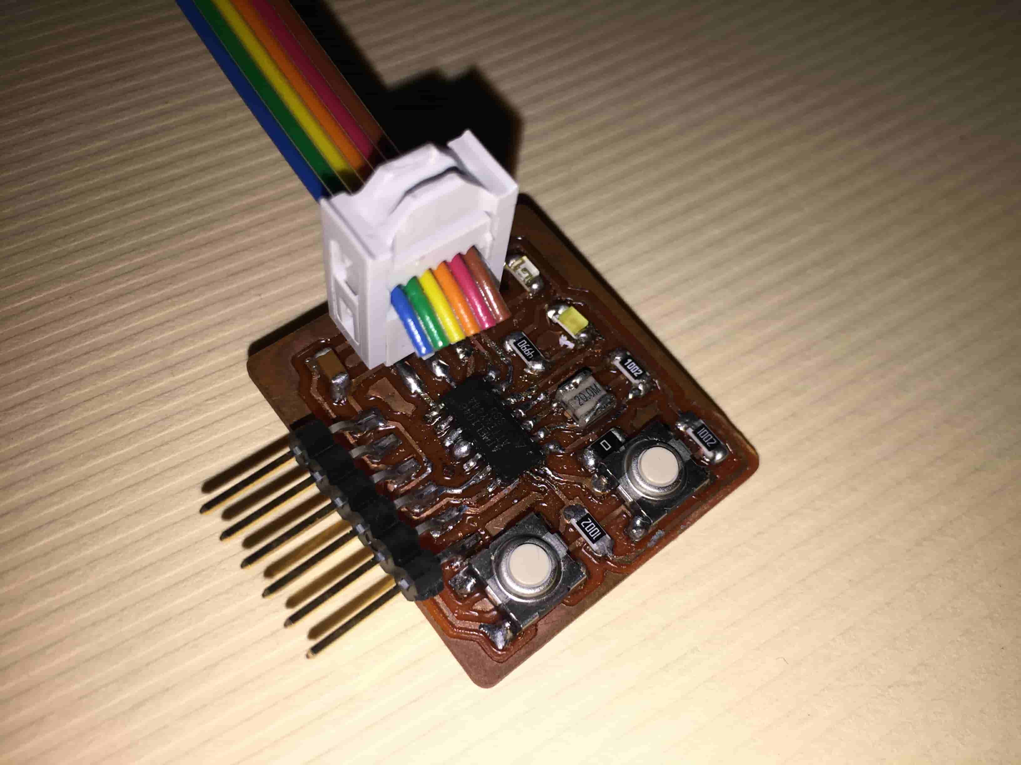
Soldering the PCB
Now it’s the time to solder our hardware on the PCB, preparing the soldering setup and the needed components.
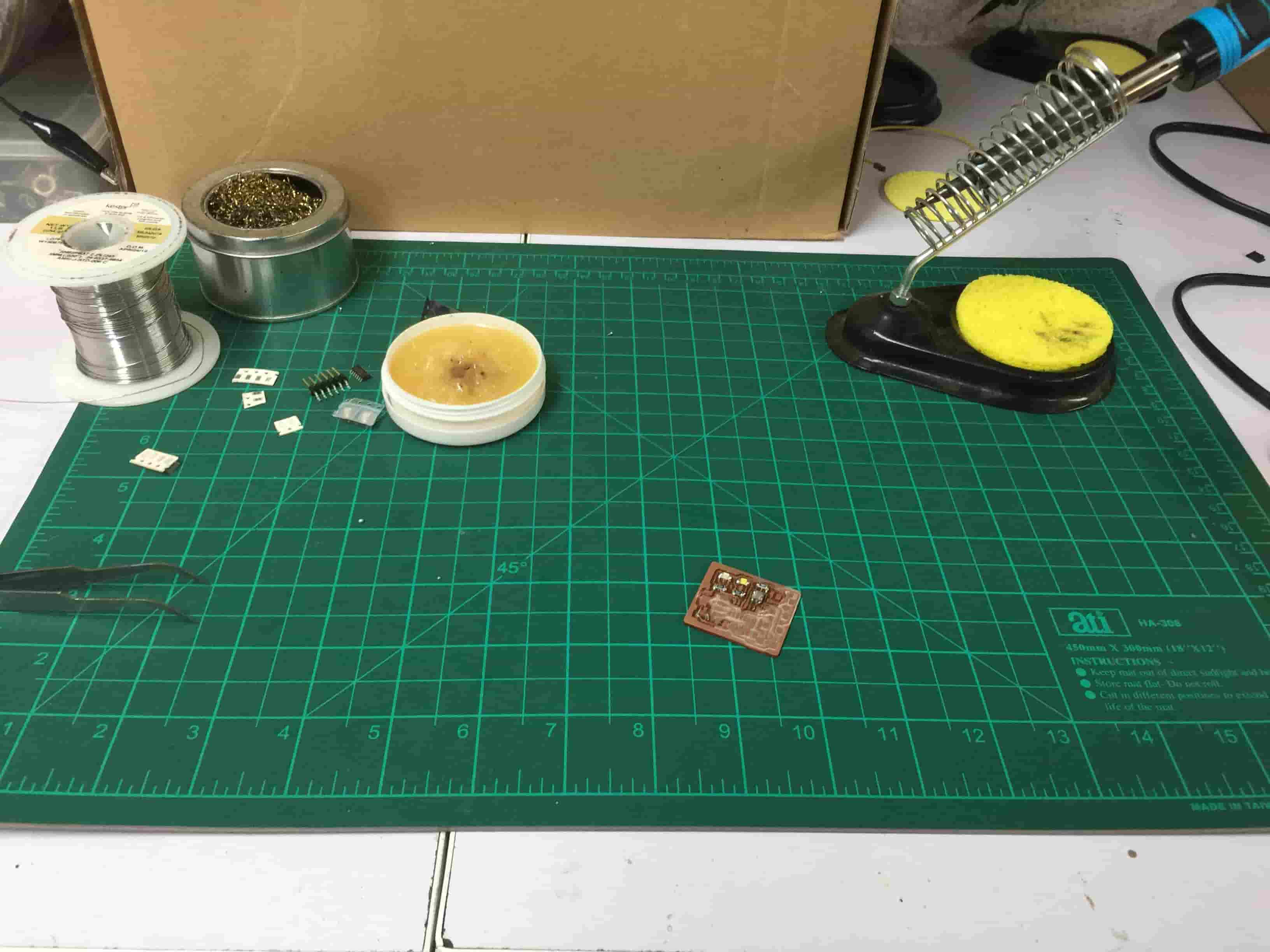
Before I start soldering the Attiny44 chip I fixed the short circuit using a cutter.
Then I soldered the Attiny chip and the rest of the components
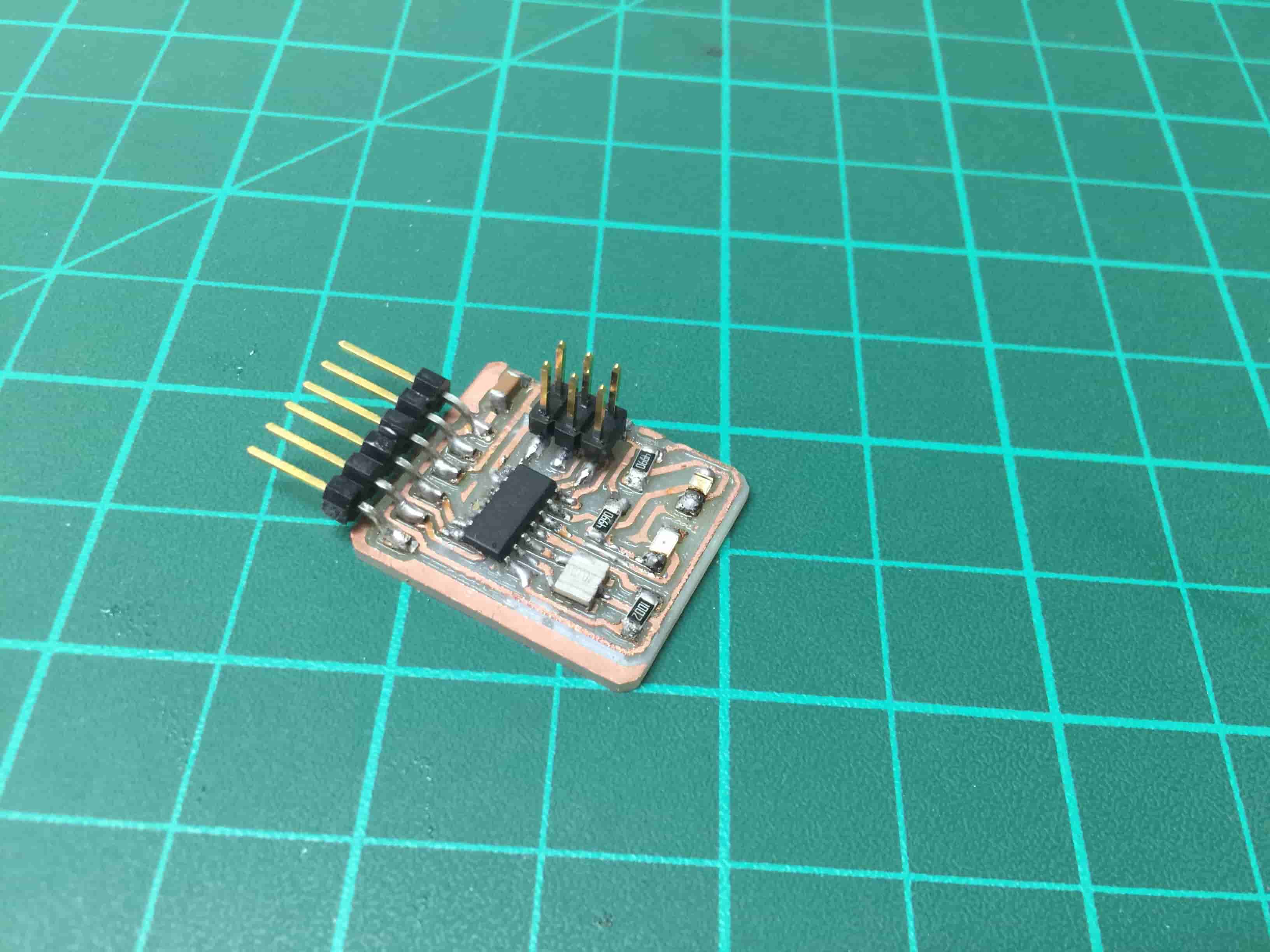
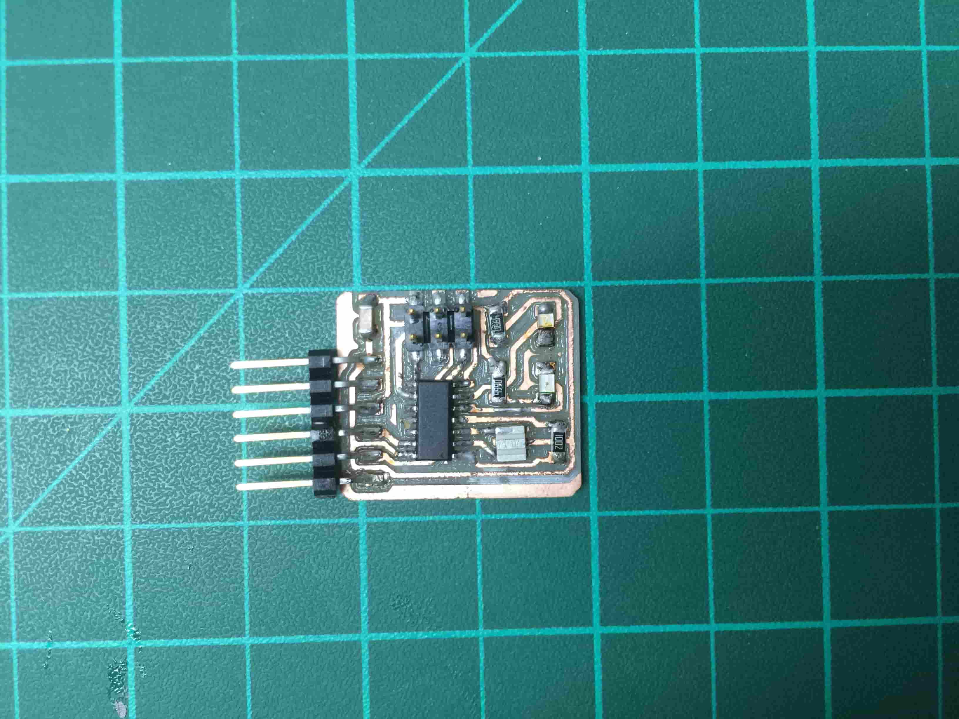
Also, I soldered another board that I designed before.
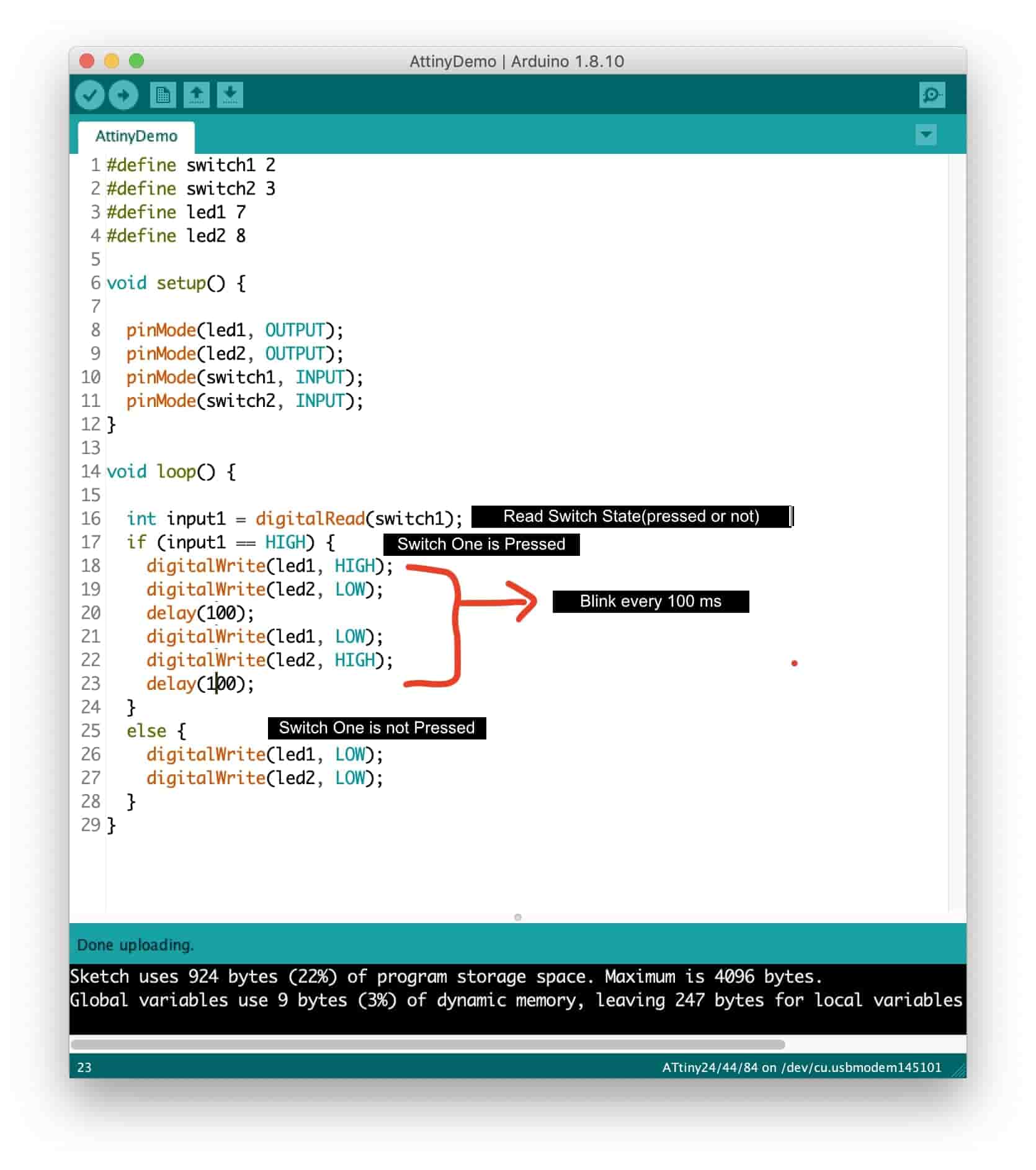
Test Our PCB (BONUS)
I have previous experience with Arduino so I chose Arduino IDE to program my board. Before I start
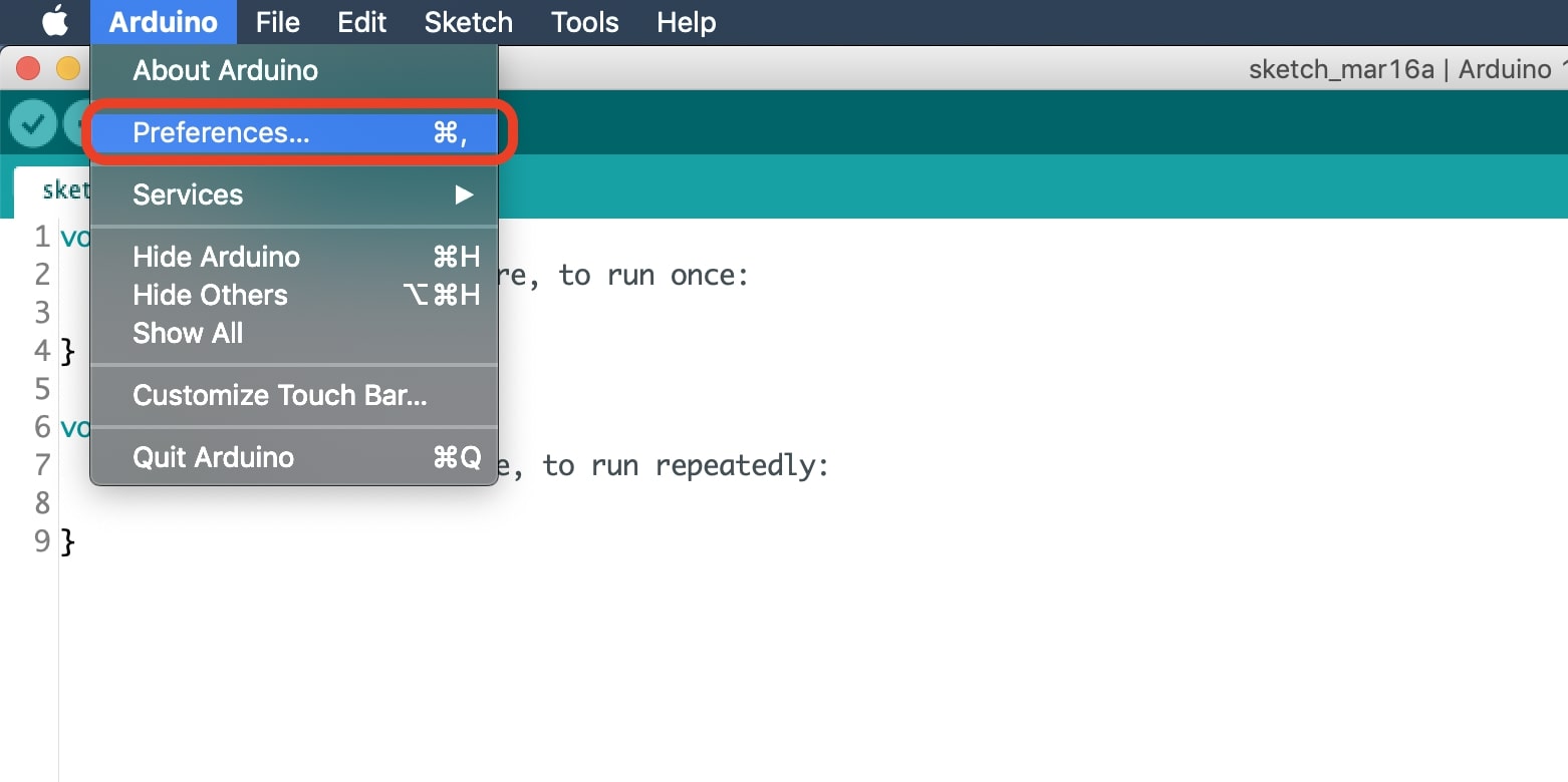
programming, we have to add the attiny44 board to Arduino IDE to recognize it. From the “file” menu
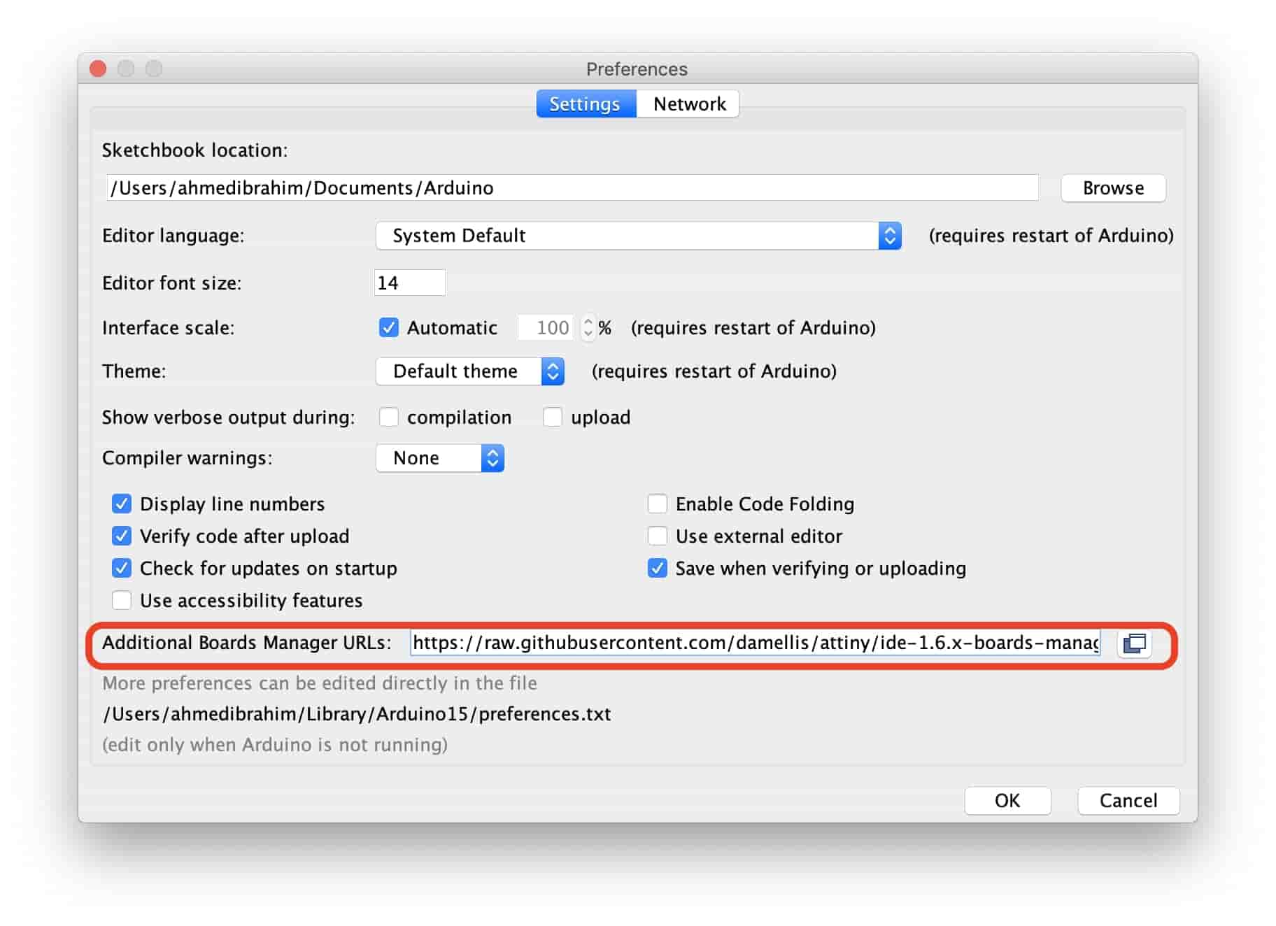
chose “Preferences” Then paste this URL in this place.
https://raw.githubusercontent.com/damellis/attiny/ide-1.6.x-boards-manager/package_damellis_attiny_index.json
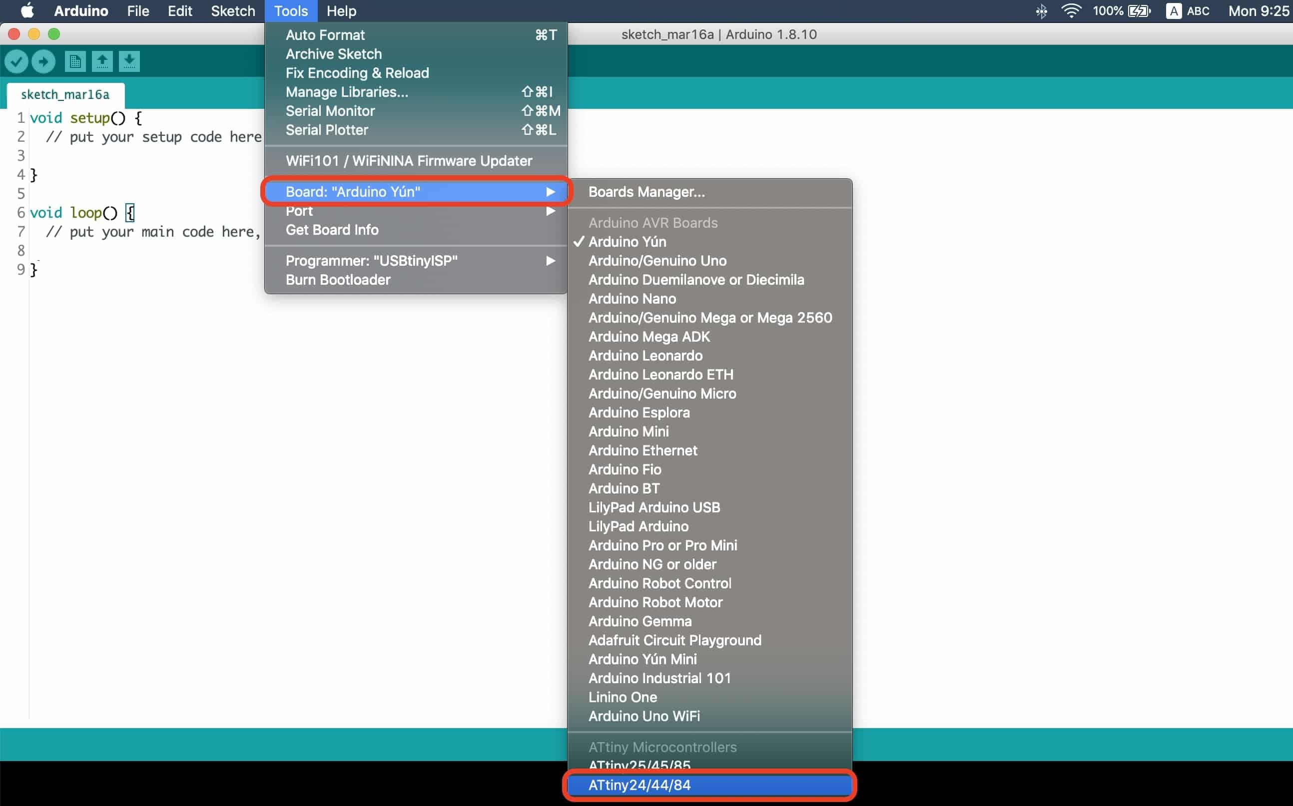
After that, go to the Boards Manager tab
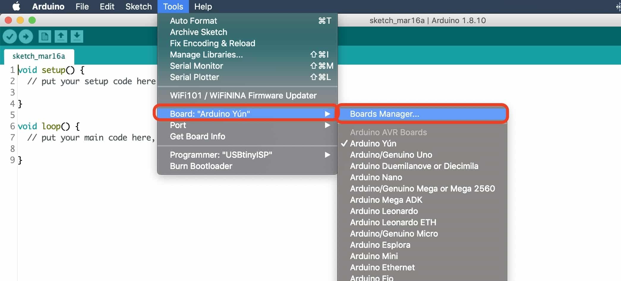
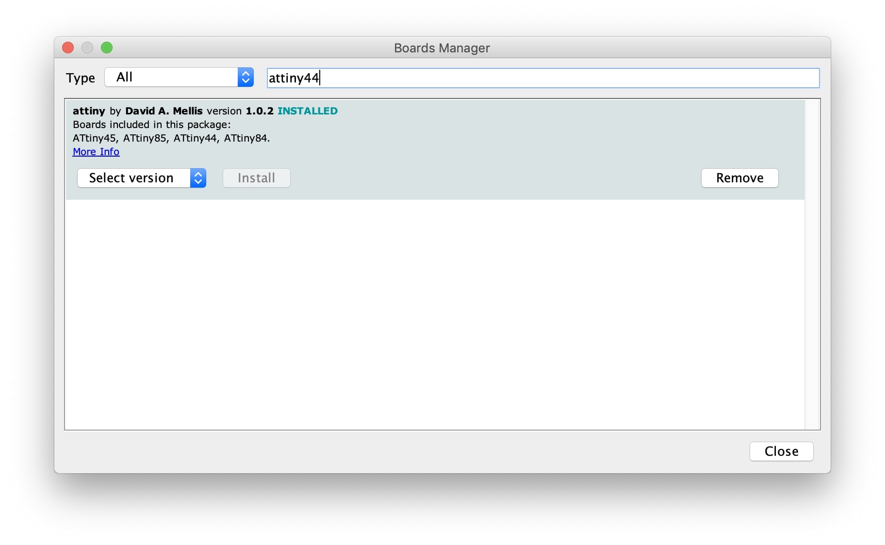
search for “attiny44” and install this library.
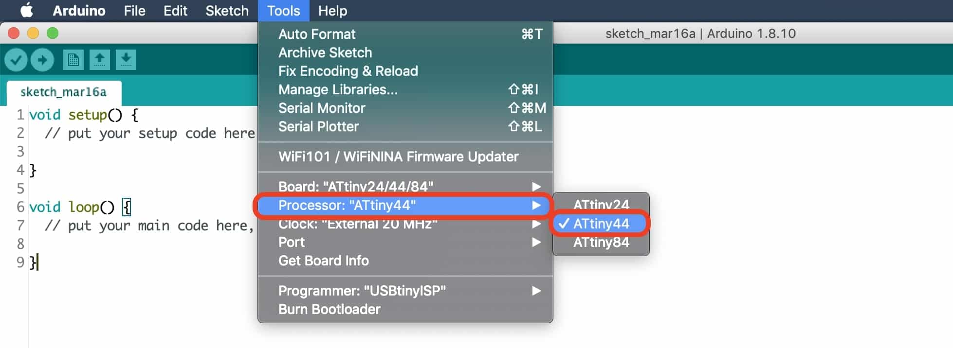
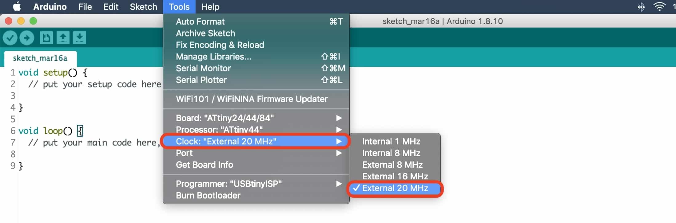
Then, from tools -> Boards we need to choose the chip that we gonna use, in our case its ATtiny44, set the processor to “ATtiny44” and the clock to “External 20MHz”.
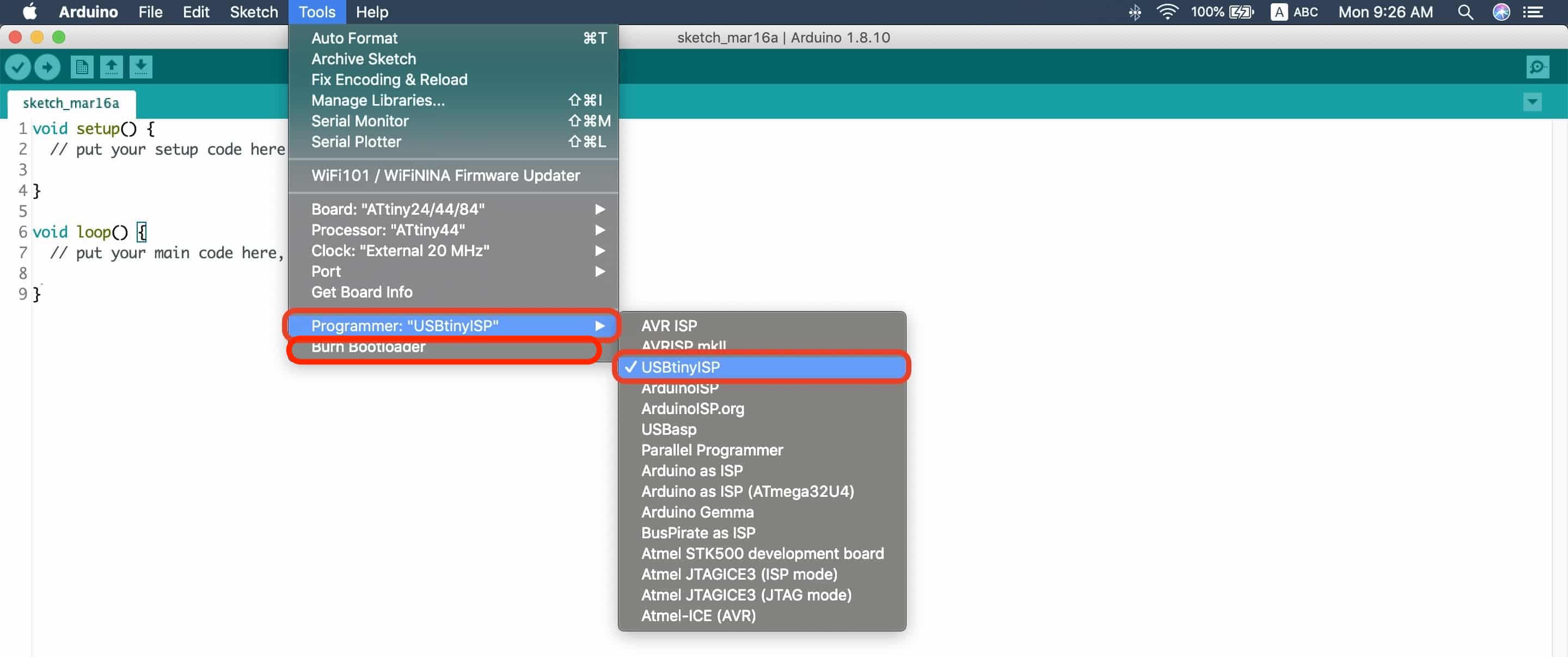
Choose the programmer "USBtinyISP", then upload the Arduino bootloader to the attiny44 chip to set the timer fuses and all of these boring stuff.
Now we are ready to write the code and upload it to our board.
Final Video for the PCB working in action.