Week 04
Electronics Production
01
Assignments
- Group assignment.
- Characterize the design rules for your PCB production process: document feeds, speeds, plunge rate, depth of cut (traces and outline) and tooling.
- Document your work (individually or in group).
- Individual assignments
- Make an in-circuit programmer by milling and stuffing the PCB, test it, then optionally try other PCB fabrication process.
Software
Download File
Resource
02
Assignments
Group Assignments (1)
Characterize the design rules for your PCB production process: document feeds, speeds, plunge rate, depth of cut (traces and outline) and tooling.
Document your work (individually or in group)
The assignment consists of describing the equipment, processes and workflow both in the handling and use of the machine and in the testing area, allowing us to be necessary to take the relevant corrective measures. In this case we will use the model that measures:
- Size of the machine: (330 mm x 400 mm x 310 mm).
- The work area or bed is (180 mm x 300 mm) or 54,000 mm2.
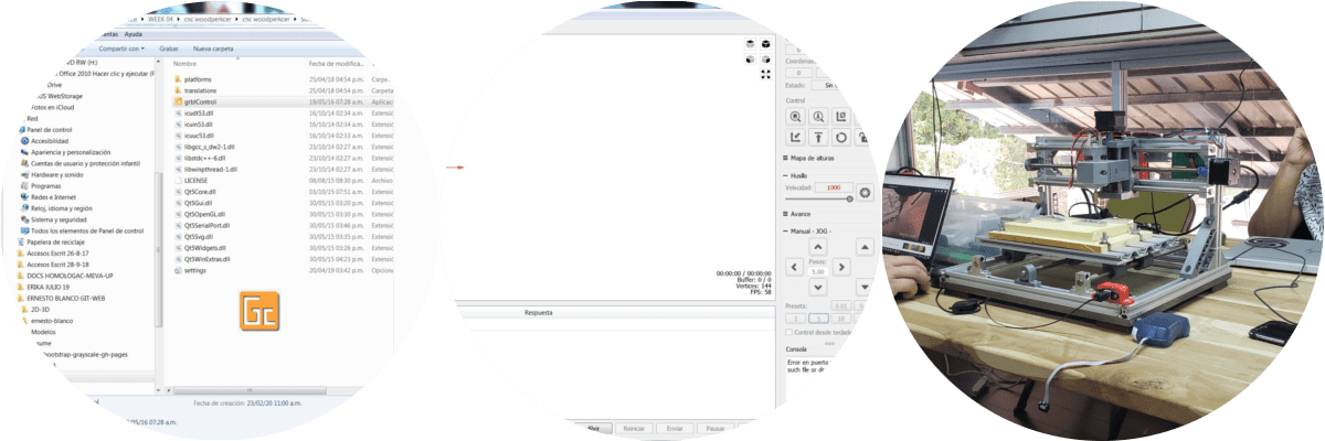
Download the folder with the drivers of the machine to prepare the PCBs from the tutor's Dropbox, since this is auto-executing without installation on the laptop.
The .png image containing the form to be carved from the PCB was downloaded, after several tests, something (parameters) had always to be changed from the MOD, since the adjustment of the plate was made with screws with the panded plate.
Then the plate with double contact tape was fixed and yet we delayed with this and had to be very patient.
With the printed samples, it was decided to wait until the components arrived to continue and comply with the planned assignments. For as long as we enter to scan and print...
I share the Gcode:
$0=10 (Step pulse time, microseconds)
$1=25 (Step idle delay, milliseconds)
$2=0 (Step pulse invert, mask)
$3=2 (Step direction invert, mask)
$4=0 (Invert step enable pin, boolean)
$5=0 (Invert limit pins, boolean)
$6=0 (Invert probe pin, boolean)
$10=1 (Status report options, mask)
$11=0.010 (Junction deviation, millimeters)
$12=0.002 (Arc tolerance, millimeters)
$13=0 (Report in inches, boolean)
$20=0 (Soft limits enable, boolean)
$21=1 (Hard limits enable, boolean)
$22=0 (Homing cycle enable, boolean)
$23=0 (Homing direction invert, mask)
$24=25.000 (Homing locate feed rate, mm/min)
$25=500.000 (Homing search seek rate, mm/min)
$26=250 (Homing switch debounce delay, milliseconds)
$27=1.000 (Homing switch pull-off distance, millimeters)
$30=1000 (Maximum spindle speed, RPM)
$31=600 (Minimum spindle speed, RPM)
$32=1 (Laser-mode enable, boolean)
$100=800.000 (X-axis travel resolution, step/mm)
$101=800.000 (Y-axis travel resolution, step/mm)
$102=800.000 (Z-axis travel resolution, step/mm)
$110=100.000 (X-axis maximum rate, mm/min)
$111=100.000 (Y-axis maximum rate, mm/min)
$112=100.000 (Z-axis maximum rate, mm/min)
$120=30.000 (X-axis acceleration, mm/sec^2)
$121=30.000 (Y-axis acceleration, mm/sec^2)
$122=30.000 (Z-axis acceleration, mm/sec^2)
$130=200.000 (X-axis maximum travel, millimeters)
$131=200.000 (Y-axis maximum travel, millimeters)
$132=200.000 (Z-axis maximum travel, millimeters)
Individual Assignments (2)
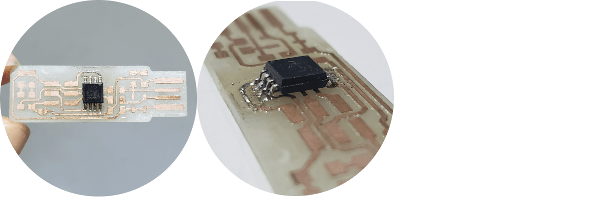
Make an in-circuit programmer by milling and stuffing the PCB, test it, then optionally try other PCB fabrication process.
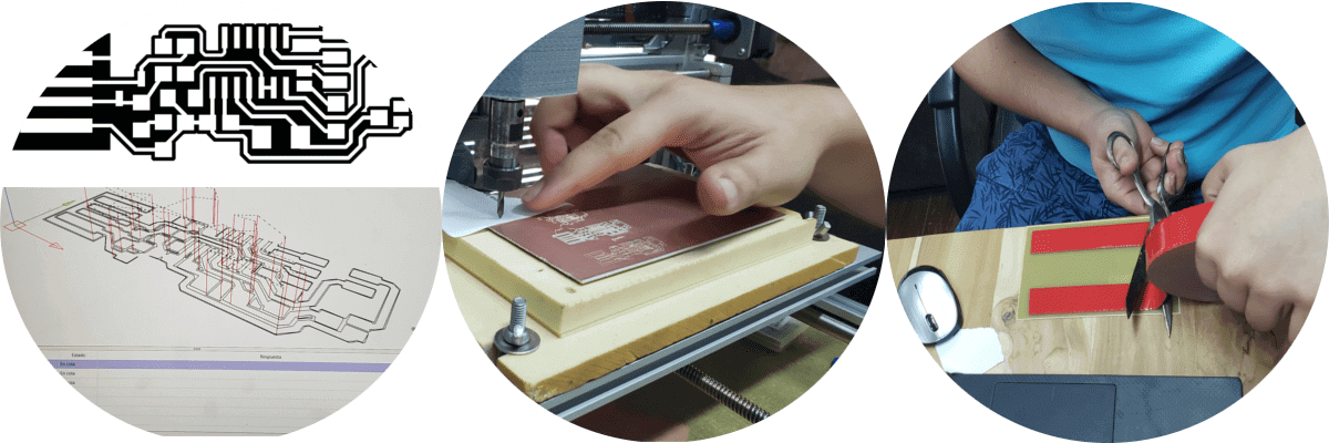
After working with the first pcb, from which we were able to cut all 4 boards in the group, we ran out of the machine for a few weeks due to firmware issues. In this period of time the plates were not touched anymore, until the time the machine returned improved thanks to the tutor, even with new software, from this moment I began to look for the work plans and it turns out that we did not find them, so We made the decision to take another model from the Fab Academy section to continue the project.
We proceeded to fiddle the new configuration, which is much friendlier than the previous one and we were able to cut the new plates in less time and more easily than the previous ones, for which the .png files corresponding to the interior and exterior parts were downloaded of the new model (both are at 1000 dpi).
The download address is: Zaerc's
FabTinyStar page

The next step is to go to the fab modules to process the files and generate the corresponding gcodes:
Fab modules / image (png) / fts_mini_traces / output format / G_codes (.nc) / process / PCB_traces (1/64) / calculate / save; In this sequence the factors that we changed were:
Output = spindle speed (RPM): 10000 @ 1000

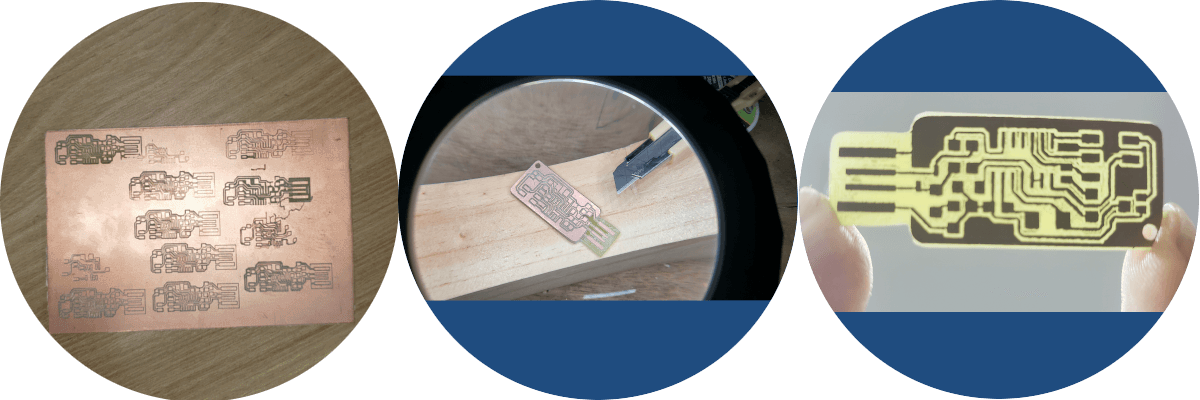
And so we come to this result and collect the components to weld the components, but not before going through the continuity test...
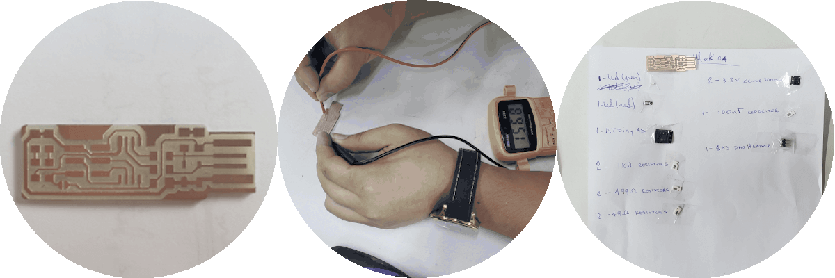
These components are:
- 1x ATtiny45.
- 2x 1kΩ resistors.
- 2x 499Ω resistors.
- 2x 49Ω resistors.
- 2x 3.3v zener diodes.
- 1x Red LED.
- 1x Green LED.
- 1x 100nF capacitor.
- 1x 1x 2x3 pin header.
- Once all the components were available, we proceeded to prepare the work area.
- The welding equipment started.
- I looked for a sponge moistened with water.
- The soldering station was prepared, however switch to a mini soldering press because it required support on the arms (use the edge of the work table) to hold the pulse using the station magnifier.
- Tools requirements Soldering station:
- Soldering station or soldering iron (Micro tip).
- Soldering lead wire tweeze.
- Desoldering wick.
- Three-arm workstation and magnifying glass lens.
- Multimeter.
- After a while, I managed to solder the chip.
- After this day, quarantine was decreed by COVID-19 ... and we are waiting...
Inconveniences - Delays
The delay in this week is due mainly to the repair of the equipment and that we did not want to solder the components, despite the fact that we could burn the pcb and not have how to cut a new board.
In addition to the above, we have been greatly affected by the quarantine decreed by COVID-19.