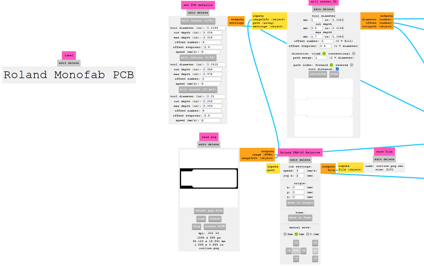
Electronic production 2.0
Update 06/07/21
Group assignment
here you can go to de Lab page to see the group assignment
Individual assignment
As always you can check all of the links at the end under "links and references"
This is a Re-do on this week assignment if you like to see what i did on facademy 2020-2021 you can check this link also avaliable under "links and references".
This assignment has diferent parts
- New Gen ISP
- My weapon of choice
- Bill of materials
- first method :modsCE
- Second method: Vcarvepro 9
- Programming the ISP
- Programming Quentin's programmer
- Links and references
New Gen ISP
And all of the links will be together under the "links and references" part of this page
With another year comes another attempt to finish my Fabacademy2020 journey.
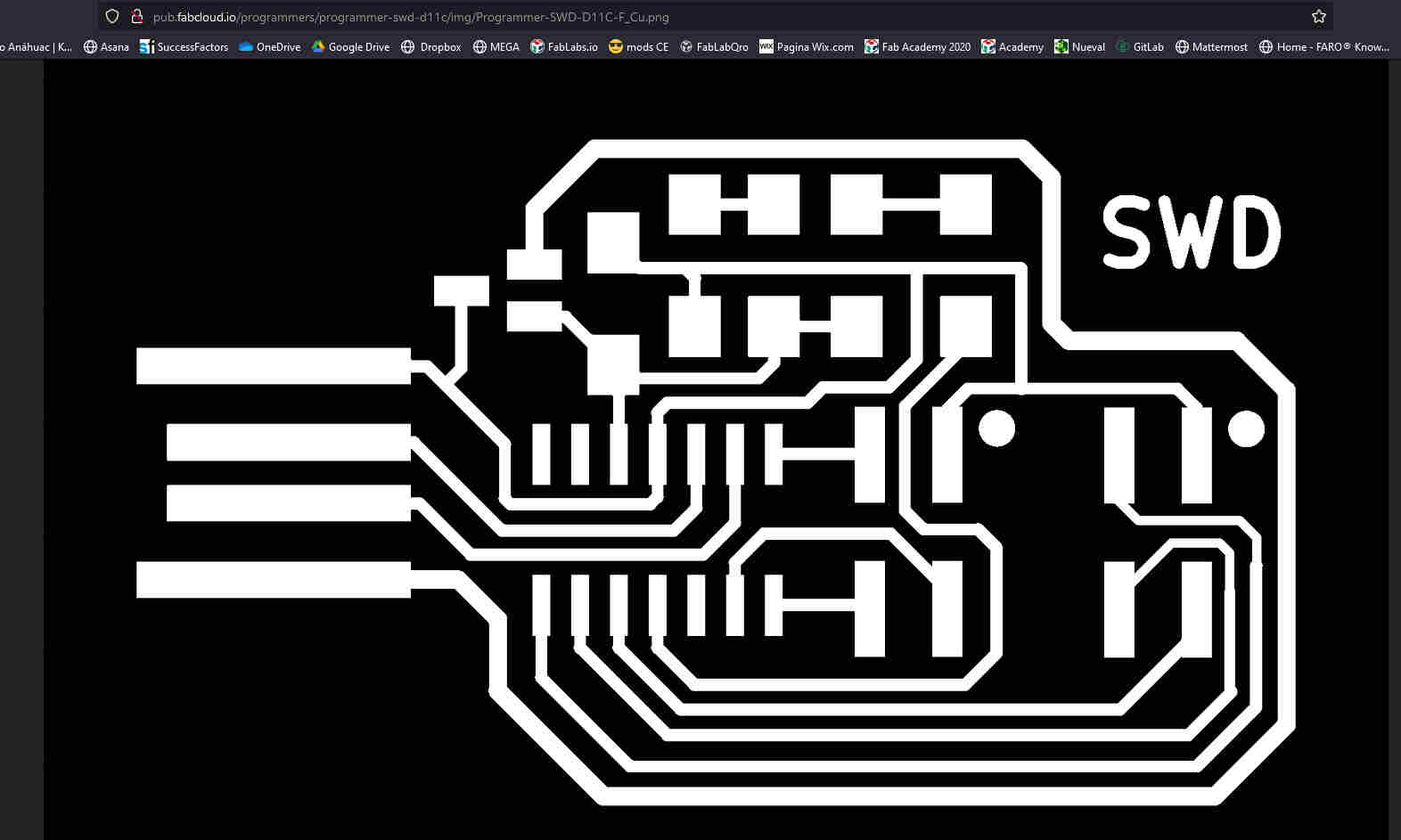
This year we had to made a programmer using the SAMD11C and the new attiny gen.
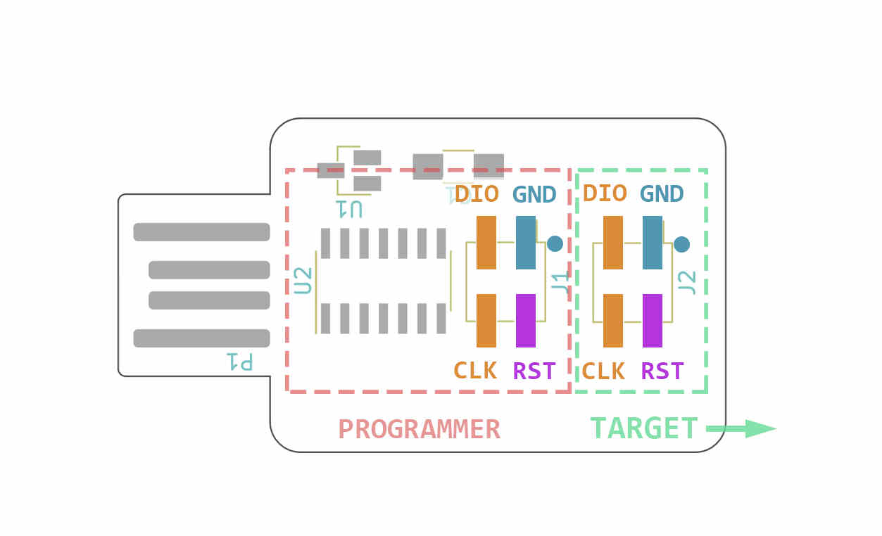
i've chosen the quentin's SWD programmer because it looks simple enough for a beginner like myself
My Weapon of choice
Altough i've used mods for this assignment. i will not use it in other board.
For this tutorial i've made the brian's version of Fabtinny45 ISP and used a raspberryPI to programm the MCU using an Atmel-ICE and following brian's tutorial
you can see directly the tutorial on that respective part.
Bill of materials
Brian Does a better job explaining the details on his board i'll only repeat what he has done.
- 1x ATtiny45 or ATtiny85
- 2x 1kΩ resistors
- 2x 499Ω resistors
- 2x 49Ω resistors
- 2x 3.3v zener diodes
- 1x red LED
- 1x green LED
- 1x 100nF capacitor
- 1x 2x3 pin header
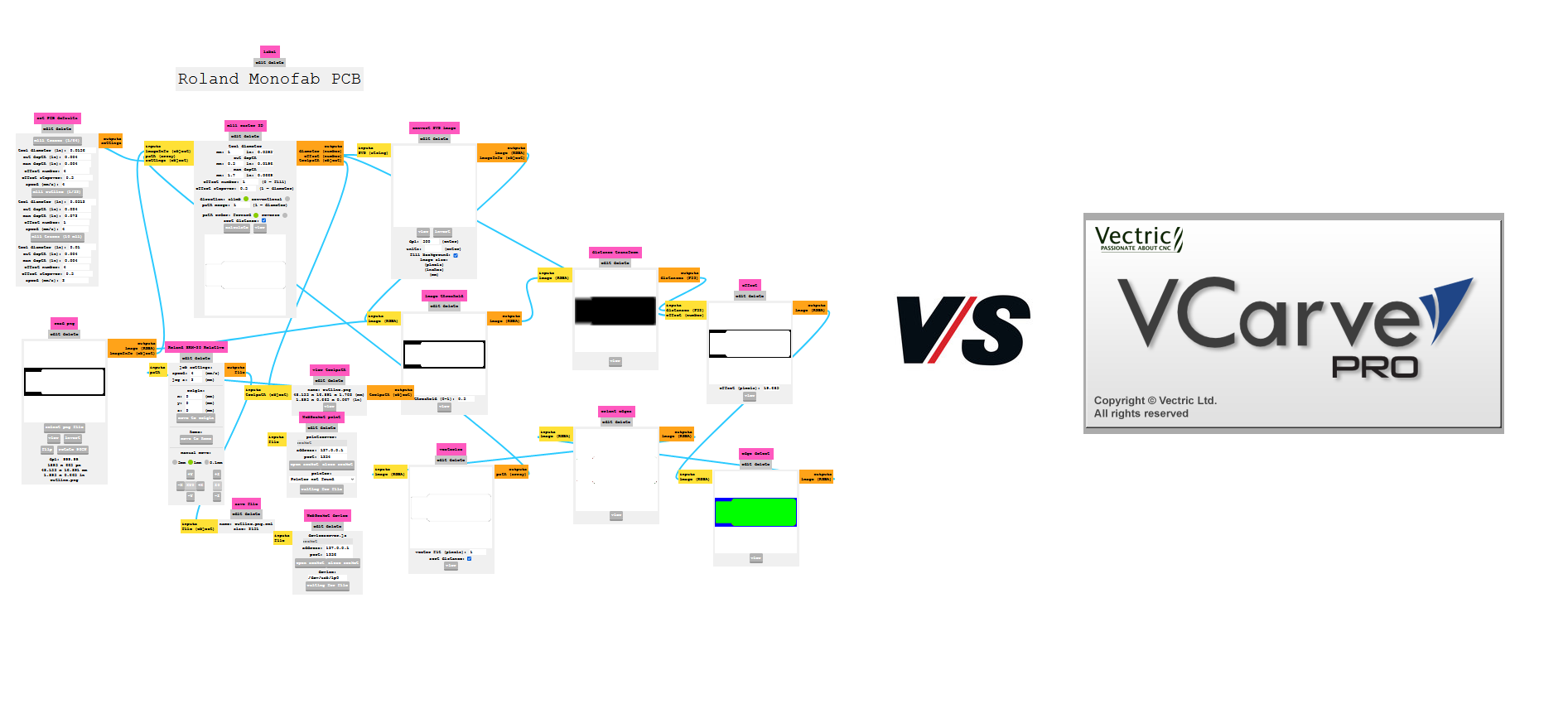
First Method: ModsCE
first you enter this text on the browser
and you'll see a white canvas and an icon that will tell you how to navigate
right click on the canvas will open the window on the image above. you'll have to select "program"
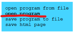
here you have to select "open program"
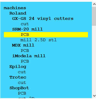
Here you'll have to select "PCB" under SRM-20 mill
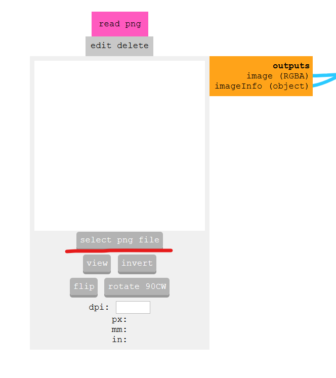
the first thing you'll need to do is to insert brian's traces png into mods.
you do this by clicking on the "select png file" on the read png block
HERE You can download brian's traces file
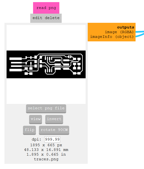
once loaded it should look like this.
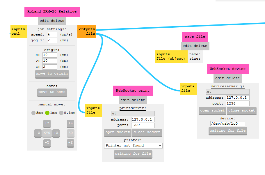
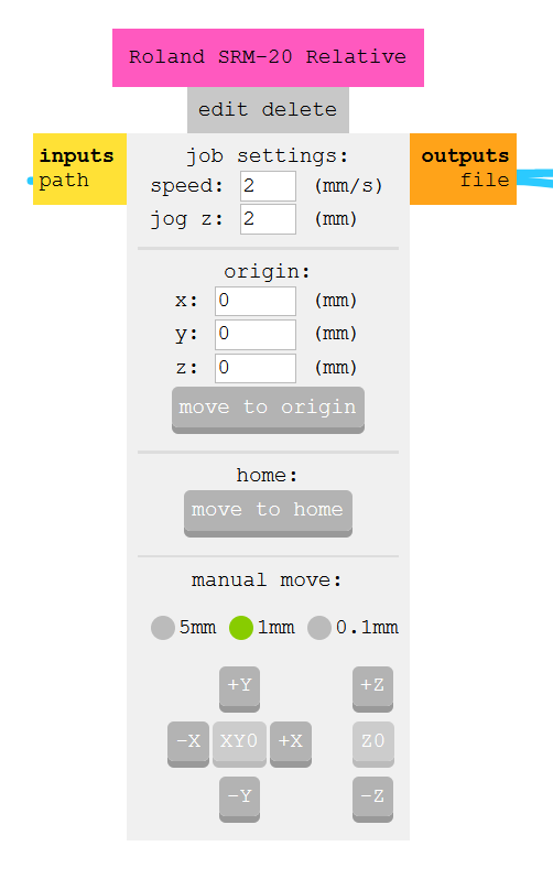
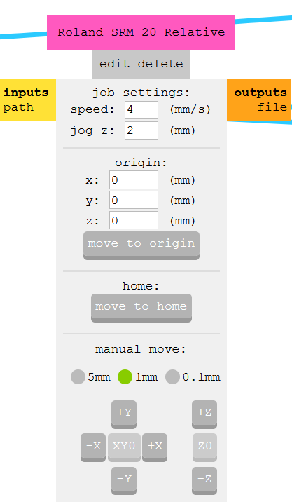
Now, let's take a look on the Roland SRM-Relative block.
and then click on "file" tag on the input of the WebSocket device block.
Then to conect the output from the SRM-20 block to the save file block.
first you need to make click on the "file" output tag on the roland srm-20 block.
and then other click on the "file" input tag from the save file block.
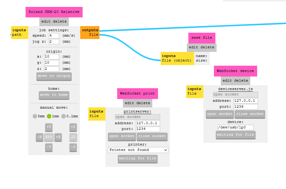
when it done it should look like this.
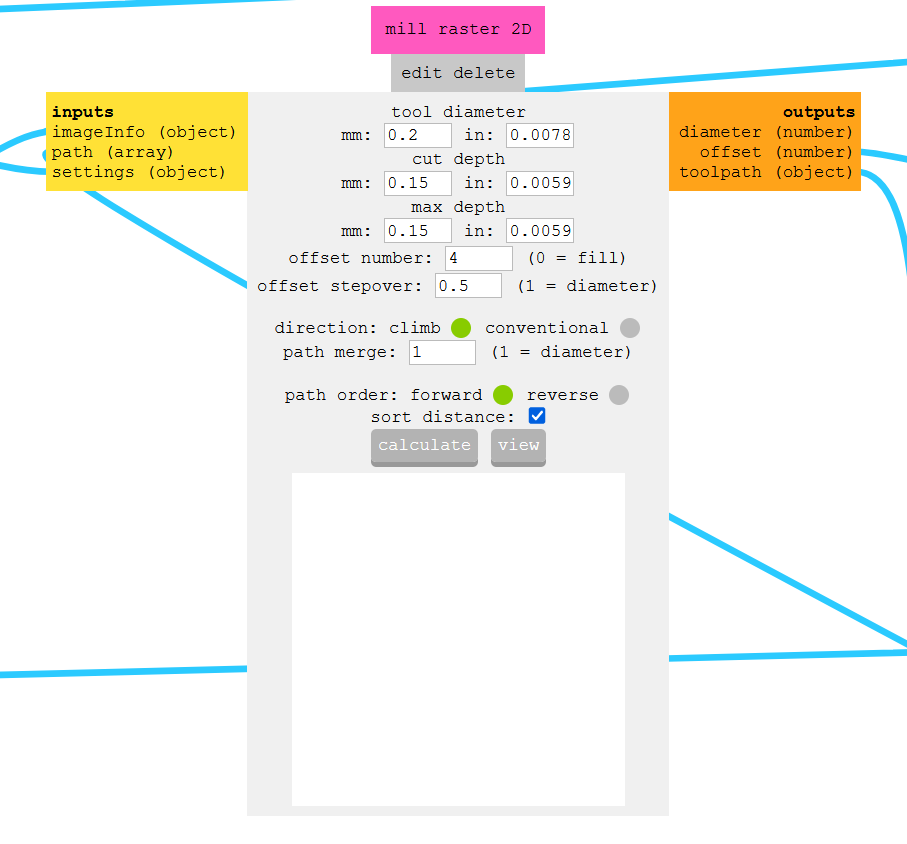
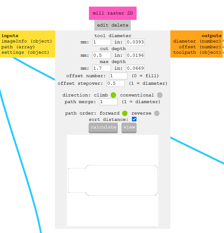
this are the settings i used for the endmill we have in our lab.
this is the settings i used for the speeds and feeds
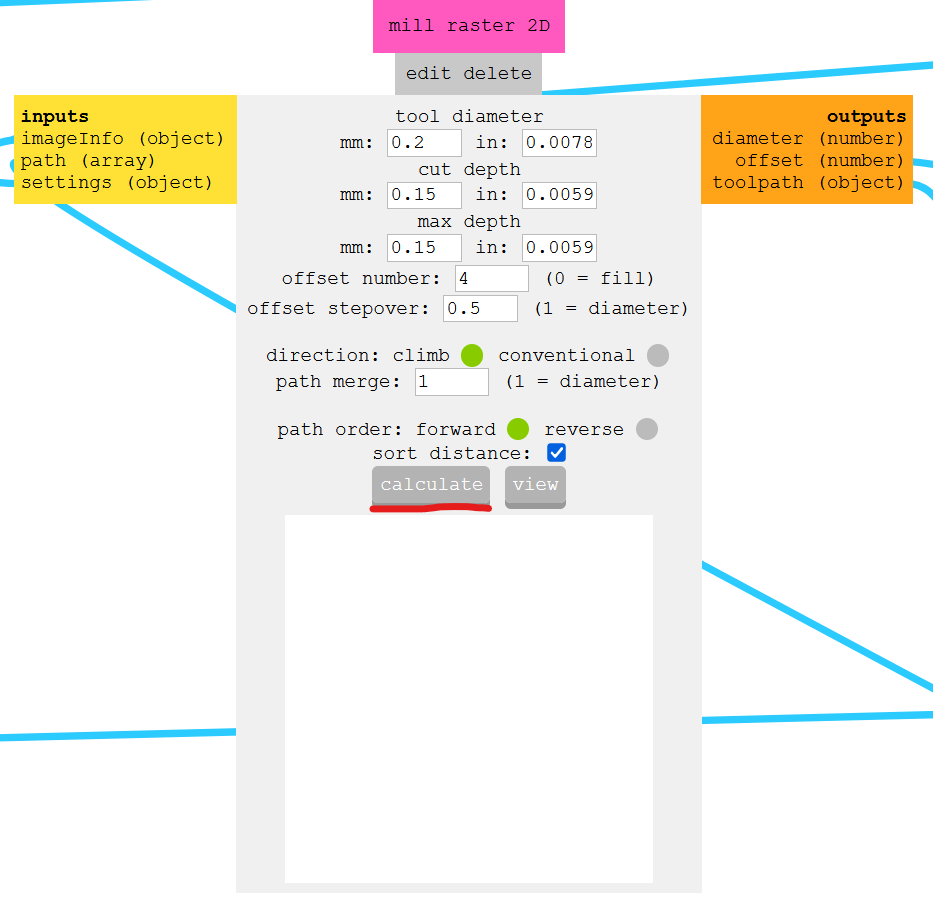
Now click the "calculate" button on mill raster 2D block.
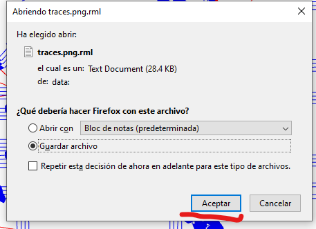
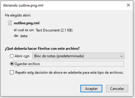
you will be prompted with this window asking to save the file on your hard disk.
HERE You can download the outlines file from mods
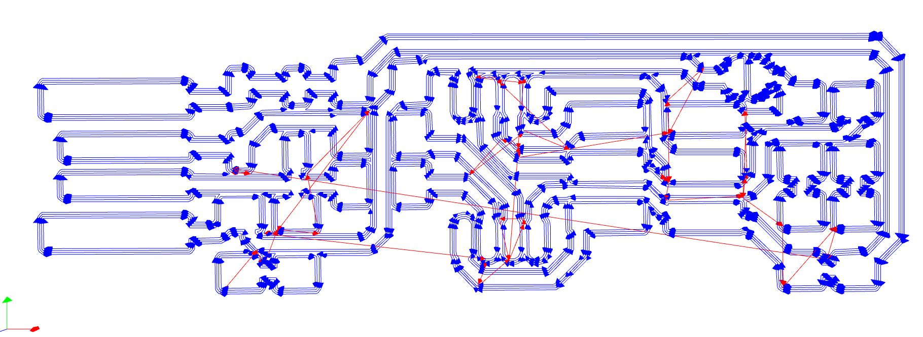
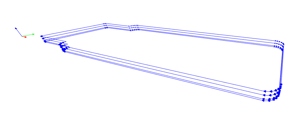
then you can check the preview for this operation.
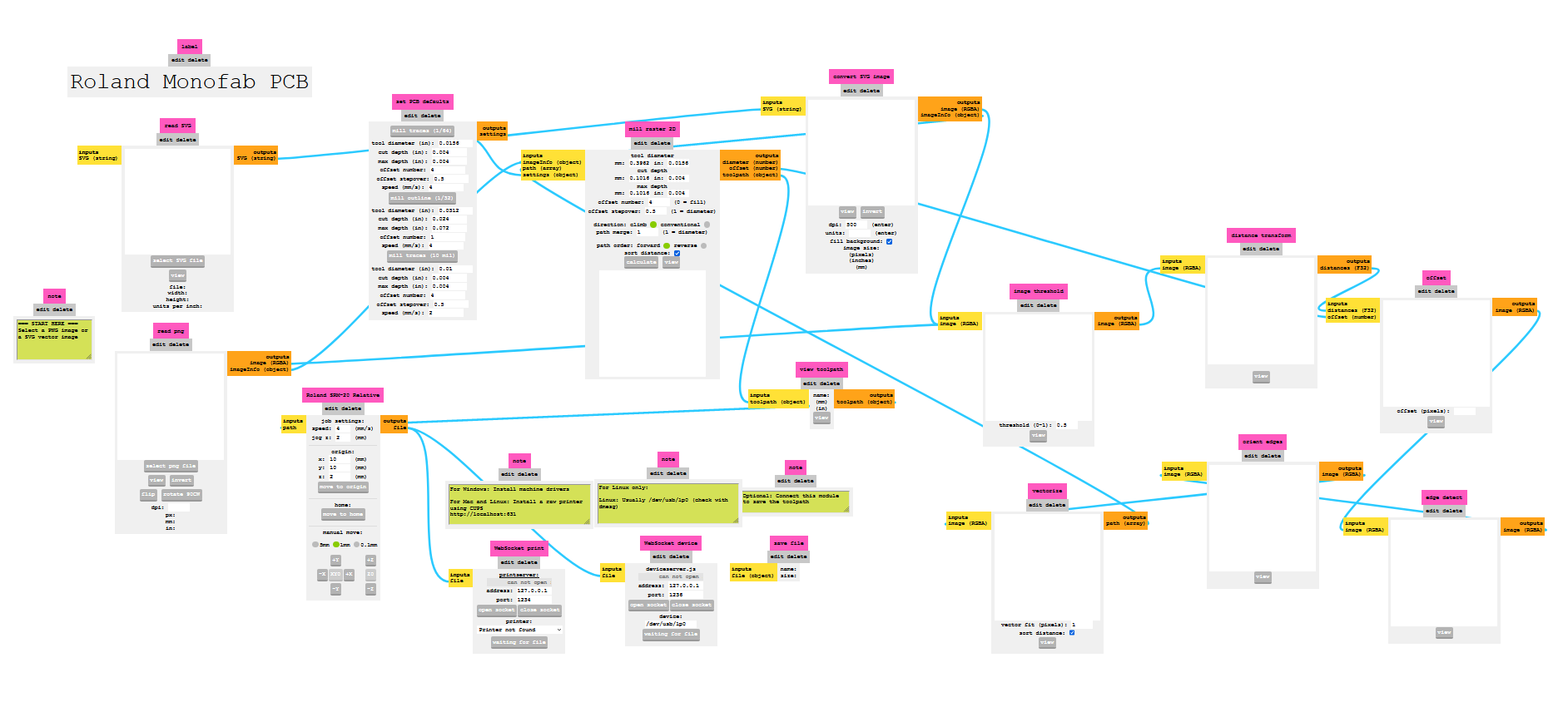
this is the overall vew of all the blocks conected.
now let's repeat the steps for the outline file
HEREyou can download my outline roland file.
You can download brian's outline file/a>
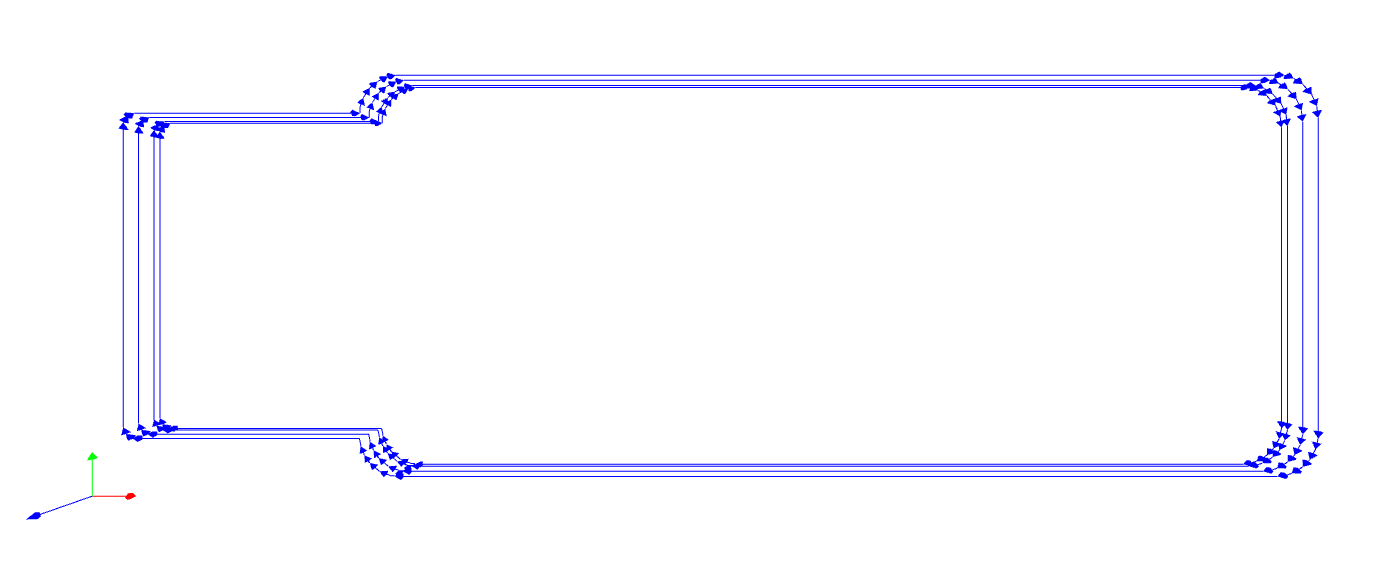
This is the preview you'll spect to see.
it's jus one line with diferent thicknes steps
this is the overall view of all the blocks conected
the parameters i used on the 1mm diameter endmill we have in our lab
the feed rate on the 1mm endmill
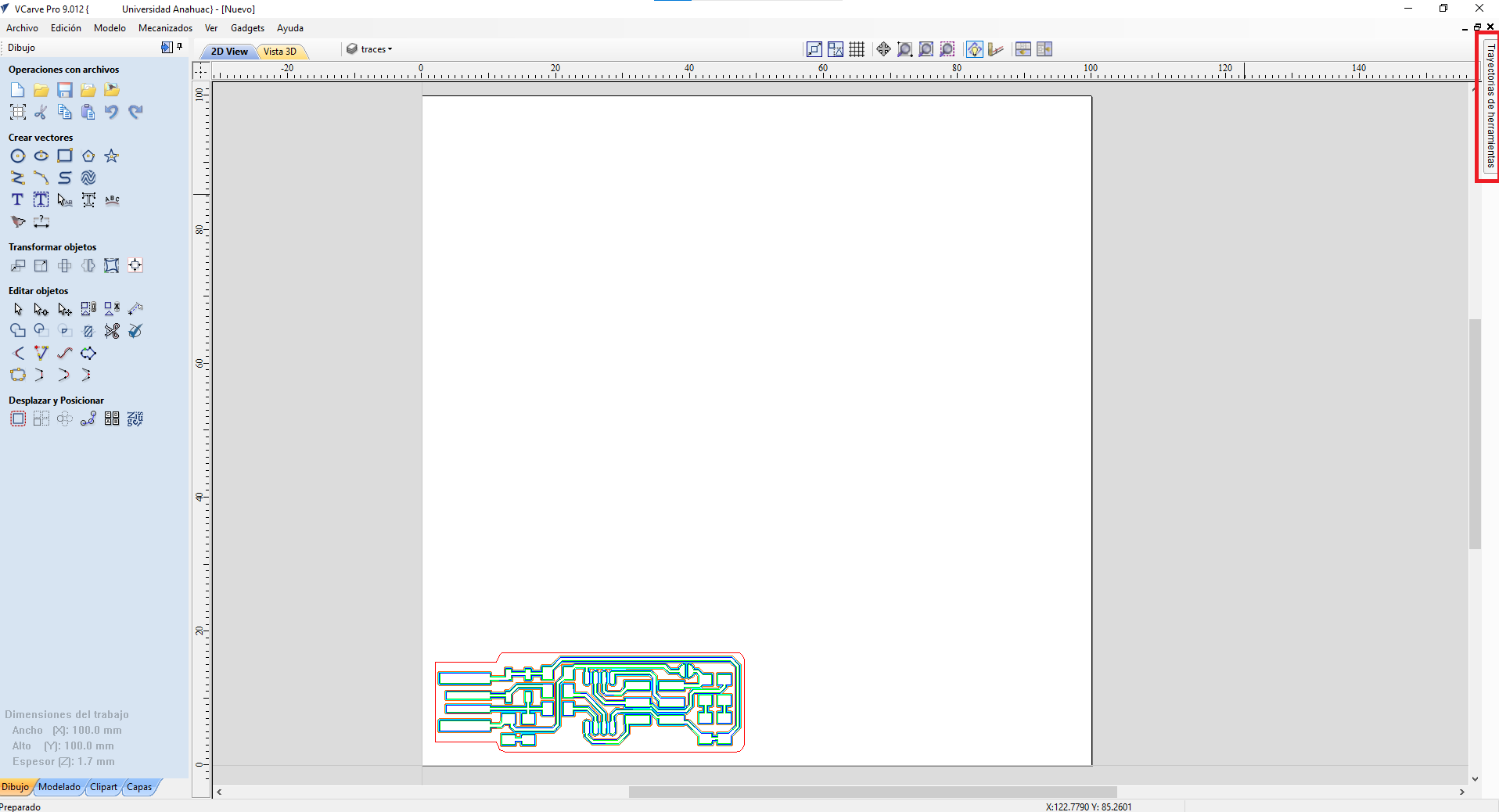
Second method: VcarvePro
Of course this setting will depend on the machine, the material and the endmill used.
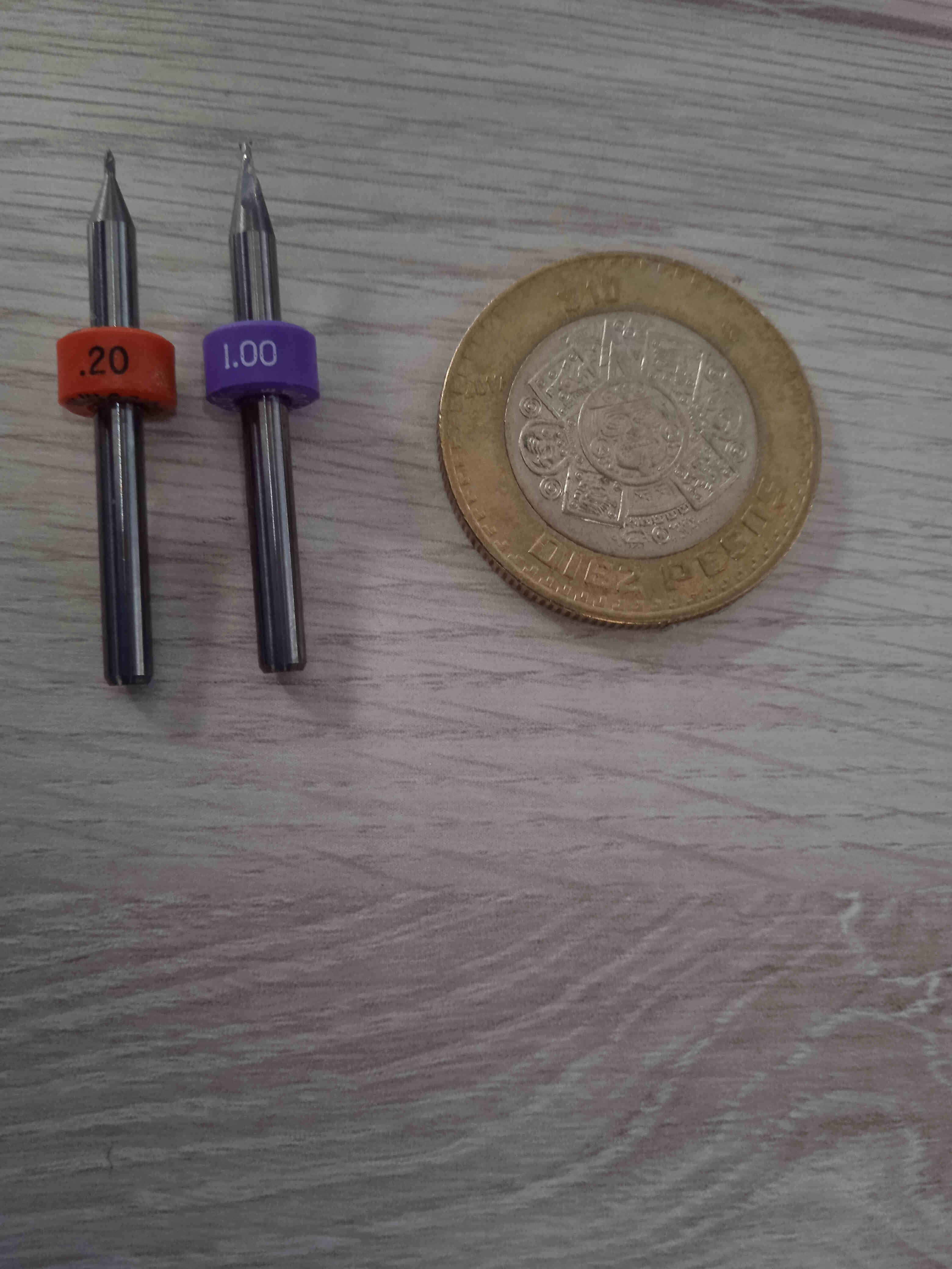
This are the two endmills used for both modsCE and VcarvePRO.
HERE is the link to buy the 0.2mm endmill
HERE is the link to buy the 1mm endmill
HERE If you wish to install the vcarvepro software for yourself.
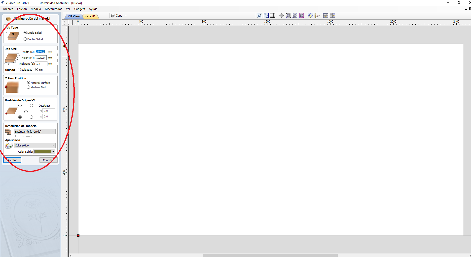
the STOCK material dimension and caracteristics tab.
Once you click accept "aceptar" button.
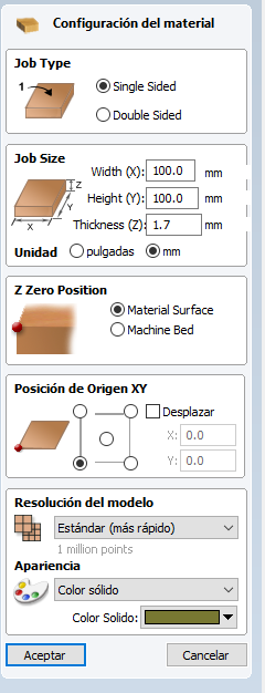
It will change into the drawing tools tab "dibujo" at the bottom of the tab.
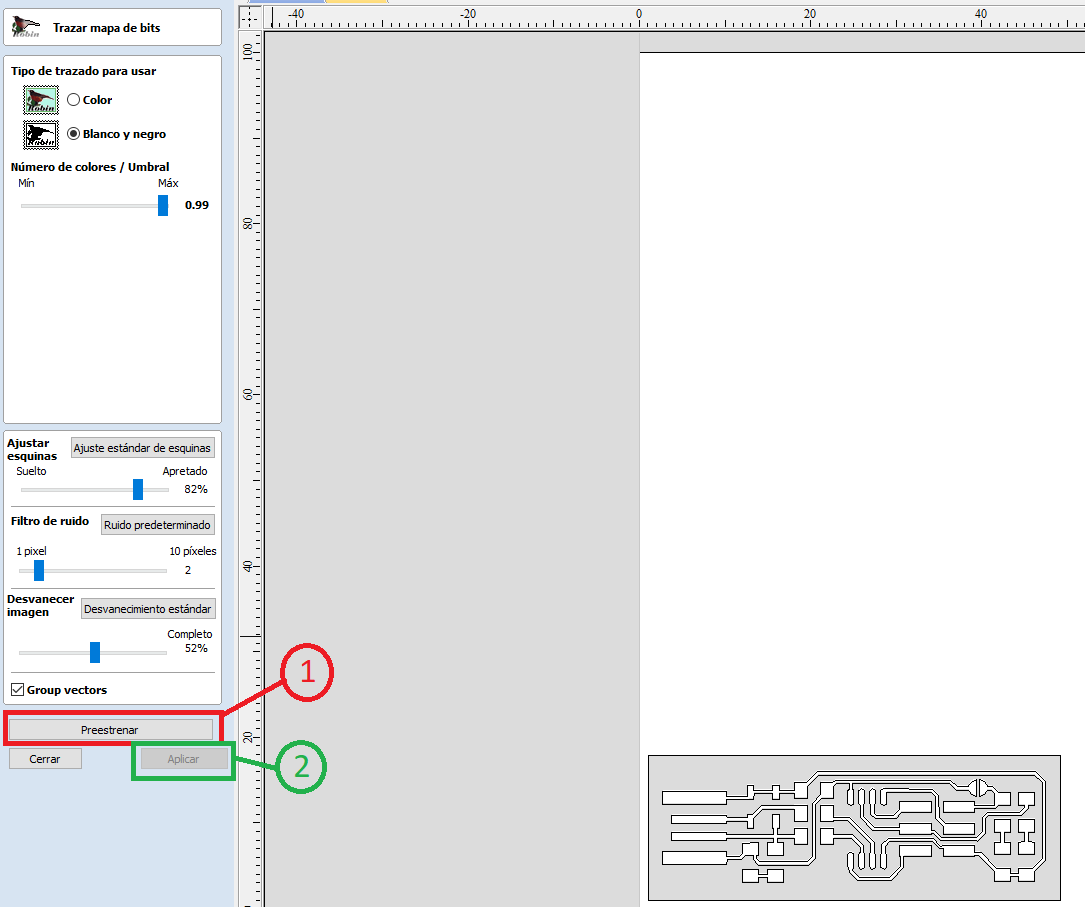
the first thing we need to do is to import our images and convert the "PNG's" into curves.
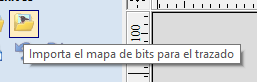
we import images from our HDD from the button called "importa el mapa de bit para el trazado"
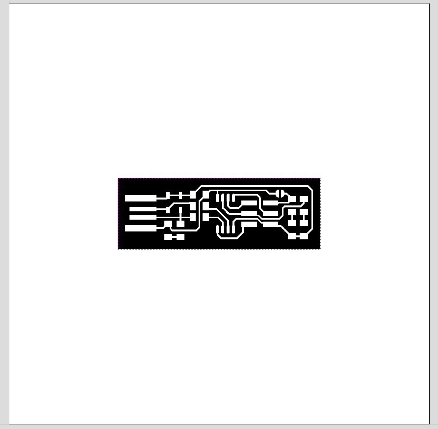
i uploaded both of brian's files.
automatically sends them to the center of the stock.
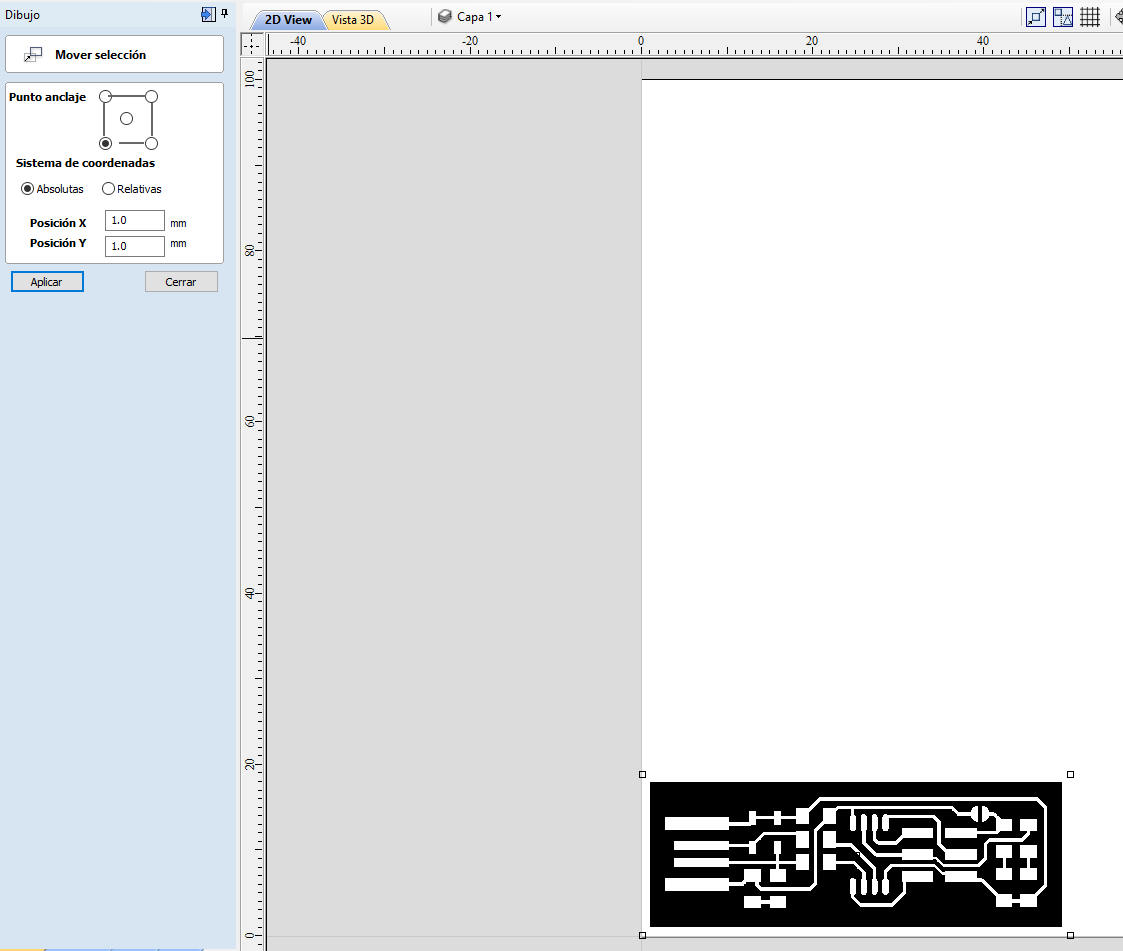
then type a 1mm in x and y direction under absolute coordinates.
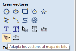
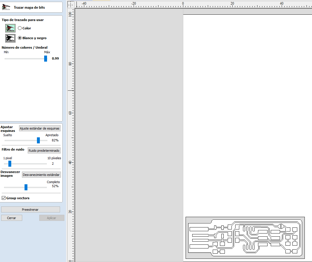
the "adapta los vectores al mapa de bits" button will create the curves from the bit map image.
once you hit click it will open the vectorization tool on the lef side of the screen.
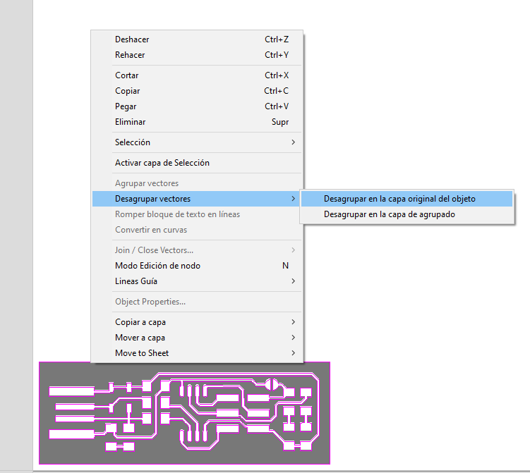
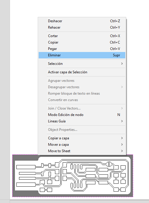
Then eliminate the outer contour that you won't need
or simply click on the line and hit the delete key on the keyboard.
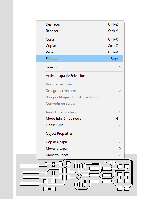
eliminate the bit map from the traces.png file
again right click/eliminar or delete key on keyboard
i used the same settings to convert the curves from this image as well.
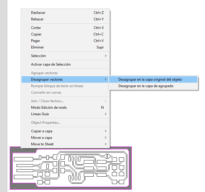
let's repeat the process to delete the unnesesary objects
delete the outline of the image
3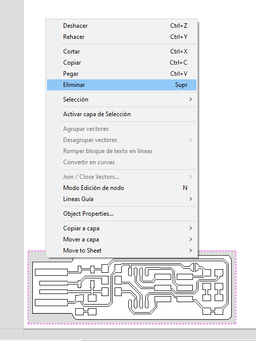
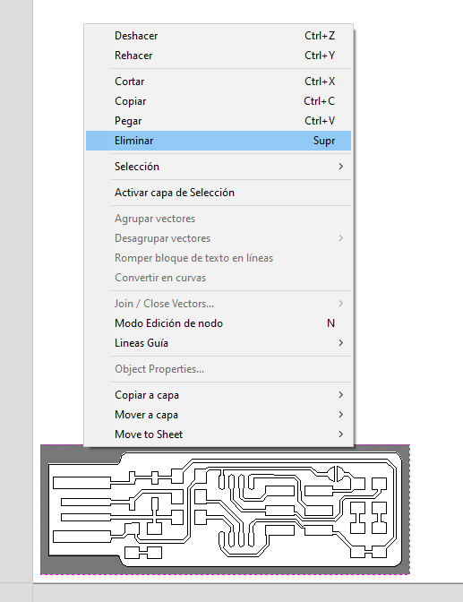
delete the ouline.png bit map from the stock to leave only the curves.
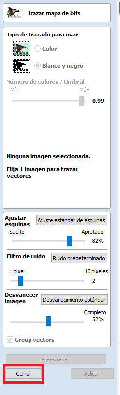
close the vectorization tools window bi clickig "Cerrar" close button
this step is completly optional but it helps a lot when dealing with larger pcbs files.
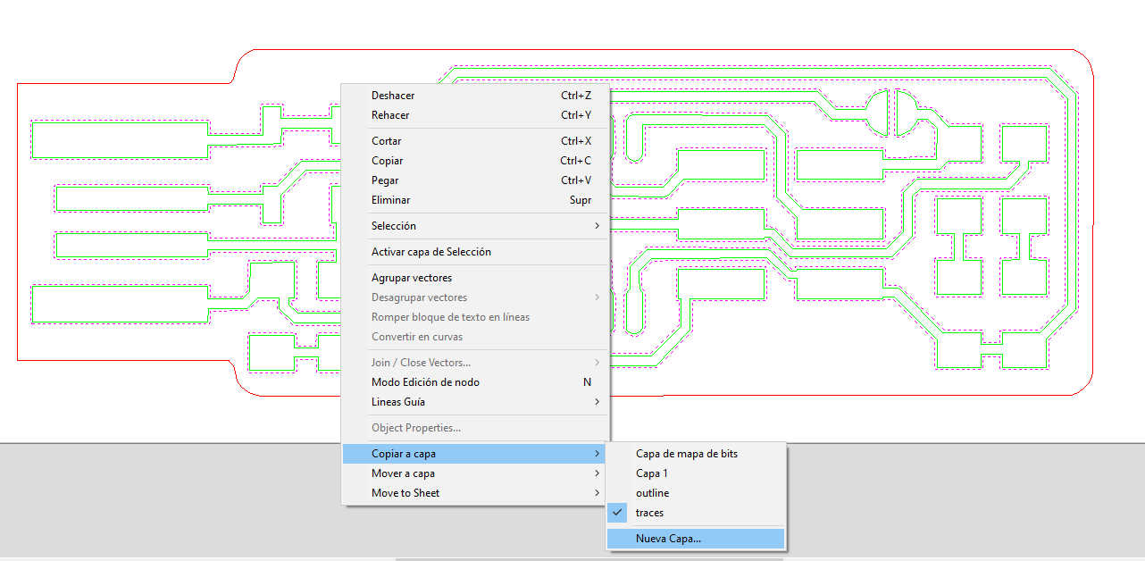
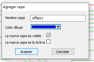
let's create new layers for all of the curve groups we will need.
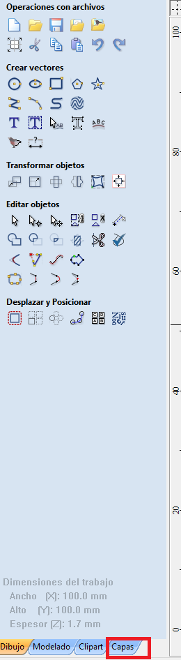
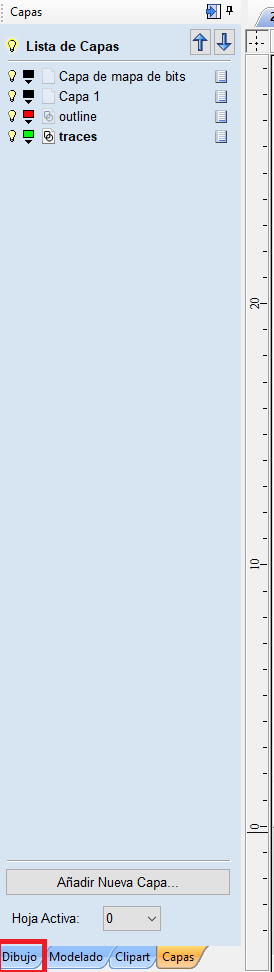
first click on the "capas" layer tab at the bottom of the screen
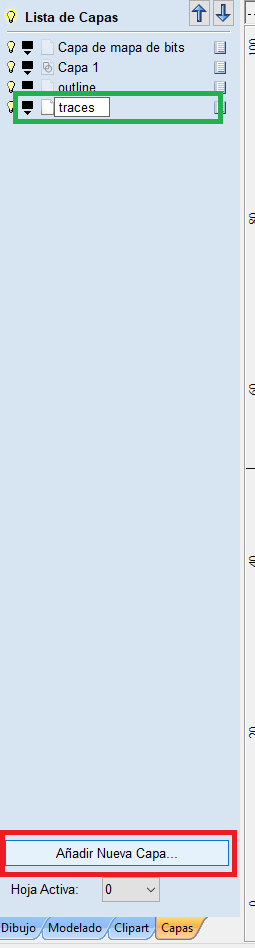
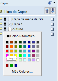
click on the black rectangle (it will change depending on what color you choose)
i found extremely handy to give diferent colors ot every layer.
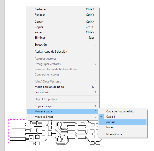
change the curves to their respective layer
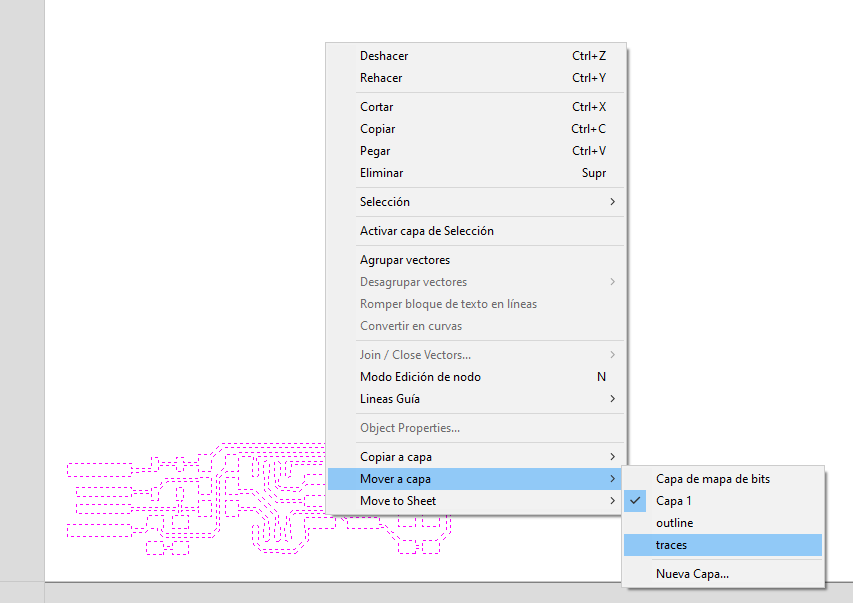
right click/mover a capa/"selecciona la capa" right click/move to layer/"choose the layer"
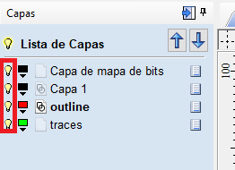
now let's hide the outline clicking on the lightbulb over the desired layer
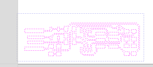
click and drag to select the rest of the curve (that will be our traces).
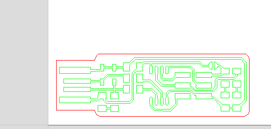
at the end it should look like this
Now it's time to manually create the offsets to the traces.
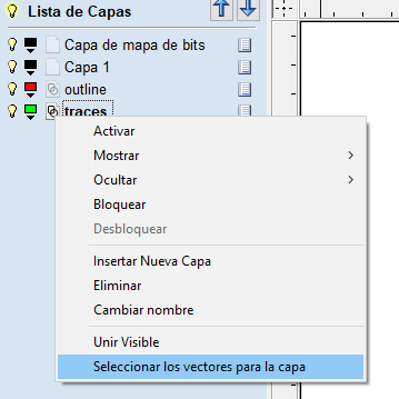
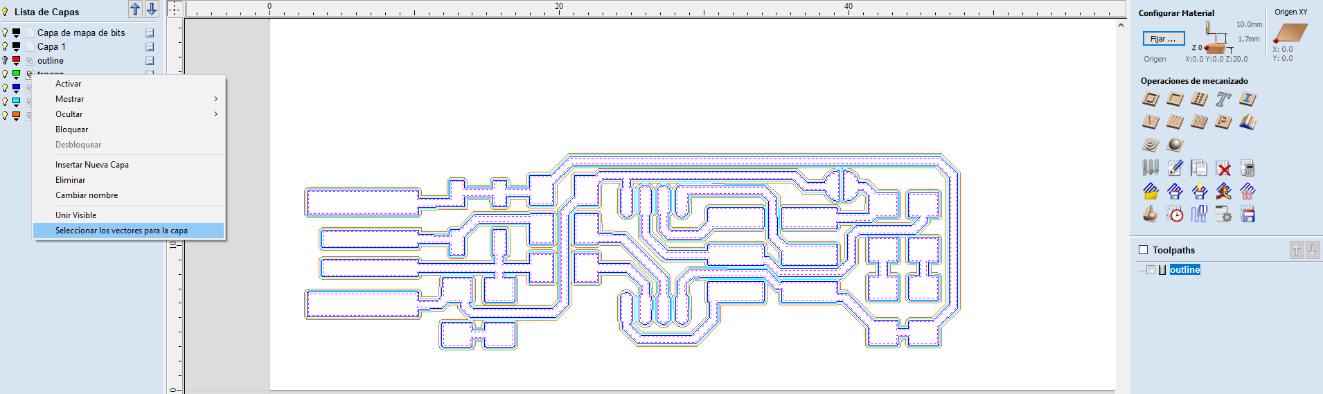
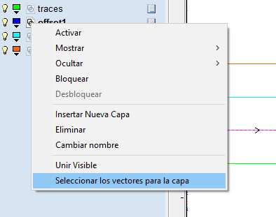
right click on the layer of the traces
choose:"Seleccionar los vectores para la capa" so select all of the curves within that layer.
go to the drawing tools tab at the bottom.
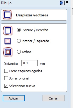
now it's a good time to create one layer for each offset.
choose a name and a color to each layer.
and repeat the steps from the *** mark on this tutorial.
until you have the offsets you like to process.
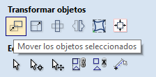
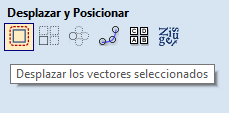
the pin button is on the upper right side of the tab.
but we can also do a "raster-like" carving called pocketing
holes with a drilling operation
open curves carving (used in sign making with a V-bit ussually)
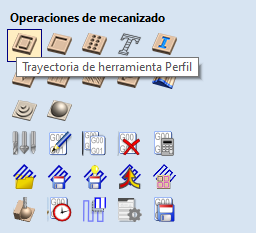
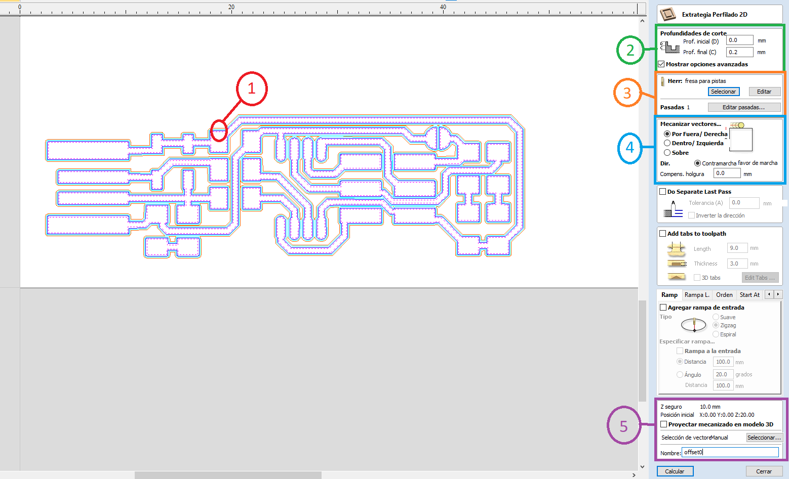
Click on the "trayectoria de herramienta de perfil" button in the pictue above.
let's make the cuting operation first.
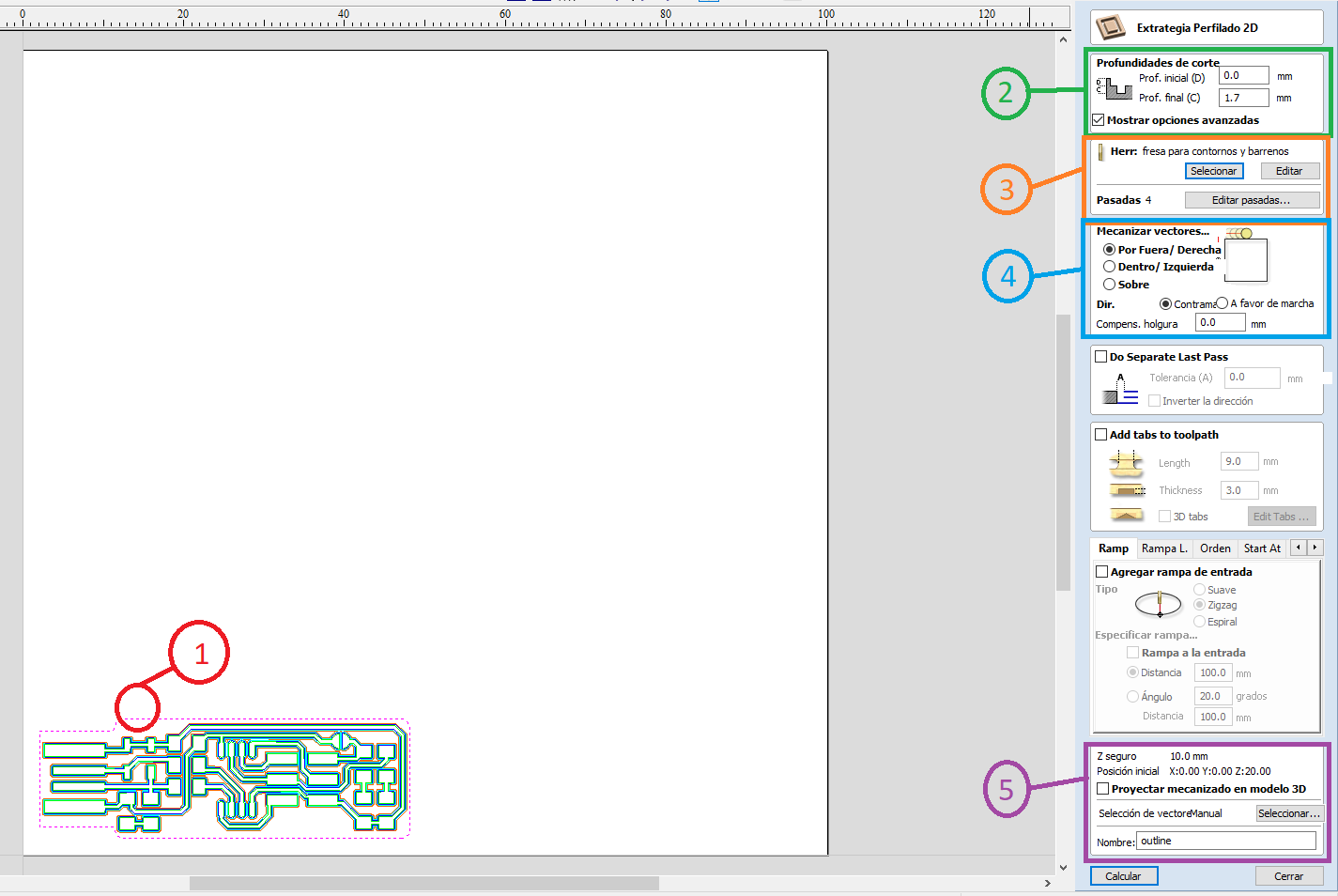
the numbers on the picture above correspond to the numbers on the following list
- select the curve you want to process with this operation.
- define the final depth of the cut. (in this case i want all of the stock to be cutted)
- select your cutter (i have presetted my 1mm endmill you can the the parameter in the picture below)
- define where you want the operation to be made (on,over or under the curve) and the direction conventional or climb (i've found this settings to be the ideal.)
- name and calculate (set a name that will be using for the output file.) and remember to set a proper safe height (10 mm in my case)
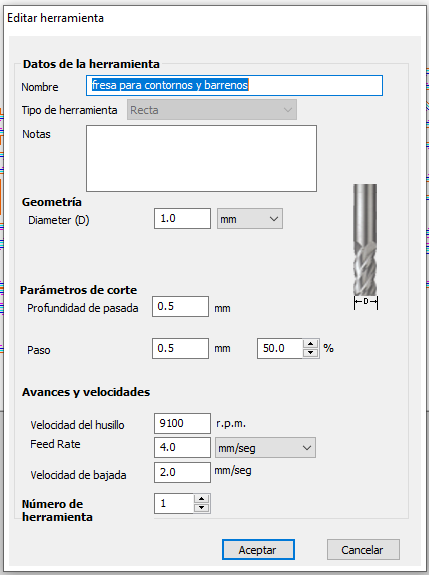
the setting on the cutting endmill
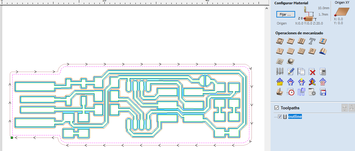
after that it shoul look like in the picture above.
and select te first set of curves to process with another cam operation.
the numbers on the picture above correspond to the numbers on the following list
- select the curve you want to process with this operation.
- define the final depth of the cut. (in this case i want 0.2mm wich ussually is the depth of the copper layer on the pcb.)
- select your cutter (i have presetted my 0.2mm endmill you can the the parameter in the picture below)
- define where you want the operation to be made (on,over or under the curve) and the direction conventional or climb (i've found this settings to be the ideal.)
- name and calculate (set a name that will be using for the output file.) and remember to set a proper safe height (10 mm in my case)
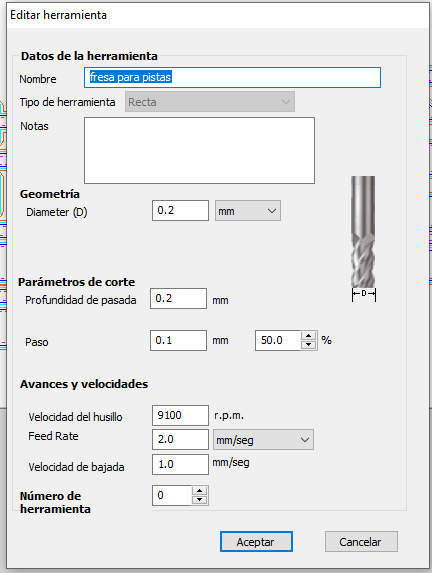
The settings on the traces endmill
Now, let's duplicate this same operation to the other offsets.
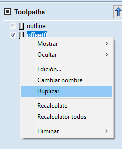
right click "duplicar" button to duplicate
repeat this until you have one CAM operation for each layer of offsets you've made.
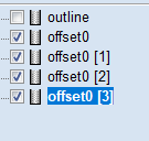
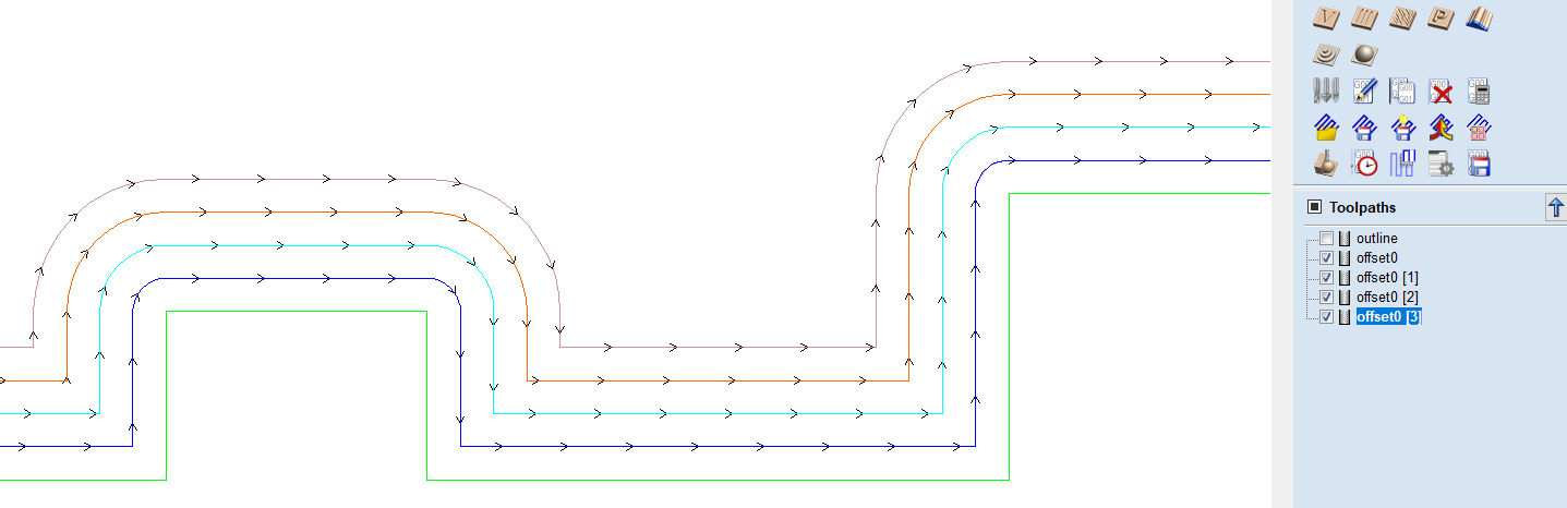
in my case i have 3 offsets and the original set called "traces".
double click on the respective offset CAM operation.
select all of the respective curves for each offset layer. like in the picture above.
again,right click on the layer and "seleccionar los vectores para la capa"
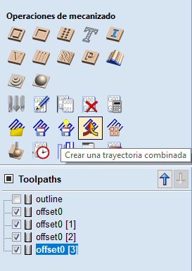
click on the "crear una trayectoria combinada" button to merge the selected toolpaths.
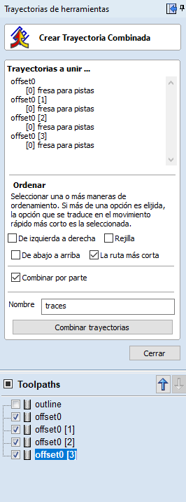
Select only the toolpaths you'll want to merge. like in the picture.
and give them a name for the final output file.
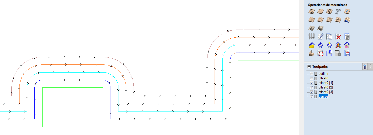
it should look like this (the merged toolpath is under the undividual cam operation that)
this is the merged operation selected.
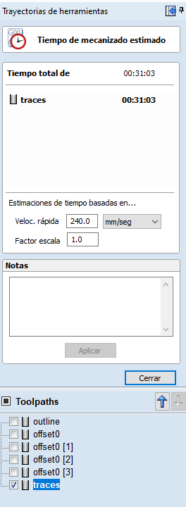
on "velc. rapida" set 240mm/seg that's the rapid speed when it's no carve.
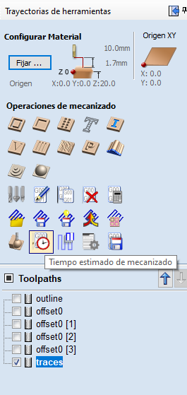
Also optionally you can simulate the operation.
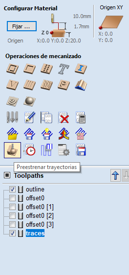
just click on the "preestrenar trayectorias" button.
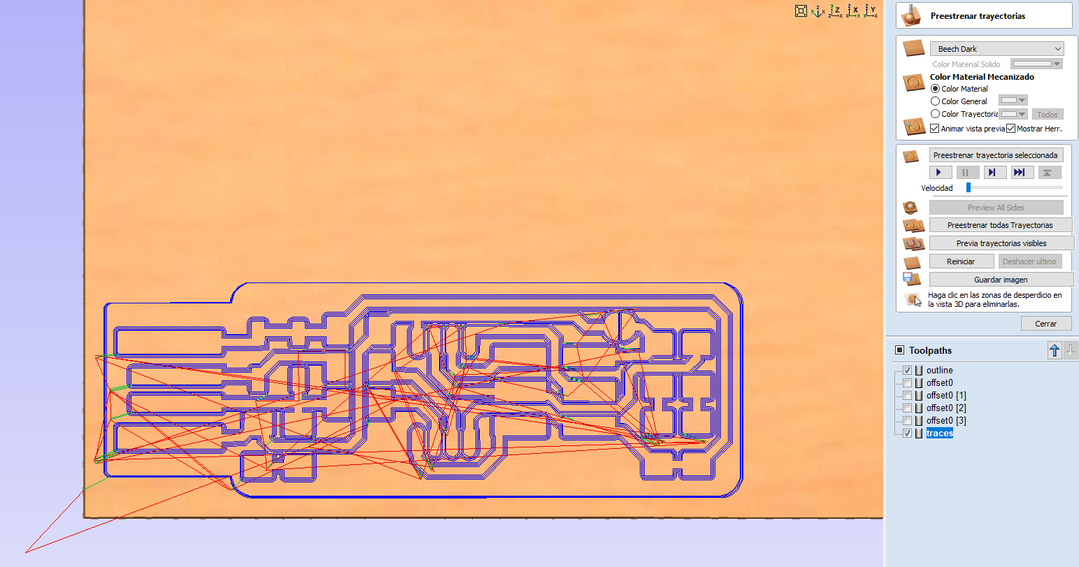
Select the check box on every CAM operation you want to simulate.
click on "preestrenar trayectoria seleccionada" button to play the simulation
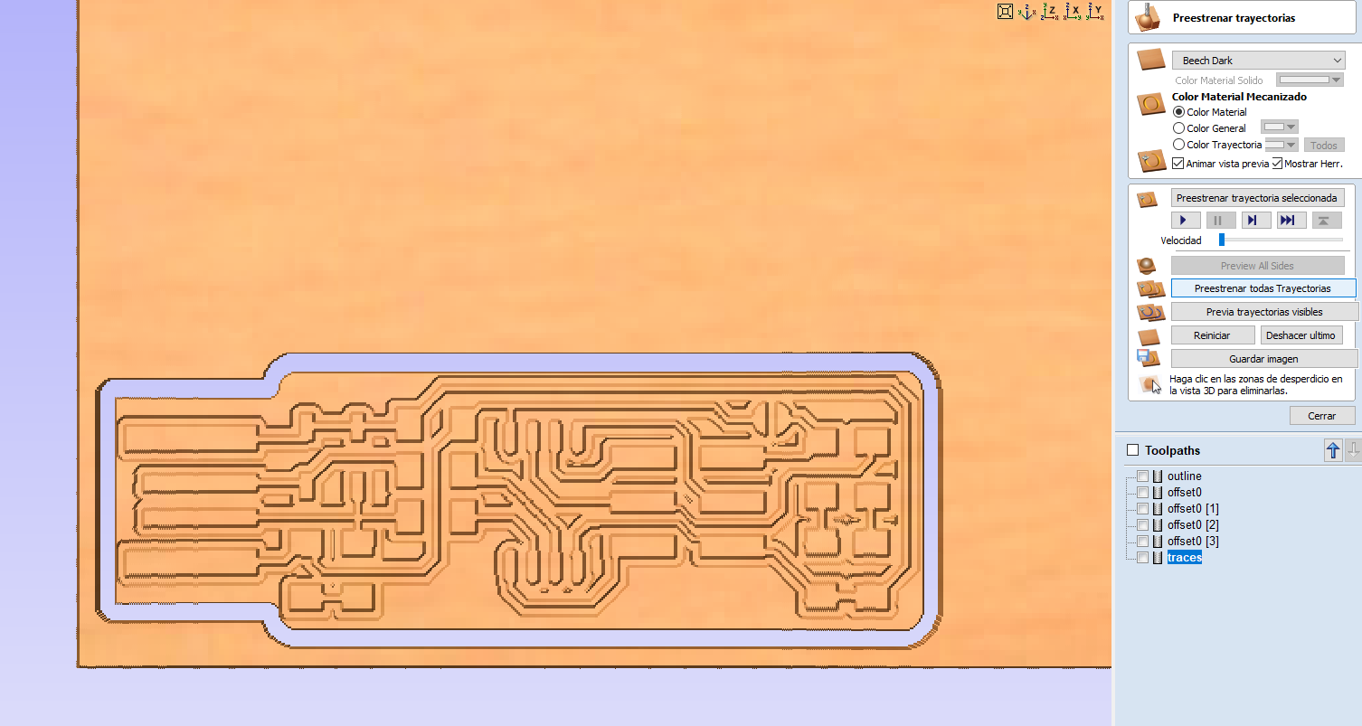
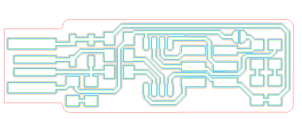
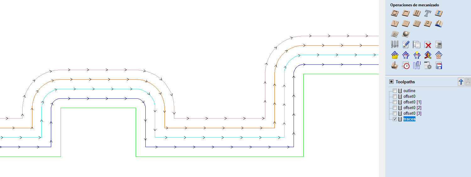
this is the simulation of the CAM
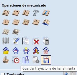
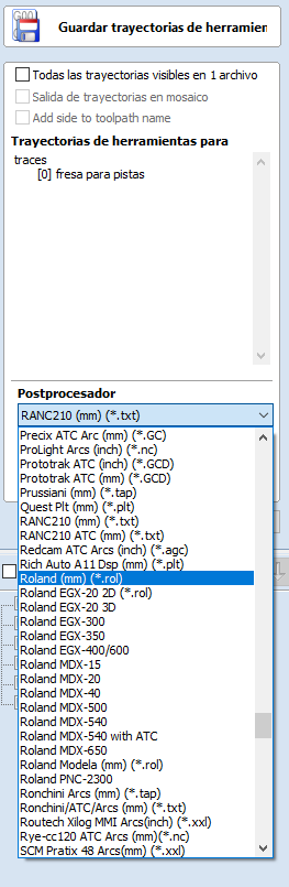
select the "Roland (mm)(*rol)" option under postprocessor and click on "guardar " button to save
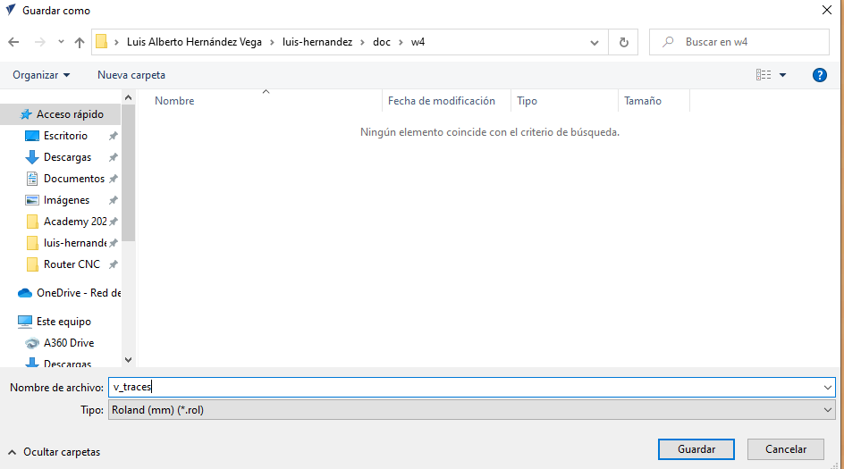
Select a location to every file for the roland.
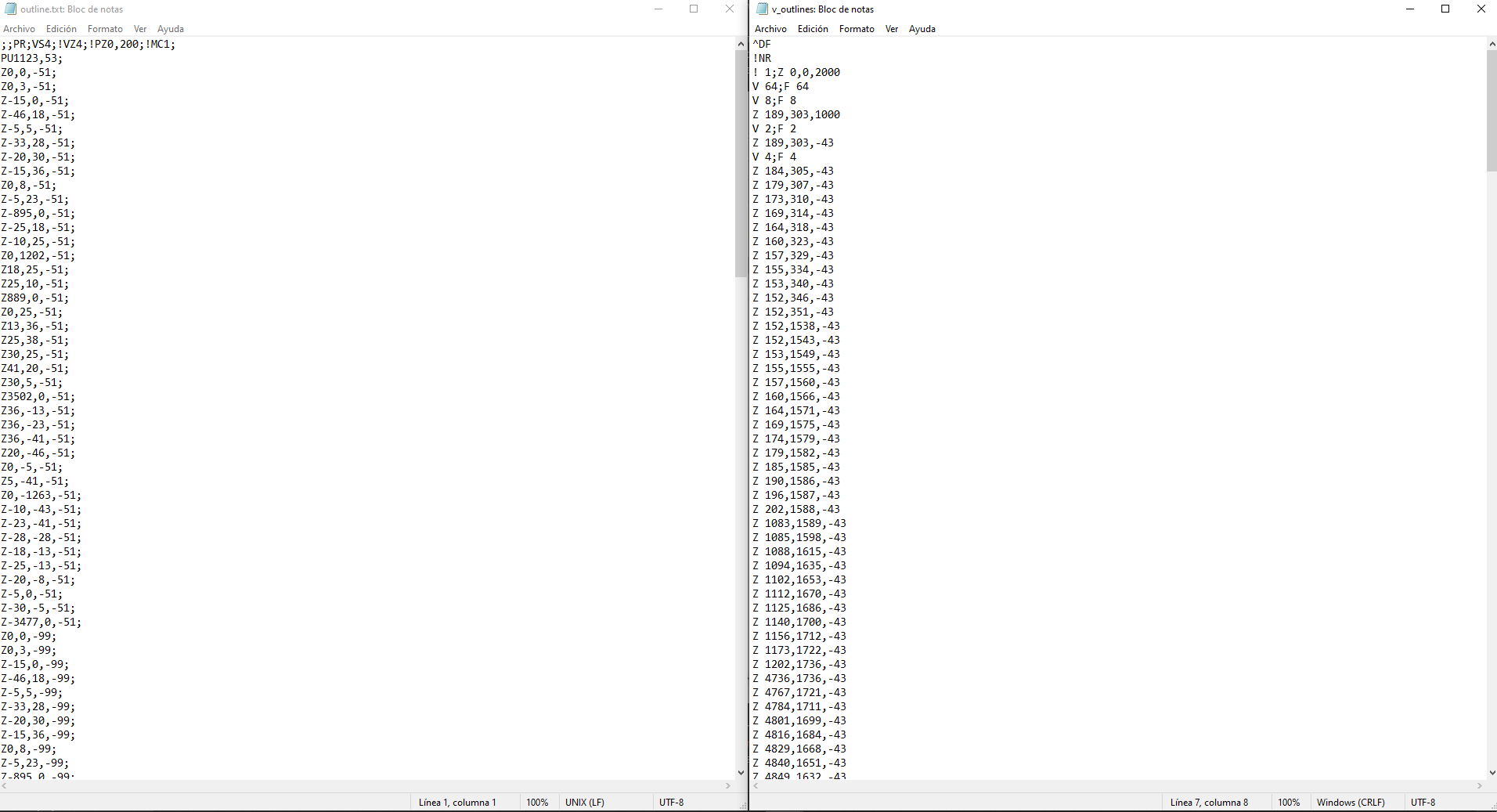
Finally this is the comparison between the two postprocessors
HERE you can download the Vcarve generated roland files
HERE You can download the vcarve editable file.
Make an in circuit programmers
Prepare the machine
Set your sacrificial layer
In order to save the roland to cut on the machine bed is necesary to make a sacrificial layer to place the PCB on and cut through MDF instead of Steel. That’s why i made my own sacrificial layer. The PCBS we have in the lab are 100X100X1.5 mm in dimesions so i cut out two 9 mm MDF about 100x100mm and glue them together using som PVA glue. Then place them in top of the machining bed using some double sided tape.
So since i used PVA glue and double sided tape i altered the new machining Surface and don’t know if it will be flat enough. Therefore i flatten out the Surface using the following method.
Set your zero on the sacrificial layer (method 1)
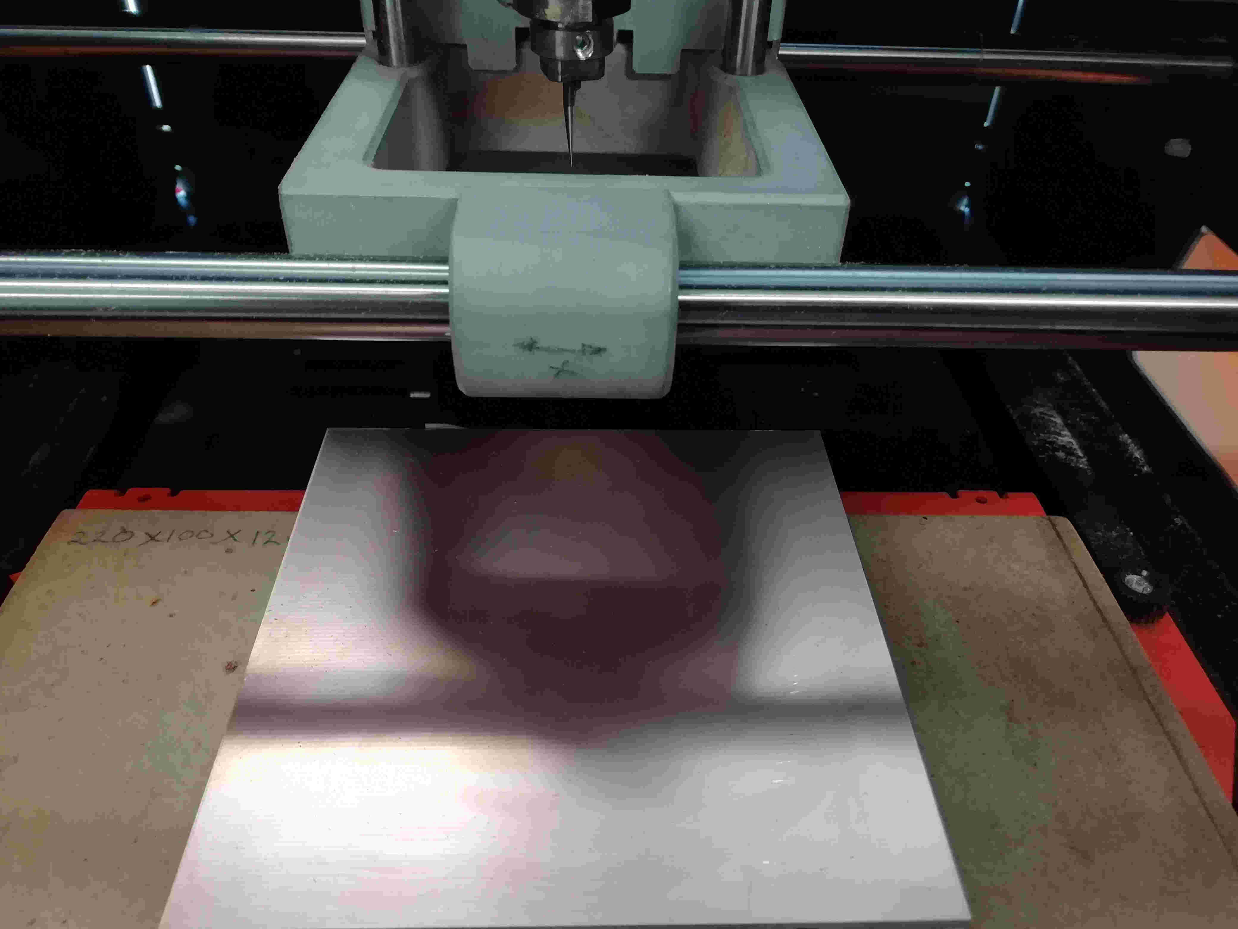
First i placed a 3 mm endmill on the SRM-20, place the machining Surface to flatten out.
 Opened the Factory software from Roland called VPANEL so i could guide the cutter to the desired place to start the cut.
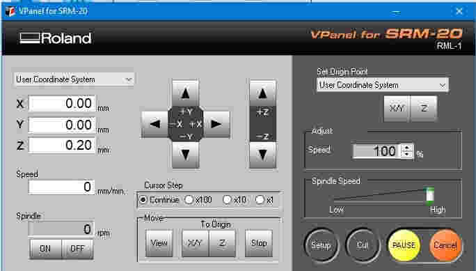
The origin of this cut will start on the lower left corner like in the figure.
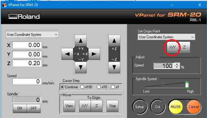
 Then clicked on the X/Y button on the right side of the VPANEL window in order to create a user origin for my piece.
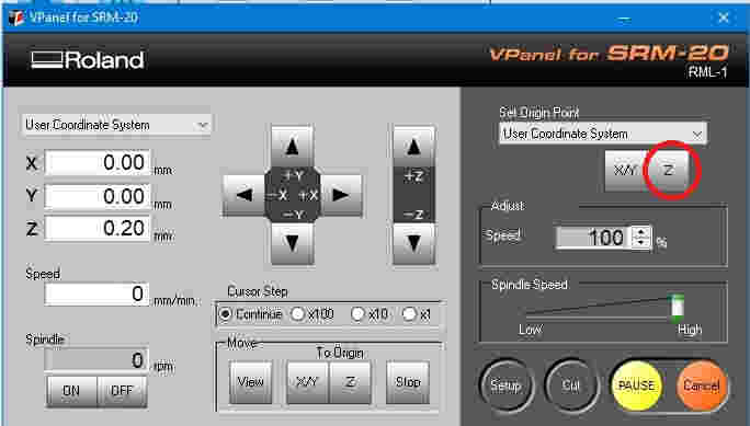
Then with some help of a Little piece of Bond paper i placed between the endmill and the Surface of the MDF i started to jog the Z axis in X10 increments so i could’nt damage the tip of the endmill and stopped until felt some fricction on the paper. Then i was time to make click on Z button on the right side of the VPANEL window in order to create a user origin on Z in order to tell the SRM-20 where start cutting from.
2.2.- flatten your sacrificial layer
I did not had time to use some fancy CAD skills on this cut so i used the Factory software that came with the SRM-20 called iModela creator. Wich is a really basic (and a Little crappy CAD tool) from this software you can draw some basic figures like circles, rectangles and stars and by right clicking in it’s properties you can set the position and dimensions of the figures. I only use this software to flatten the sacrificial layer so i only draw a square and made it 100x100 and place it in the lower left corner of the drawing Surface. Then set the thicknes of the material. And the depth of the engraved cut operation.finally i clicked on the cut button where i set the tool diameter to 3mm and the type of material for this case i used the Wood (balsa) settings because is soft enough.

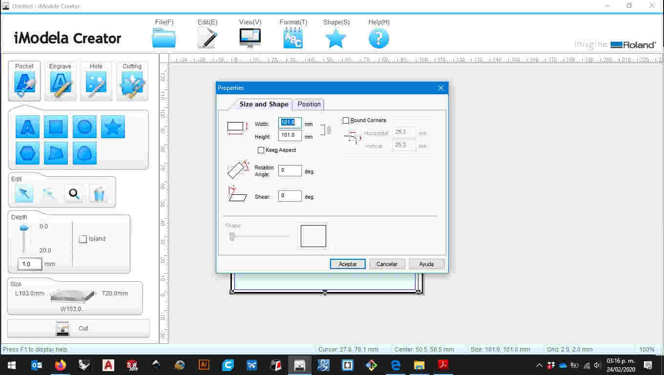
setting the geometry dimensions
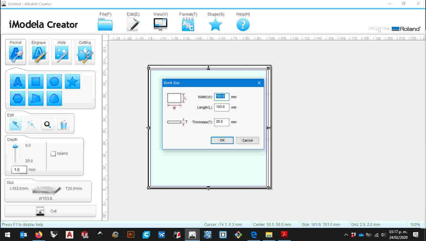
setting the dimensions on the material
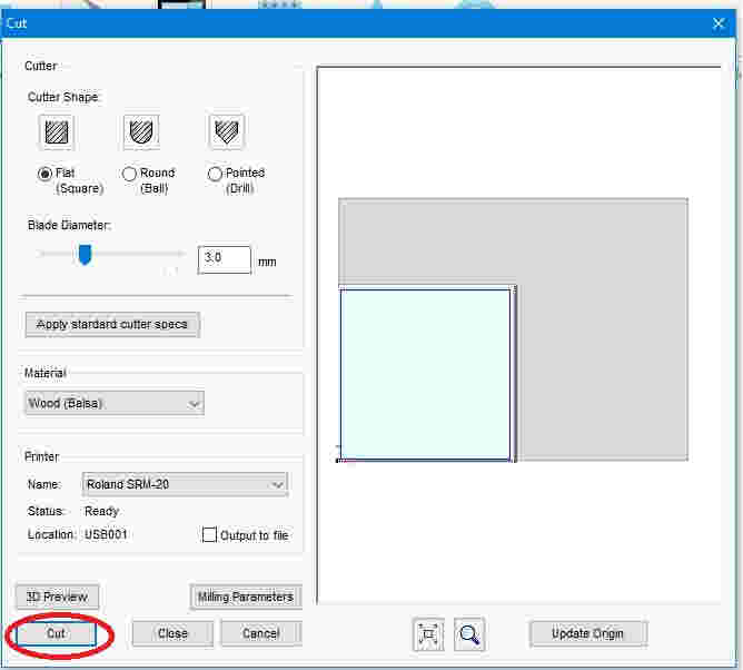
WARNING
you only should do this if you already done the origin settings before otherwise you’ll end up hurting the endmill, the machine or yourself.
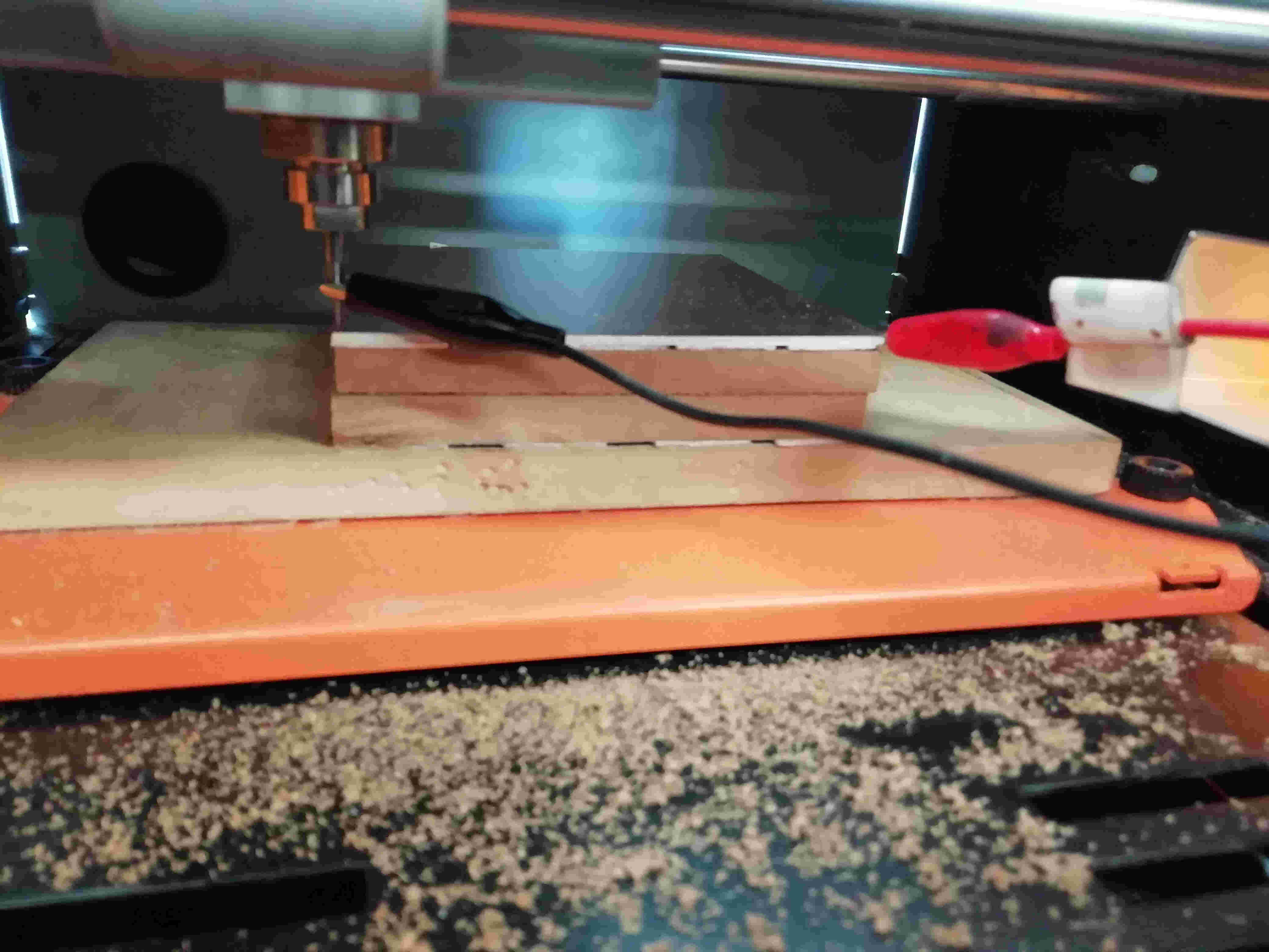
At the end of that operation you’ll end up with a completly flat Surface to work on your PCB traces and outlines.
2.3.- set your blank PCB board
now you have a flat Surface to work with, first you’ll need to clean your PCB blank board with some IPA (isopropil alcohol) to get rid of the dust and grease, other wise it will be harder once it is all cut out. Then place it on top of the sacrificial layer using some double sided tape in the side without copper.finally changed the cutter to a 60° “V” cutter.
2.4.-set your zeros on the PCB. (method 2)
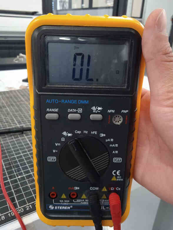
Now, the copper is a nice conductive Surface and your cutter is made of som Steel alloy although Steel is’nt a good conductive it’ll be enough for some continuity tests with a multimeter. So grab a multimeter and place it on continuity test attach the end of a double alligator clamp to the copper Surface and the other end to one of the terminal on the multimeter. Now clip the cutting tool with other alligator clamps and the attache the end of that to the other terminal on the multimeter to closet he circuit. Start jogging the Z axis until the you hear the buzzer from the multimeter sound now that’s more comfortable than the paper method and more precise but you’ll always have to remember to unclip the aligators from the copper and the cutting tool otherwise you’ll end up hurting the machine or yourself. So, click on the Z button on the right side of the VPANEL window to create a new origin for this tool.
 clamping the multimeter on the tool and the surface
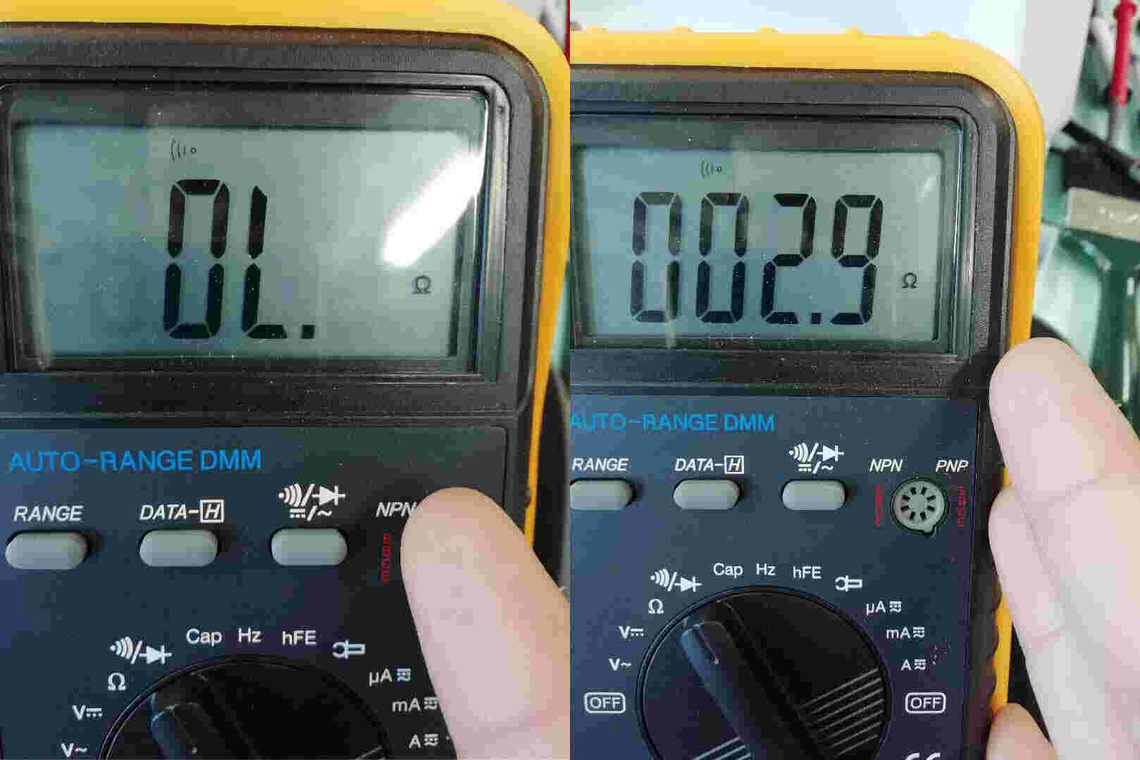 on the left the multimeter shows OL (open line), on the right it show a value of about 3 ohms it means you have touched the copper on the machine
WARNING
Make sure that your multimeter handtools and alligator clamps are outside the machine before start cuttin otherwise you’ll end up damagin something.
Now, you are ready to start cutting traces.
 Click on the “CUT” buttton on the lower right side of the VPANEL window.
 Click on “Delete all” button to erase all of the previous Works with the machine.
 Click on “add” and then select your .rml file i’ve created using Fabmodules.
And then click on “output” to start the machining.
the machine is done change the cutting tool to the 3mm endmill again and used the multmeter method to set a new Z axis origin. Then again click on cut/delete all/add/select the file /output to start cutting the outlines of the FabISP.
here is a timelapse of the flattening of the sacrificial layer
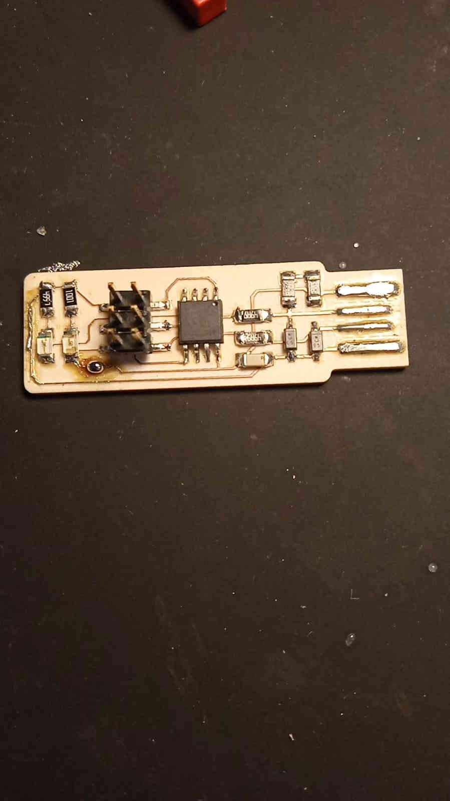
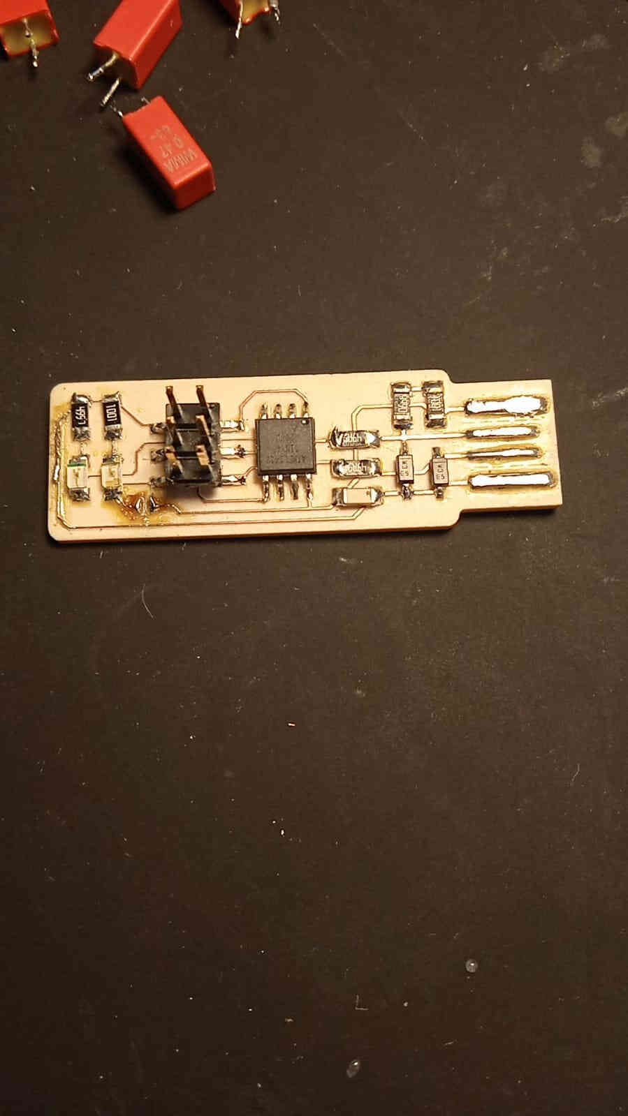
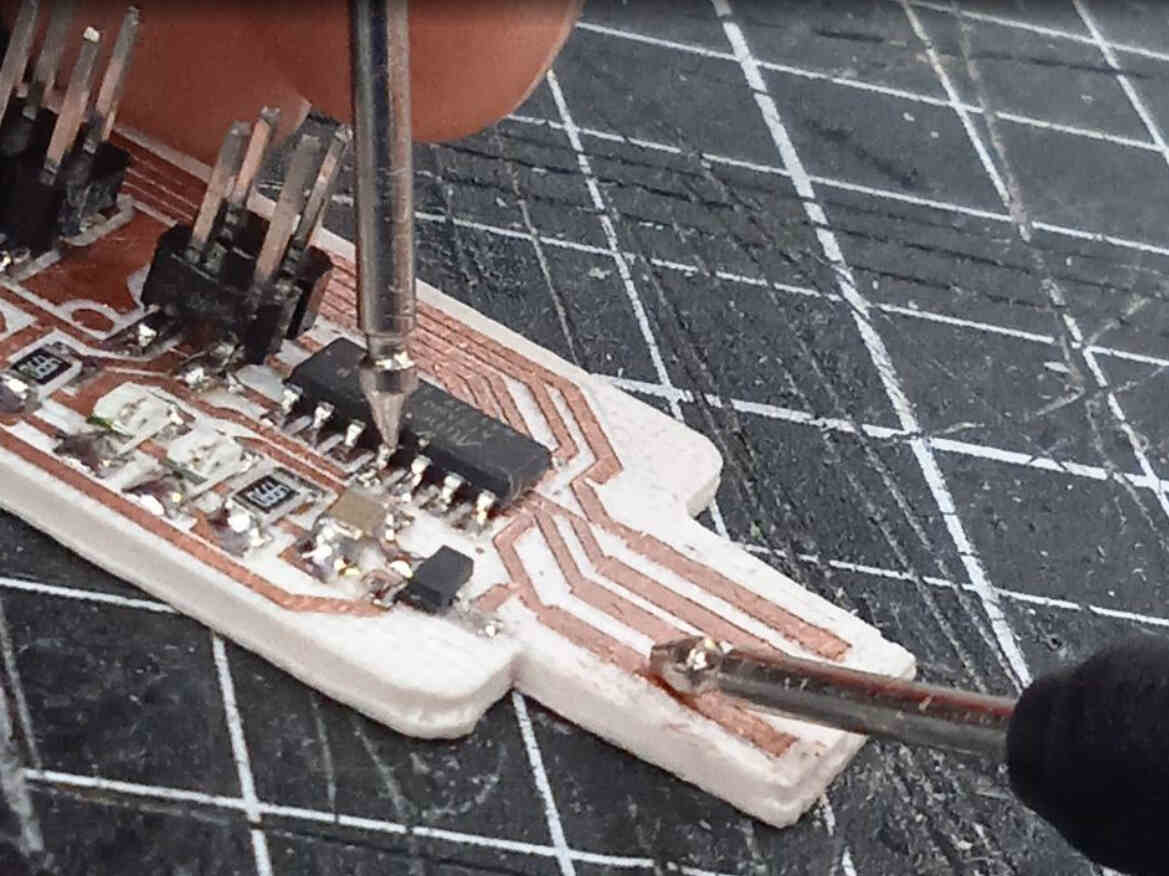
3.-solder the components on th isp
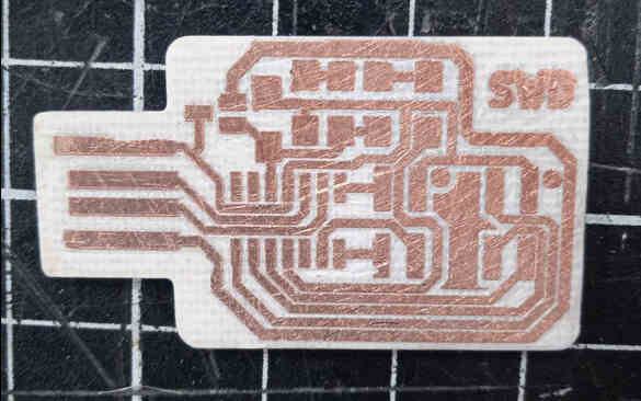
At the end of the machining process you’ll end up with something like this

at the end you will have a completly cut board just had to sand away the burs
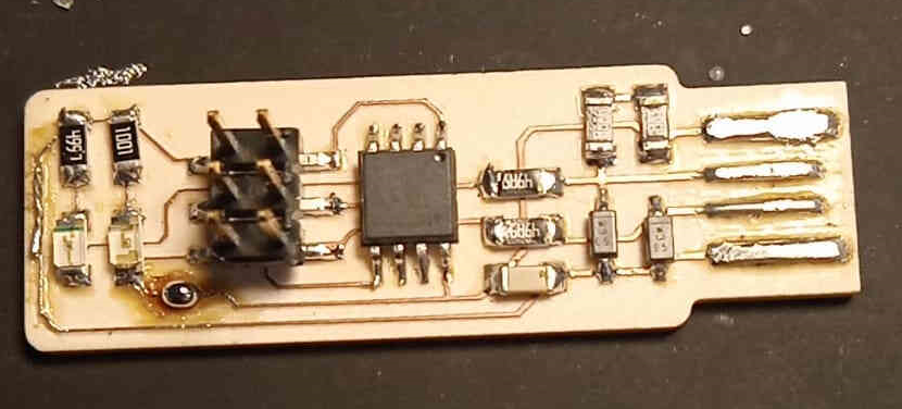
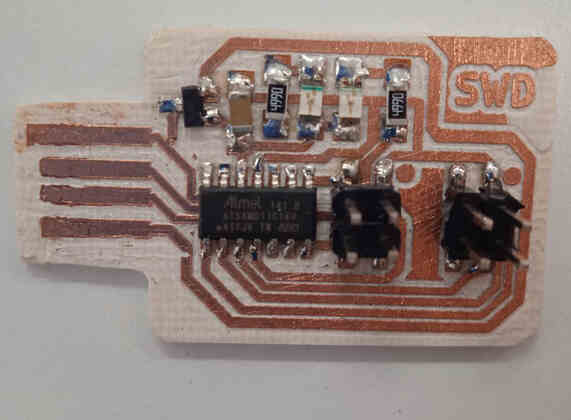
At the end of the solderin process it should look like this...
Hopefully program the fabisp.
programming de ISP
How i did it
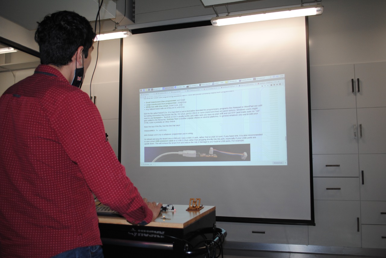
After all of my struggle to make my ISP on windows my friend Jonathan had the brilliant idea to use the raspberry PI we had laying arround in the lab.
I launched tha raspberry and hook the HDMI from the raspberry to a Projector.
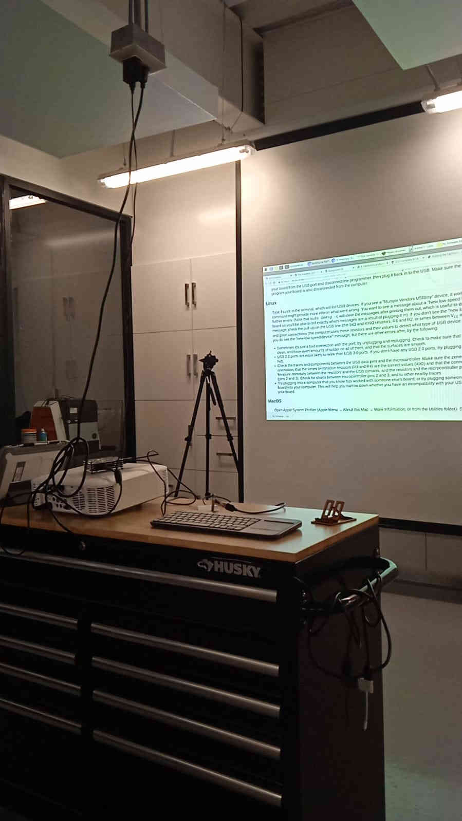
The raspberry PI conected to the projector
From there i launched the chromium browser and opened the brian's tutorial on how get running the Attinny45 based ISP he designed.
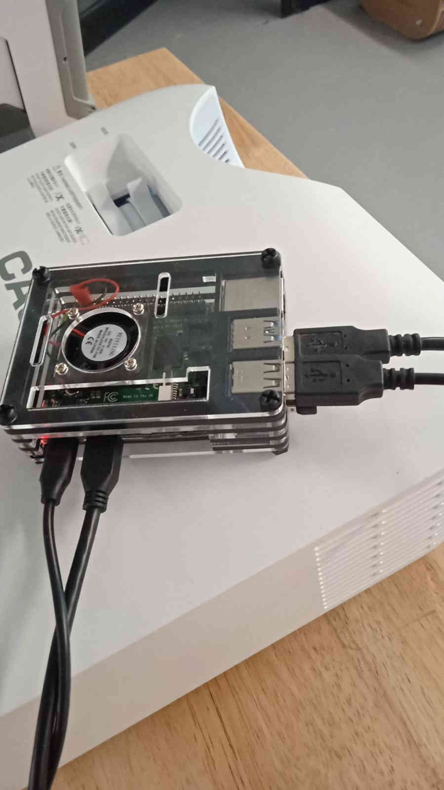
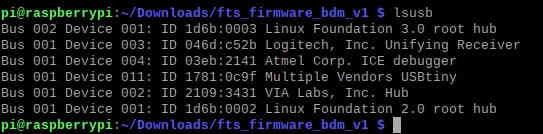
Since we have in our lab the Atmel-ice programmer. That's what i used to get it running.
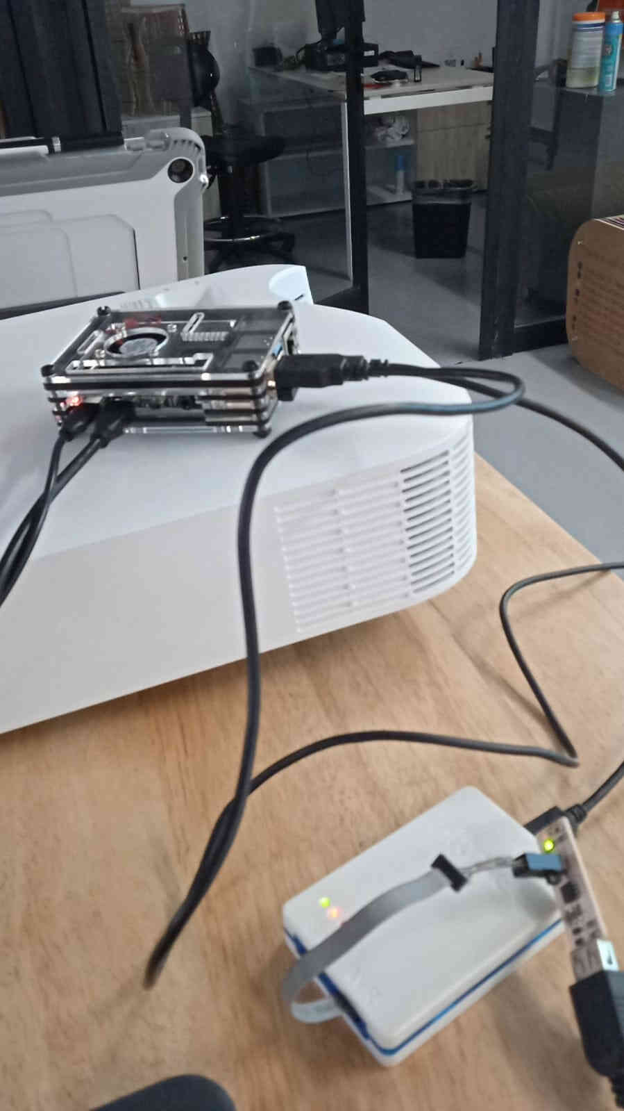
The atmel ice already hooked up to the raspberry
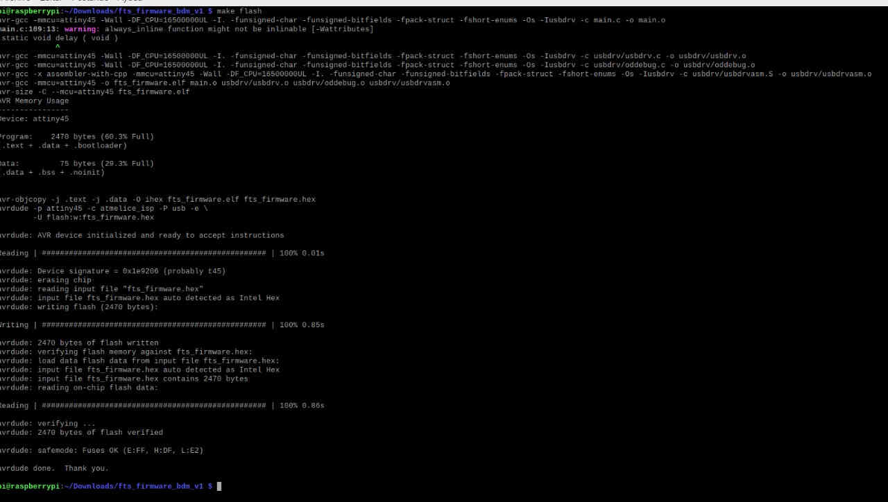
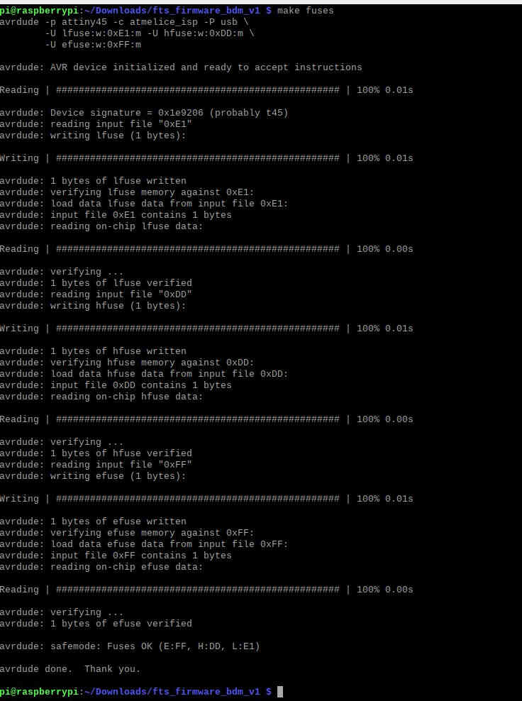
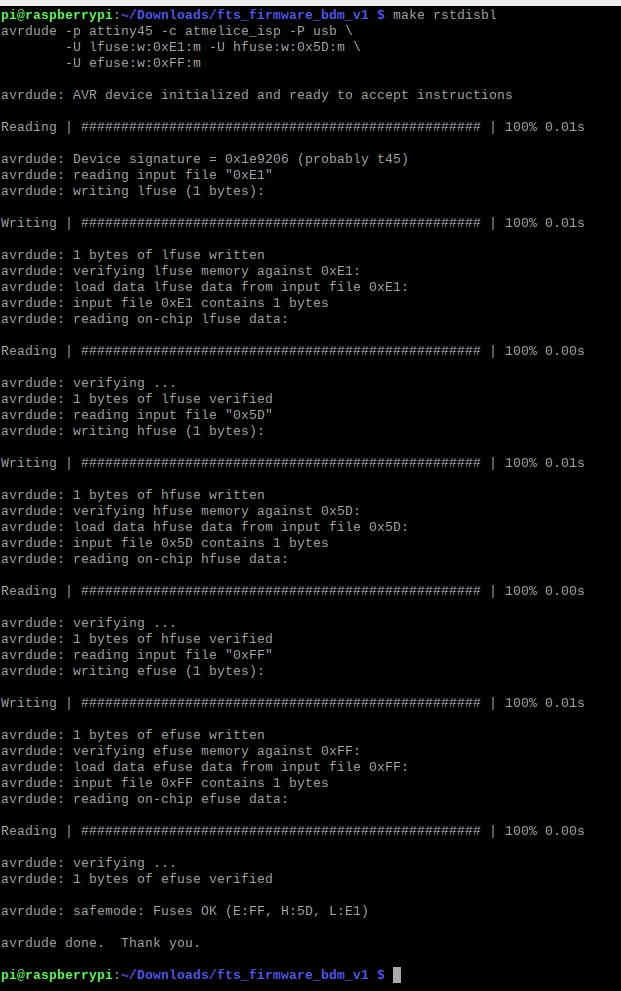
The first was to download to the raspberry the firmware available on brian's page.
and on line #19 (wich is highlighted on the screenshot) i replaced "usbtiny" with "atmelice_isp".
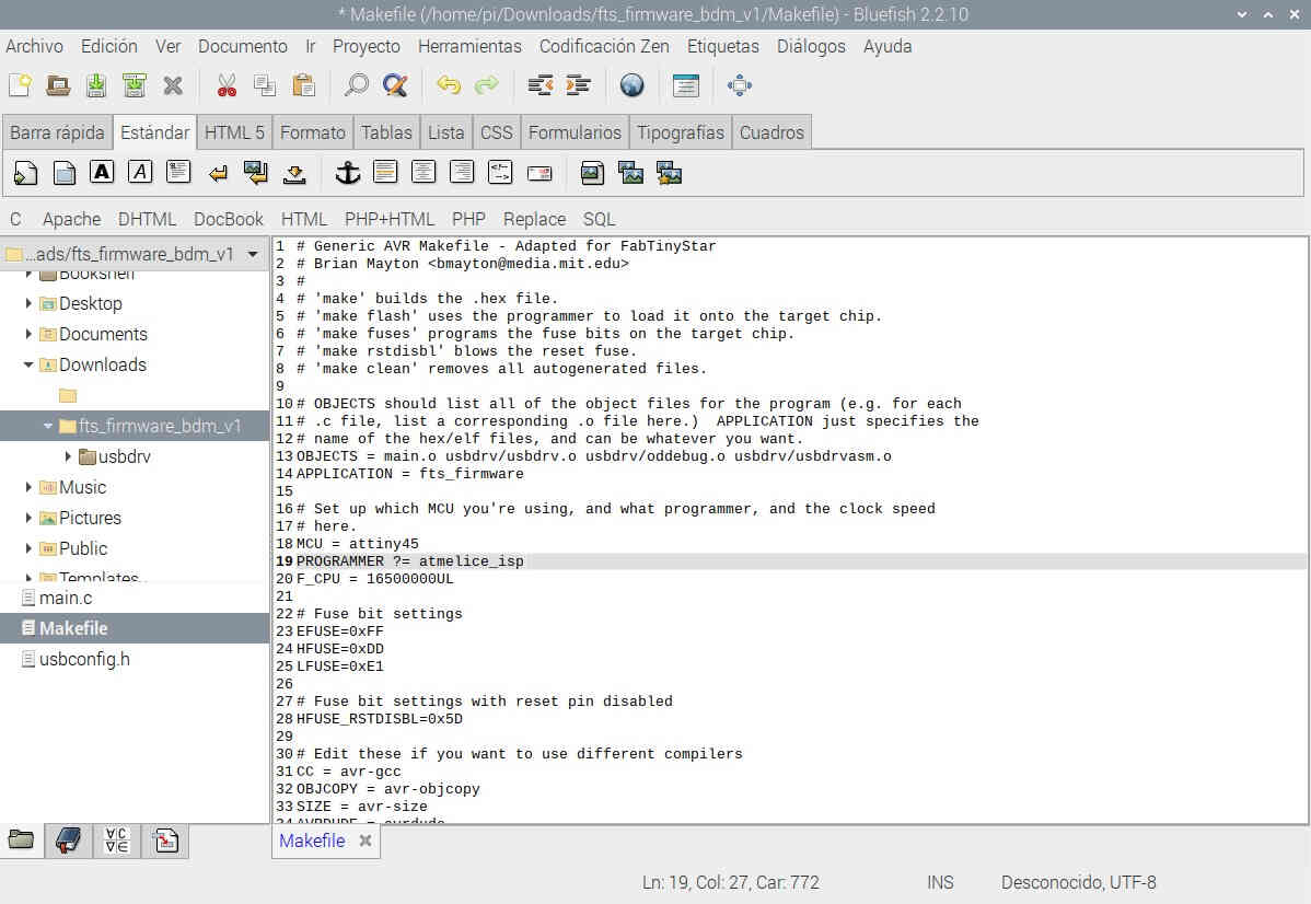 Bluefish screenshot of the "Makefile"
Then i had to open the Command Terminal wich is handly visible on the desktop.
Then as brian states in his tutorial, i typed the following command on terminal.
$ sudo apt install avrdude gcc-avr avr-libc make
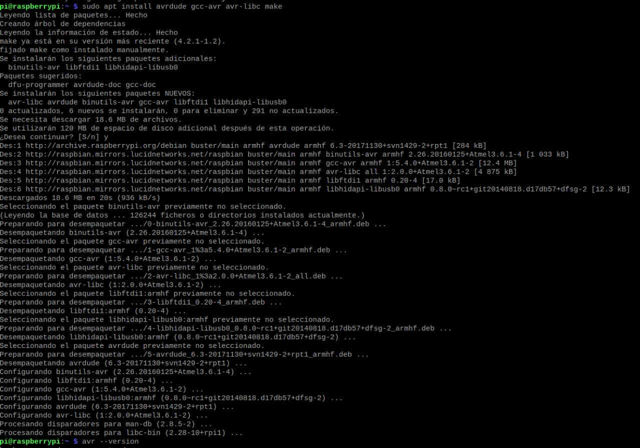 The installations command
this instrucction set the installations for avrdude, gcc-avr, avr-libc and make programs.
The sanity checks
it is for checking if the programs are correctly installed.
$ make -v
$ avrdude
and you should see something like this
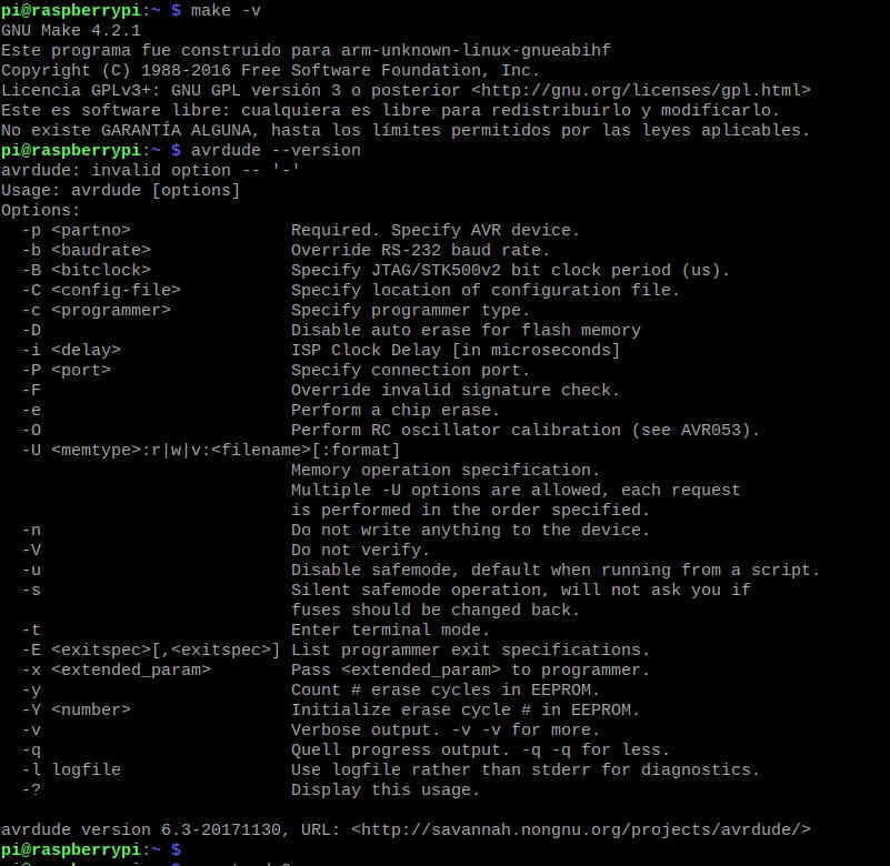 Sanity check 1
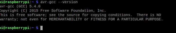 sanity check 2
The real deal
 Actual board
The USB from the target board to the USB extension cord that was conected to the Raspberry
The conections betwwen the raspberry, the programmer and the target board.
Then i runned on terminal the folowing commands and gave the respective screenshots.
Yet another sanity check
if not also gives a little troubleshoot list.
without solder jumper on the reset
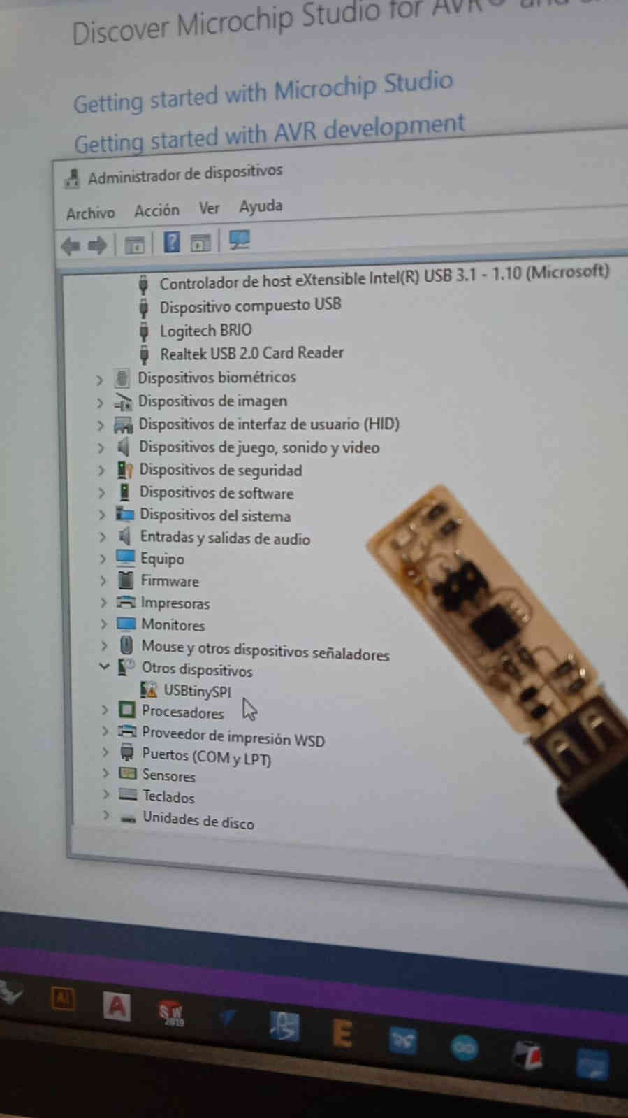
before i actually attemp to program something with it i should install the right drivers.
Also on brian's tutorial but on How to set the avr toolChain on windows he talks about a little software called "zading" wich is a driver installer tool and it's really simple to use.
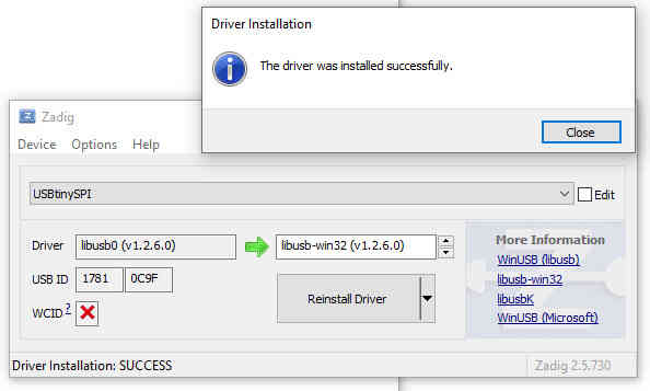
zading installed the driver for the ISPtinny for me.
with out this step is imposible to upload any sketch on any board.
The ISP driver correctly installed using ZADING shoul look like this.
Programming Quentin's programmer
In here i'll leave the programming captures from 2022 and the steps required
Disclaimer
I use a Windows 10 based system the (flashing commands and general workflow of installation may vary for another OS)
- Download the png's from the fabcloud programmers repo.
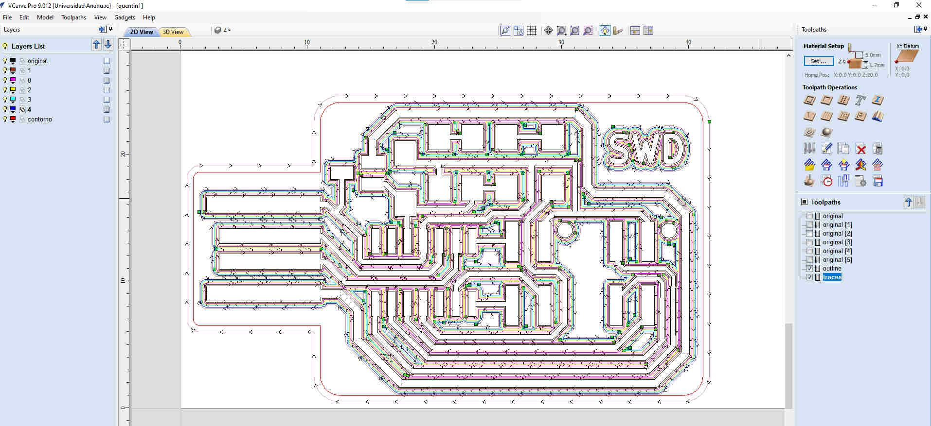
- Process them either on mods or using Vcarve (I used vcarve as usual).
- Get the rml files from your postprocessor.
- Weed the excess of copper out of the board if needed.
- Get that clean board stuffed.
- Test it with a multimeter.
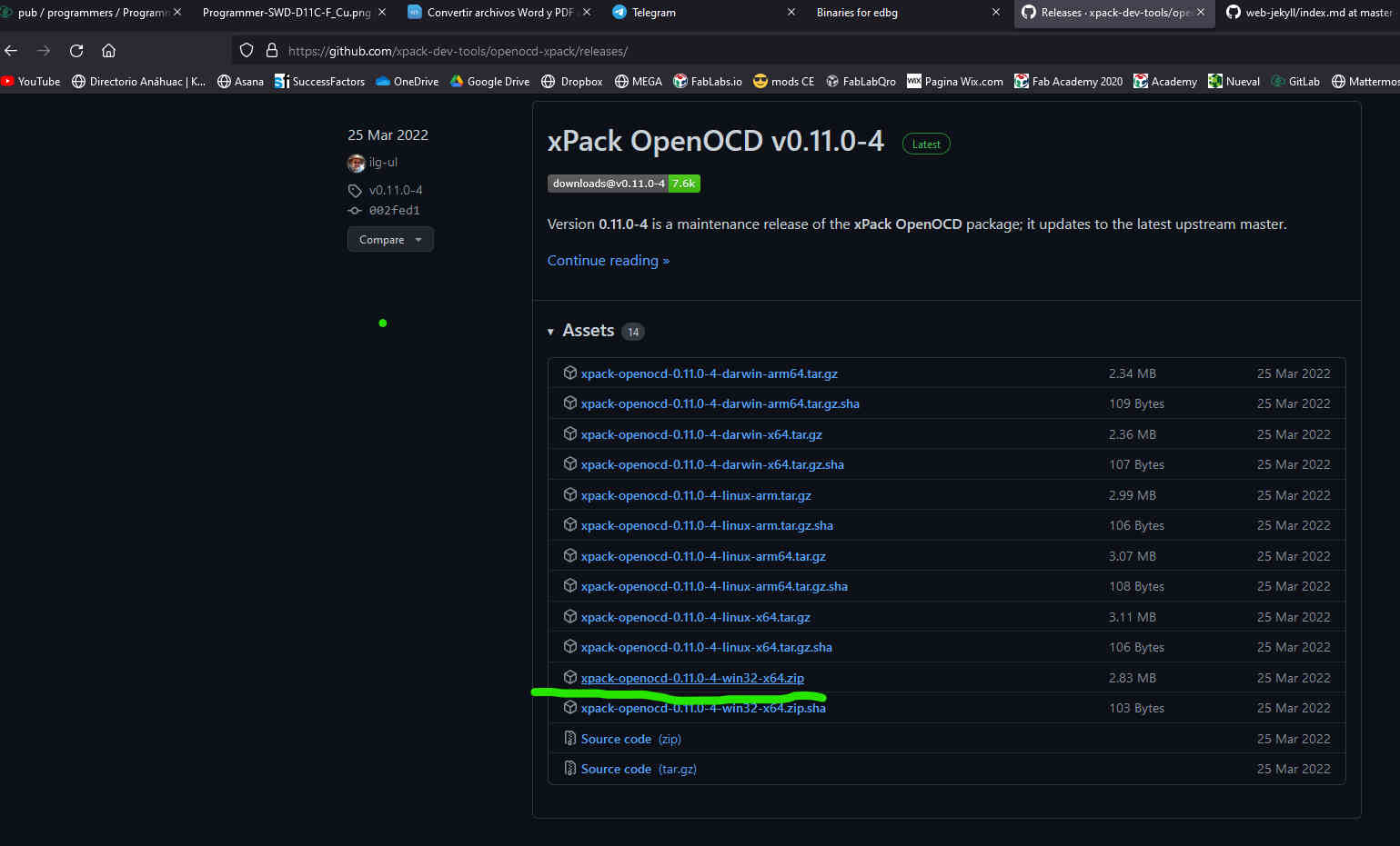
- Download an EDBG build for your operative system
- Download an openOCD build for your system.
- Download the Binary file for the programmer
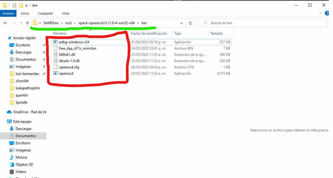
- stuff everithing in the uncompressed openocd file under bin
- Wire
- Flash the board
- Test if it worked using EDBG
- Enjoy that sweet brand new programmer.
on the web browser just right click save image as...
if need help using vcarve you can follow the steps i said on brian's ISP
HERE you can download my vcarve pro 9.0 file
HERE you can download my Roland SRM-20 rml files
i ussually used 5-6 perimeters just to save time
the rest if needed is manually peeled with the help of a box cutter or a precision knife
In my case i went into this pageit is jus a repo for the EDBG software
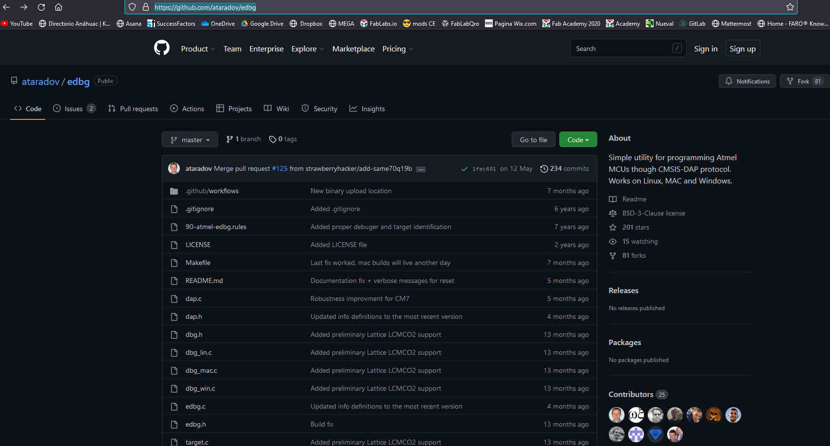 ataradov Repo
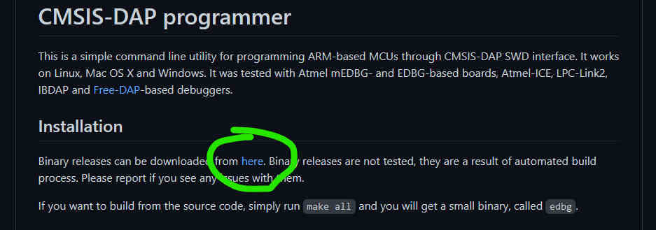
under installation there's a link
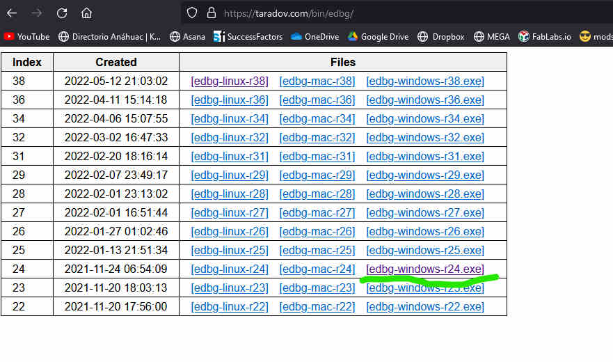
that taked me to the prebuild files for windows
HERE For windows users you also want to use a prebuild instalation file
in my case i used the link for the zip file
HERE you can download the binary file for the SAMD11C
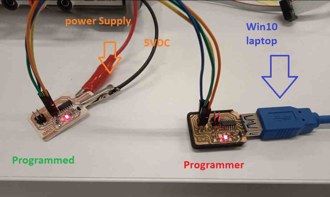
For this i needed and usb extension, an external power supply a programmer and some jumper wires
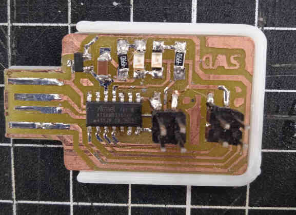
this is mexico's programmer used to program queretaro's boards
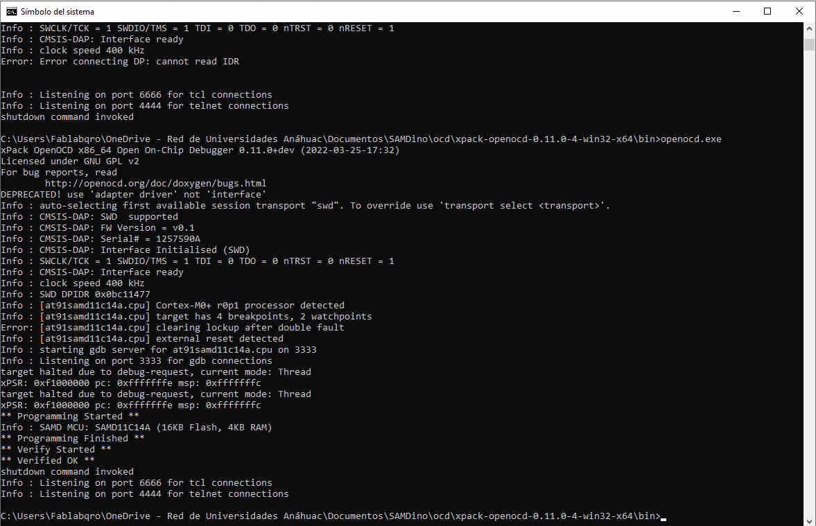
$ cd C:\Users\Fablabqro\OneDrive - Red de Universidades Anáhuac\Documentos\SAMDino\ocd\xpack-openocd-0.11.0-4-win32-x64\bin
now just plug the new board on the usb extension
back in the laptop type the following command on yellow
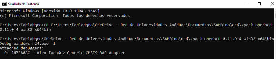
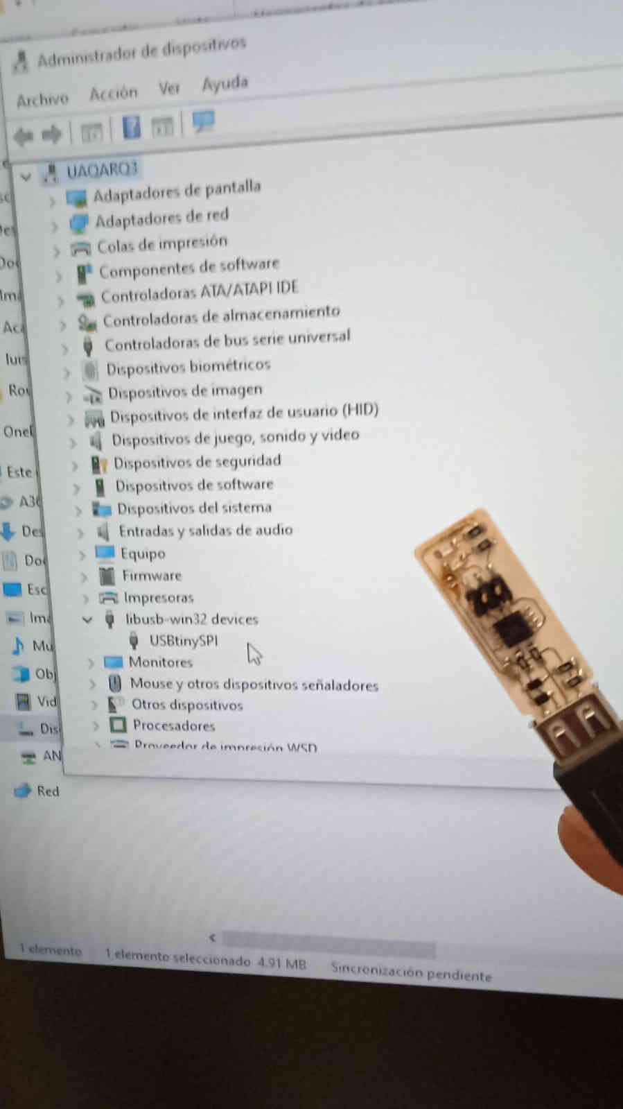
this will list the programmers conected to the laptop and if it shows the Alex Taradov Generic CMSIS-DAP adapter label you're good to go
Conclusion
Links and references
HERE Brian's original version of the FABtin45
HERE You can download brian's traces file
HERE You can download the outlines file from mods
HERE you can download my outline roland file.
HERE You can download brian's outline file/a>
HERE is the link to buy the 0.2mm endmill
HERE is the link to buy the 1mm endmill
HERE If you wish to install the vcarvepro software for yourself.
HERE you can download the Vcarve generated roland files
HERE You can download the vcarve editable file.