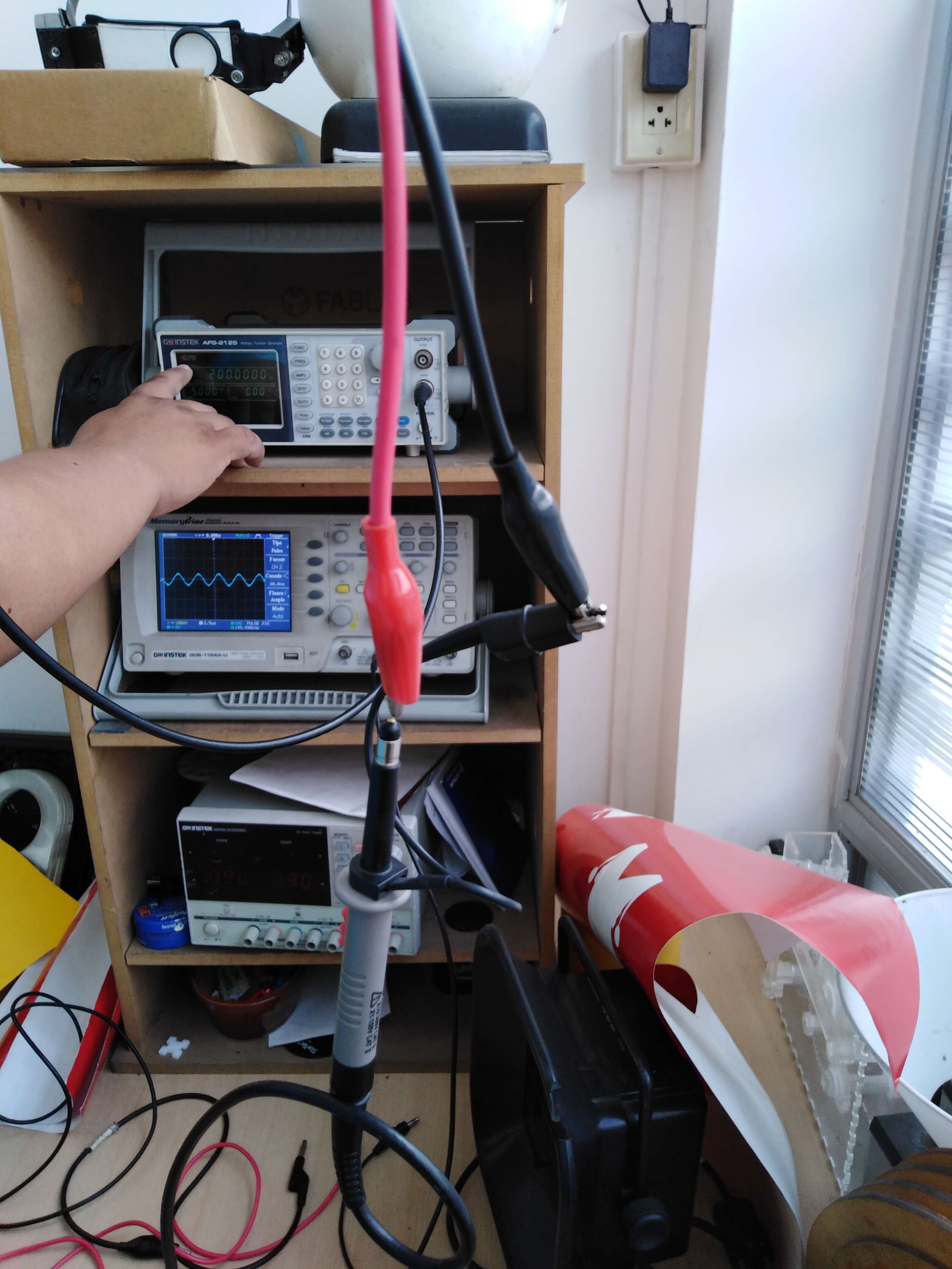
Test equipment
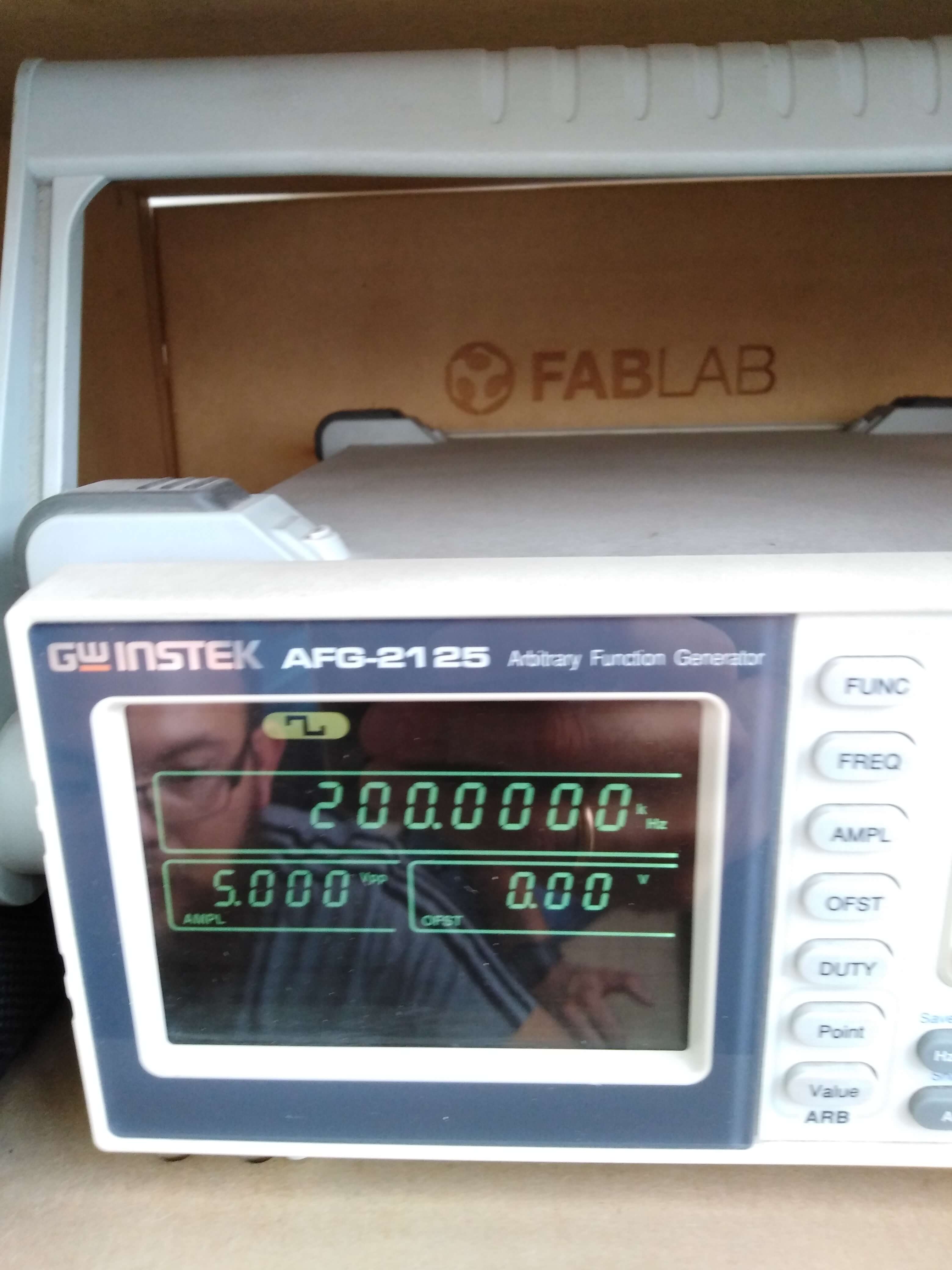
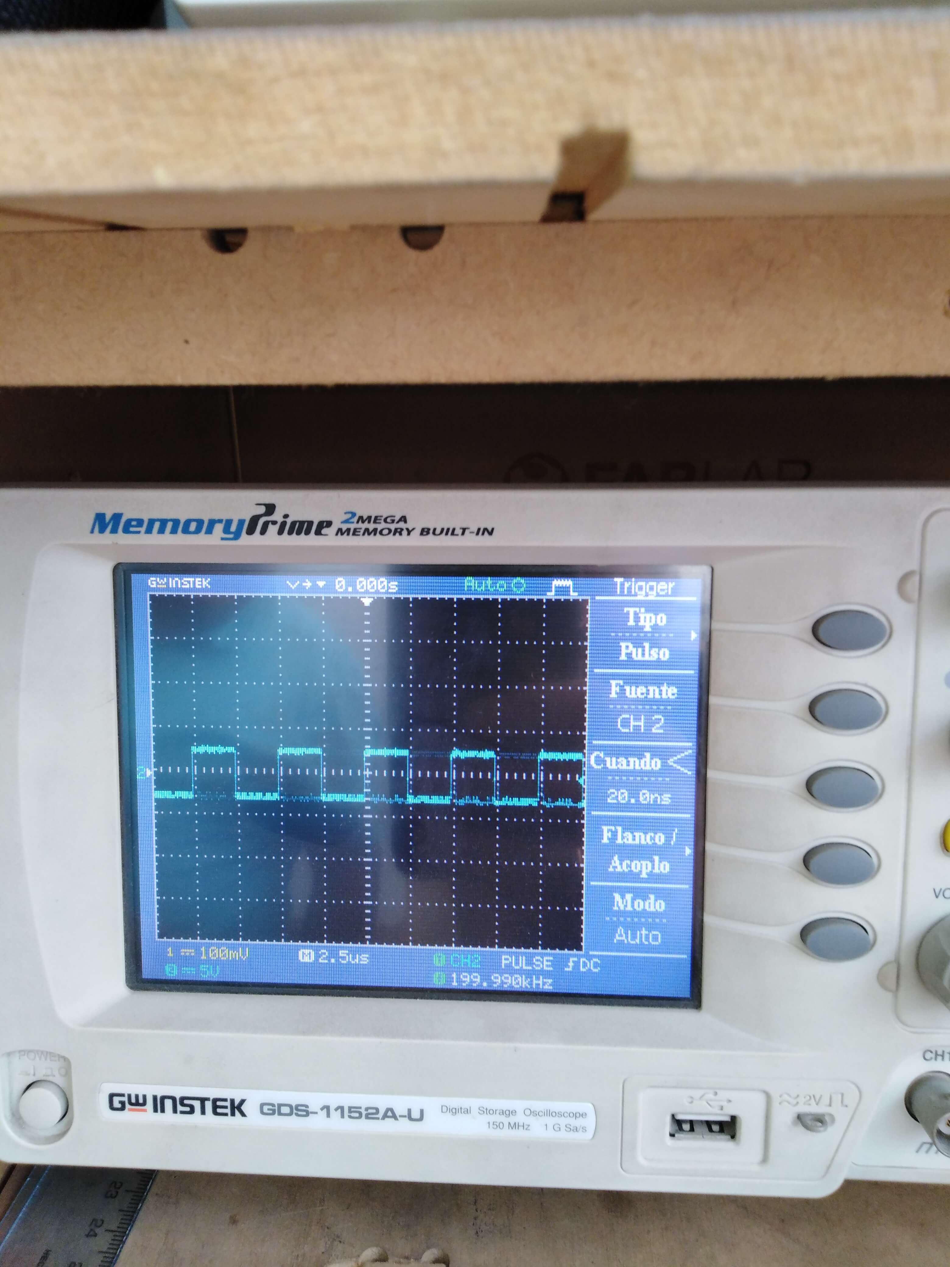
In the group assignment for this week, we use three equipment, a multimeter, an arbitrary function generator, and a oscilloscope. We learn about the fact that any electronic device has his own characteristic electric signal, so we use the oscilloscope for test if the electric signal is ok or not, that is, if we observe a deviation from the typical wave (graph the peak to peak voltage vs time) that the device should have.
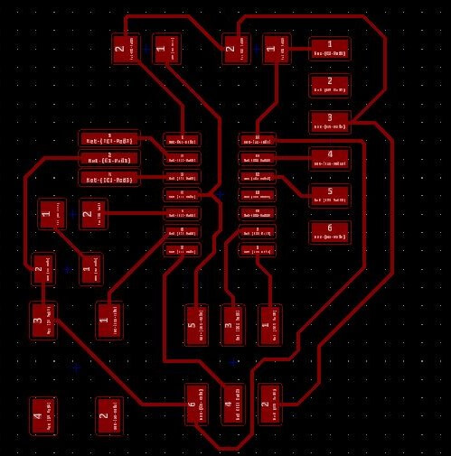
Redraw the echo hello-world board
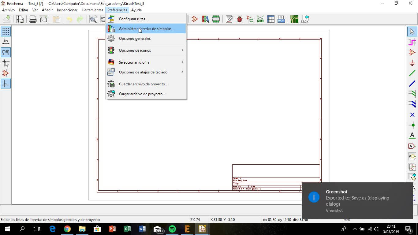
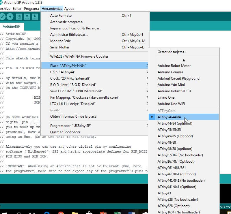
I use KiCad for this part. First of all, I reviewed the current week schedule looking for the electronic components required to build the board and found this helpful page, and use it through all the process as a guide. I observed the schematics and the PCB too. The other useful tool was the demo video of KiCad, is simple and clear. For load the libraries I have to looking for some extra info.
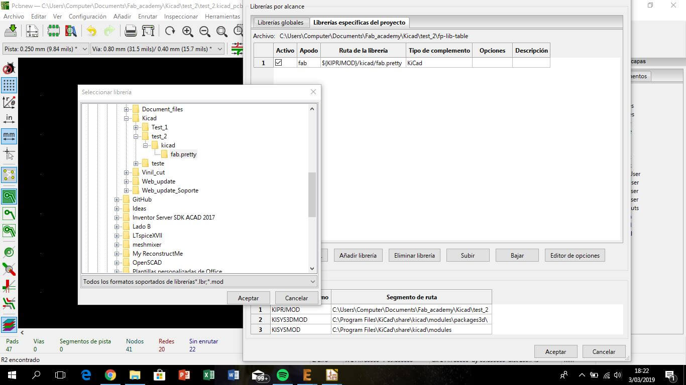
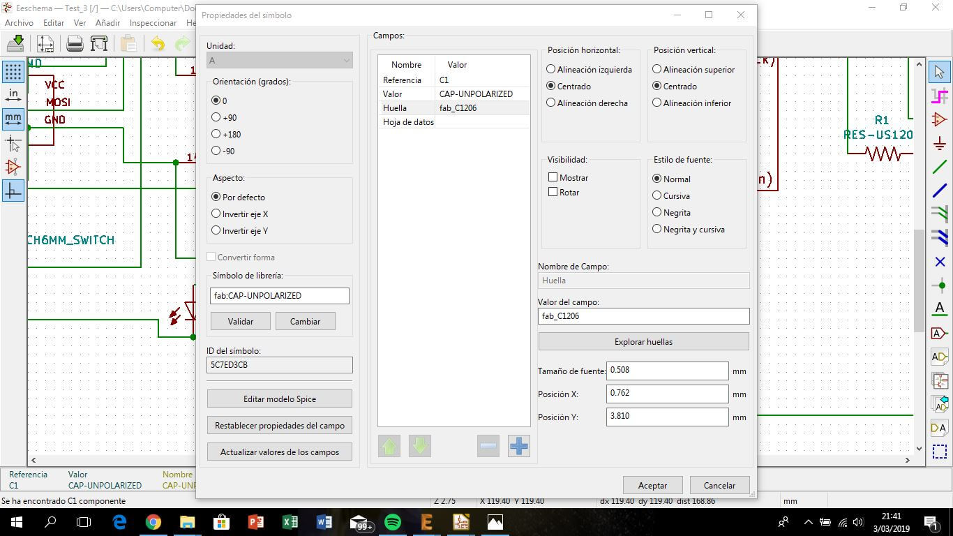
So, first of all, it is important to understand that they have two different libraries, one is for the schemas (.lib) and you will find the symbols of the components and the other for the footprints (fab.pretty file) and they are loaded separately (for download the libraries look the week schedule).
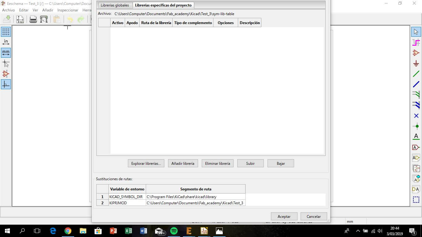
I create a new project and put the libraries file inside the project file (contents both, schematics and footprints). For load, the schematic libraries, in the schematic windows go to preferences > manage symbols library. For the footprints library is a similar process.
Load schematic library
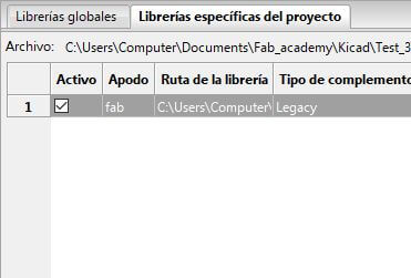
Load footprint library
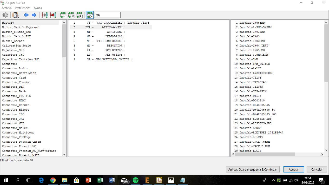
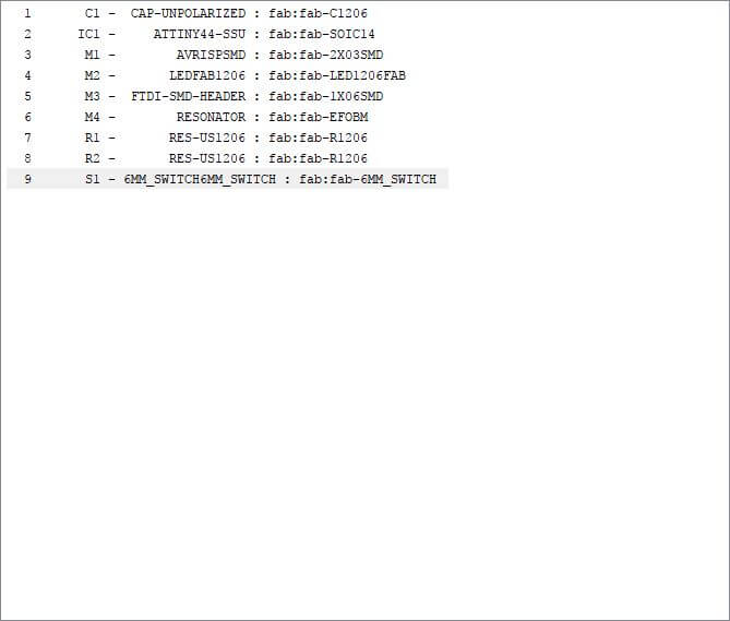
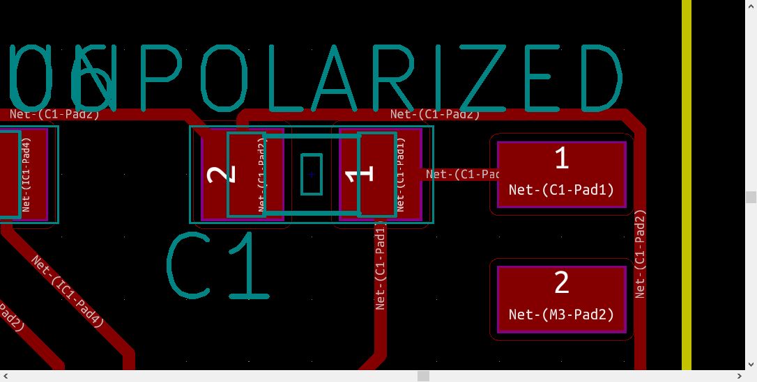
Then when the both libraries was loaded, i start to load the componets schematic view (extrac from the fab librarie) and joint them. Then I manually assigned the traces to their corresponding symbols. It is possible to filter the fab library to streamline the process. You can see the traces corresponding to each symbol in the property (right click on the symbol).
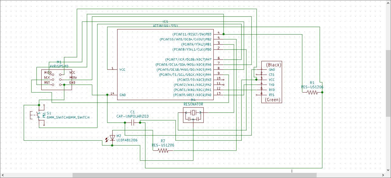
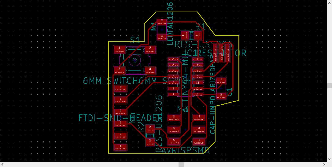
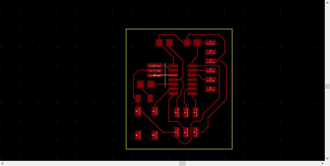
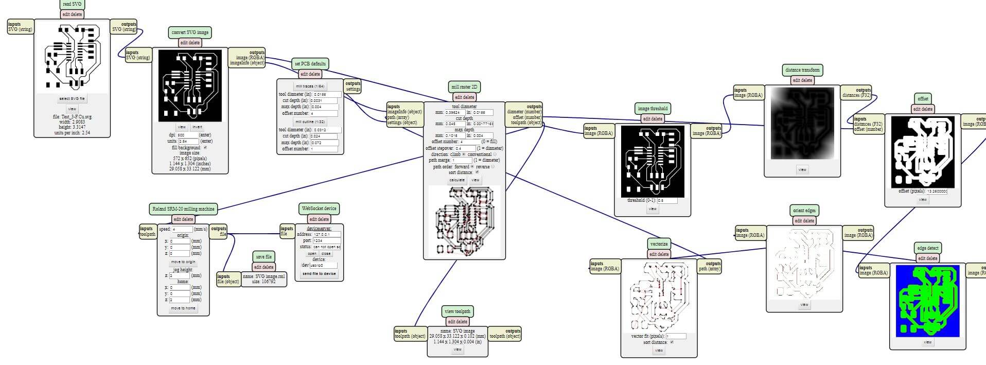
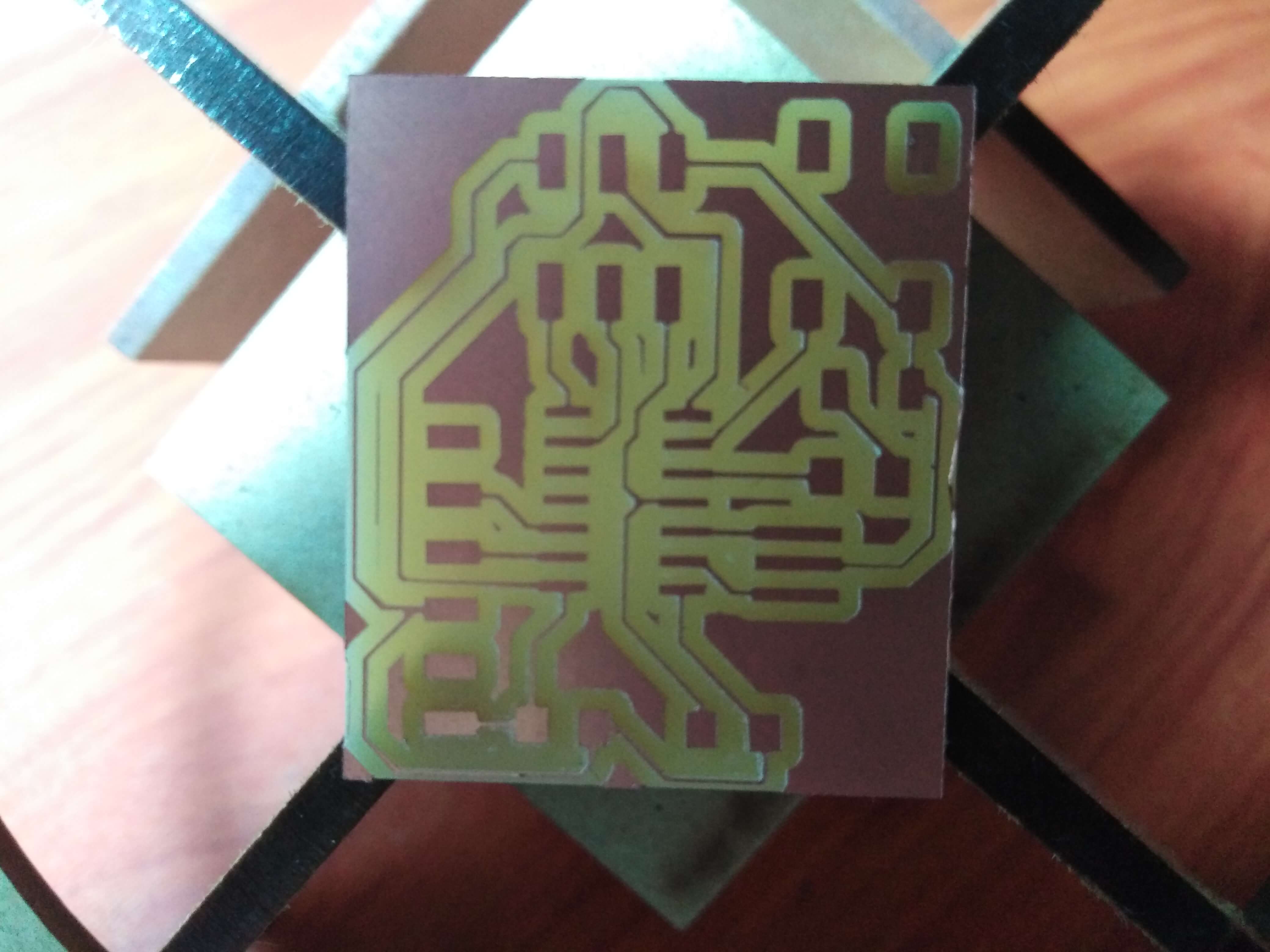
Then I generated the network and went to the PCB view. Then in the PCB view, in my first attempt the prints were very close to the terminals and this could have caused to lose the roads due to the width of the end mill, so I redraw the tracks looking for a wider space between them. Finally, I started to export in .SVG format and I passed the file (of traces and contour) in fab modules to generate the final file ready for milling.
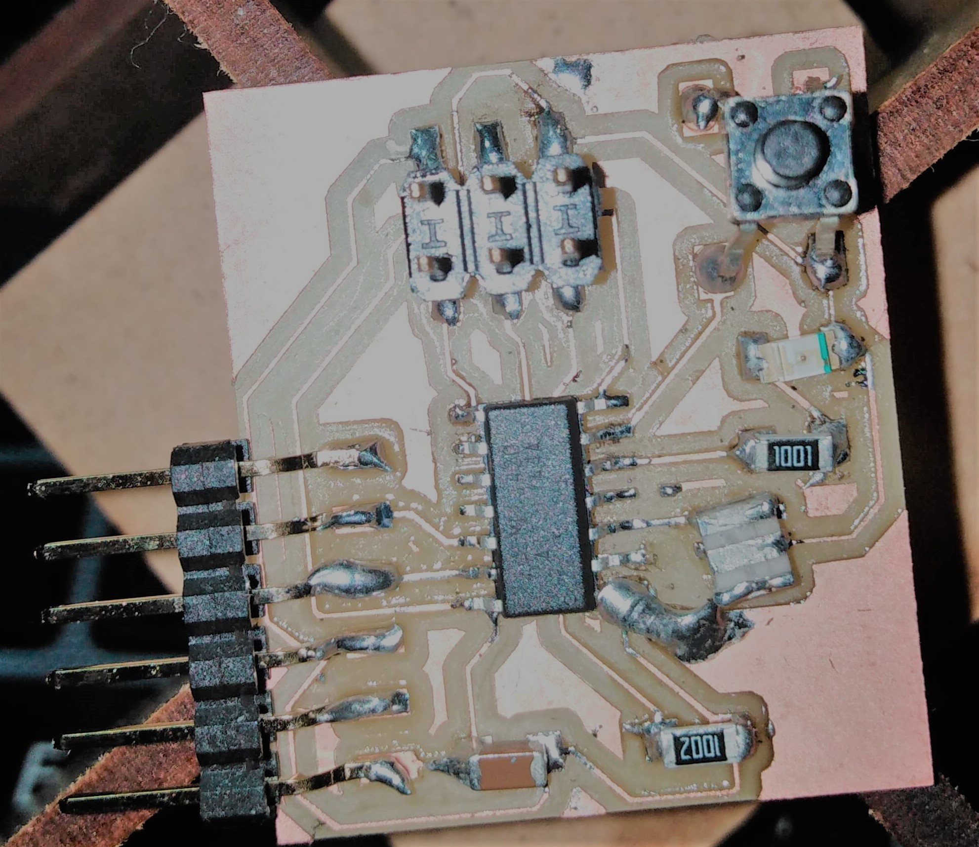
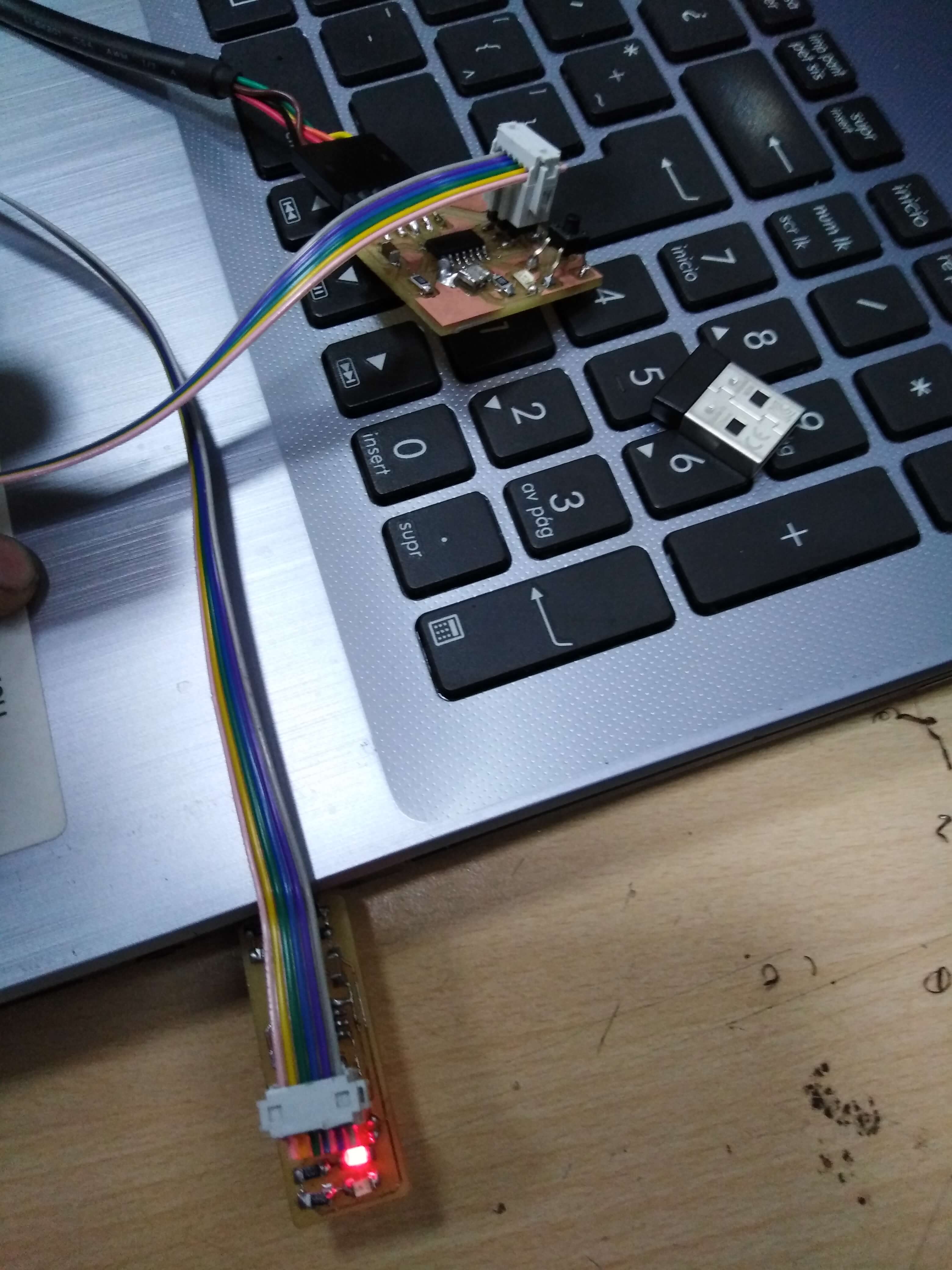
When i was traying to get out the resonator, because a bad soldering, i broke a footprint (get out from the bakelite) so I had to improvise a tin bridge.
Finally, for test, I try using arduino (reference), but after several I could not program the device.


Asignment goals
- Use the test equipment in your lab to observe the operation of a microcontroller circuit board (Group assignment).
- Redraw the echo hello-world board, add (at least) a button and LED (with current-limiting resistor), check the design rules, make it, test it.
- Extra credit: Simulate its operation. Render it.
Download files: KiCad Schematic and PBC
Learning outcomes
- Select and use software for circuit board design.
- Demonstrate workflows used in circuit board design.
Have you?
- Shown your process using words/images/screenshots.
- Explained problems and how you fixed them, including how you worked with design rules for milling (DRC in EagleCad and KiCad).
- Included original design files (Eagle, KiCad, Inkscape, .cad - whatever).