This technique explores using a fitted 3D printed mold as a guide for laying out and trimming copper tape traces by hand to make a quick PCB-style circuit.
Introduction
My 3018 CNC machine had been giving me trouble. Auto leveling was off, and the copper boards were a little bit smaller than I needed, so I decided to explore an alternative method using a 3D printed mold.
Reflection: Choose a fun filament color that doesn't clash with your copper tape. Soldering may require some skills and experience. Use flux well for quick and clean soldering.
Research
I needed to check the 3D printed trace guides to ensure an easy making process. I looked at how copper tape behaves around corners, how much spacing is needed between traces, and how high the printed guide needs to be in order to support easy hand cutting.
Key things I tested and observed:
Compare trace heights that can be cut cleanly with a knife.
Check how strongly copper tape adheres to the 3D print.
The offset needed between the mold trace guide and the copper tape.
Review how component pads and soldered joints will connect to taped traces.
The main design constraint is balancing precision with ease of assembly. If the mold is too tight, it doesn't give enough room for the tape which can lead to tearing or misalignment, and if it is too loose, the guides can't be as effective and precise.
Height Tests
I tested different mold heights to determine the optimal guide thickness for clean copper tape cutting. Here are the height variations tested:
0.4mm Height
Observation: At 0.4mm, the guide is very subtle and minimal. This height was a little difficult to cut because it was too low to provide adequate tactile feedback with the blade.
0.6mm Height
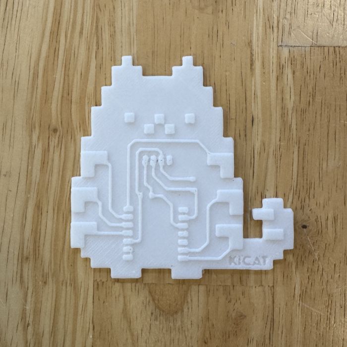
Observation: At 0.6mm, the guide provides moderate height for better handling and alignment. Copper tape adheres well and can be cut cleanly against this edge. This one proved to work well with or without the trace guide.
1.2mm Height
Observation: At 1.2mm, the guide is tall enough for strong tactile control and provides excellent cutting guidance. The increased height offers better blade support during cutting operations. However, it was too tall for some delicate maneuvers and some traces busted or broke when used with trace guides.
Conclusion: The 0.6mm trace height tested the best balance between printing efficiency and cutting guidance. Heights below 0.4mm made cutting guide not so clear, while anything over 1 mm becomes unnecessarily bulky and difficult to use with the delicate copper tape.
Design Process
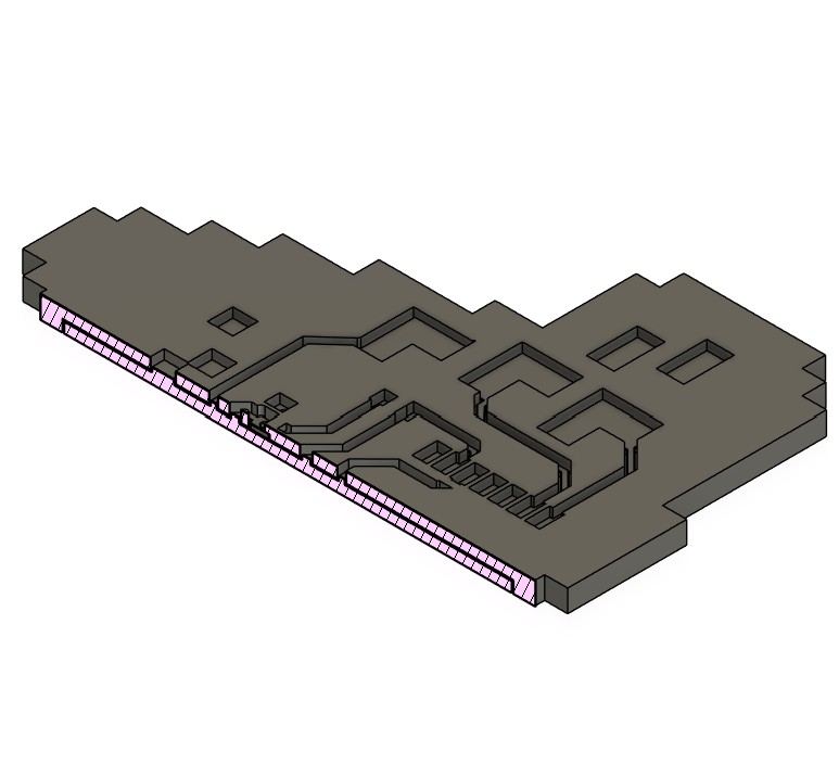
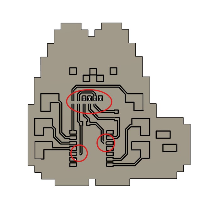
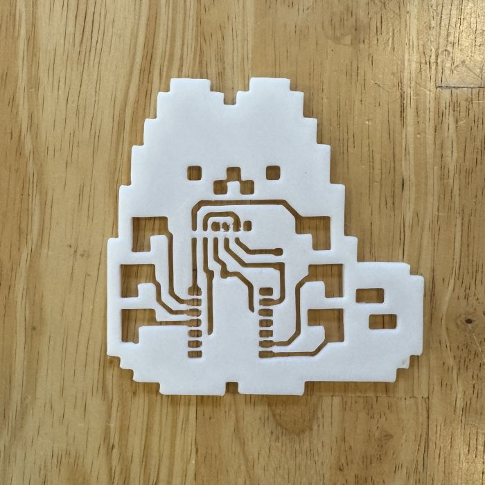
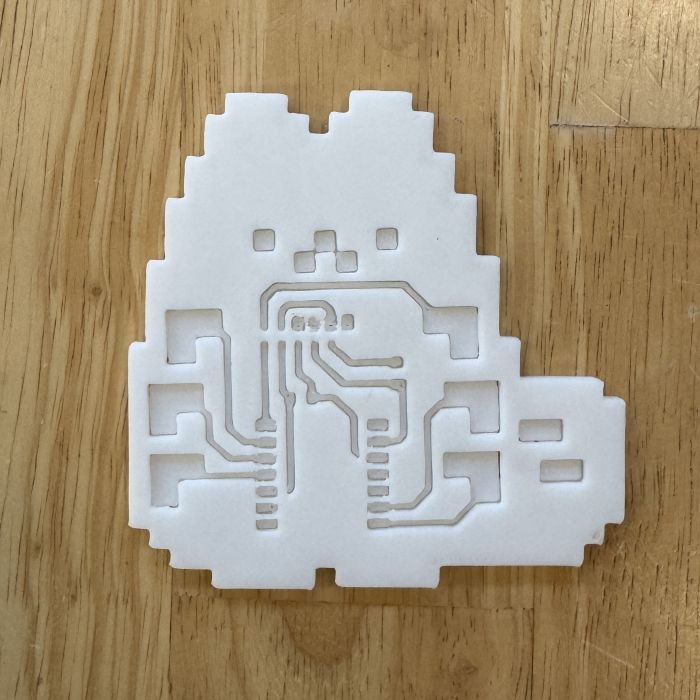
I exported my KiCAD pcb design as SVG files and had to use a 2D tool to convert them into DXF format for Fusion 360. That was an annoying extra step, I might have to try and look for a more direct workflow in the future.
I set up parameters in Fusion 360 so I could quickly change trace height and spacing during testing. I also added small bridges on the trace guide to support thin sections that were prone to bending or breaking as we can cut the parts that were skipped due to the bridge after releasing the mold.
For the offset for the trace guide I tried 0.4mm so that the blade can accurately follow the intended path, but I found out that it was not super necessary as we can just follow the edge of the guide directly. so I set the offset as 0.2mm since the copper tape is supposed to be 0.05mm thick.
Section analysis view to evaluate trace guide dimensions and alignment with mold part.Fusion 360 parameter setup used to quickly adjust key dimensions for testing.Bridge features added to support thin trace-guide segments during handling. Refined Fusion 360 guide after parameter tuning and bridge placement.
Trace width best between 0.6mm - 1 mm
Offset (gap between trace and guide) best around 0.2mm, but it depends on your 3D printer's precision and the copper tape thickness.
Generated height variants (0.4mm, 0.6mm, and 1.2mm) from the same base layout for fair comparison.
WooHoo! Designing with Fusion and Parameter setup was tested and easy for me, but I was not satisfied with the entire design to print process. I tried creating an app to make my PCB design PNG files into 3D file. It is still in early development and needs more testing, but seems to be worth a try. Link is in the sidebar.
I might also try making something for Mods
Making Process
Materials and Tools
Core items used in this technique study:
Item #
Item
Purpose
Notes
Format
Status
1
Copper tape
Conductive traces
Needs to be as big as your PCB and have a strong adhesive backing
Roll cut to correct size
Used
2
3D printed top
Trace outline guide
Sized to fit the back surface accurately and have the trace paths clean with no failed print
Printed part
Used
3
3D printed bottom
PCB substitute surface with trace
Needs to have 0.6mm trace height and at least 1.6mm thickness overall for stability
Printed part
Used
4
Precision knife
Cutting and cleanup
Important for corners and pad openings 30degree blade preferred
Hand tool
Used
5
0.8mm drill bit
Drilling holes for component pins
Used to create precise holes for through-hole components
Drill bit
Used
6
Multimeter
Continuity testing
Used to confirm traces are isolated and connected correctly
Measurement tool
Used
BOM Photo Gallery
Copper tape big enough to cover your traces3D printed top3D printed bottom0.8mm drill bit photo placeholder.
Placeholder box
Precision knife photo placeholder.
Placeholder box
Multimeter photo placeholder.
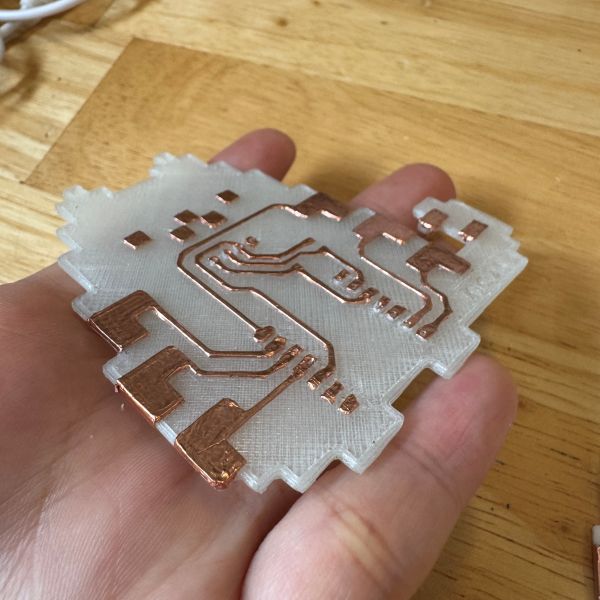
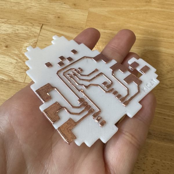
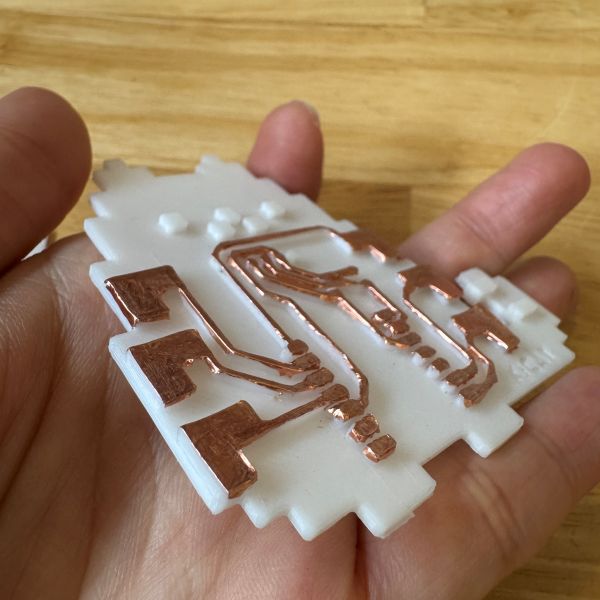
The fabrication workflow is organized around using the printed mold as the base PCB while the trace guide serves as a positioning and cutting jig.
Step by Step
01. Clean your 3D prints
The 3D prints should be cleaned so that there are no stringing or debris that could interfere with the copper tape application and adhesion. Imagine sticking protective film to your phone. :D
Check the fit of the mold and trace guide before proceeding.
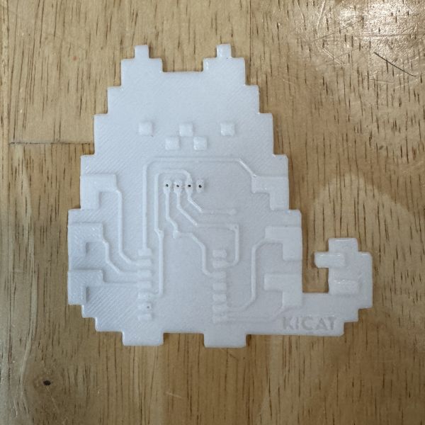
02. Drill Holes
Drill the necessary holes in the mold before applying the copper tape. Make sure to clean the 3D print again after the hole making especially the surface of the pads as they can be bumpy after drilling.
While making the holes after copper adhesion is an option, it is harder to drill on tape without damaging it.
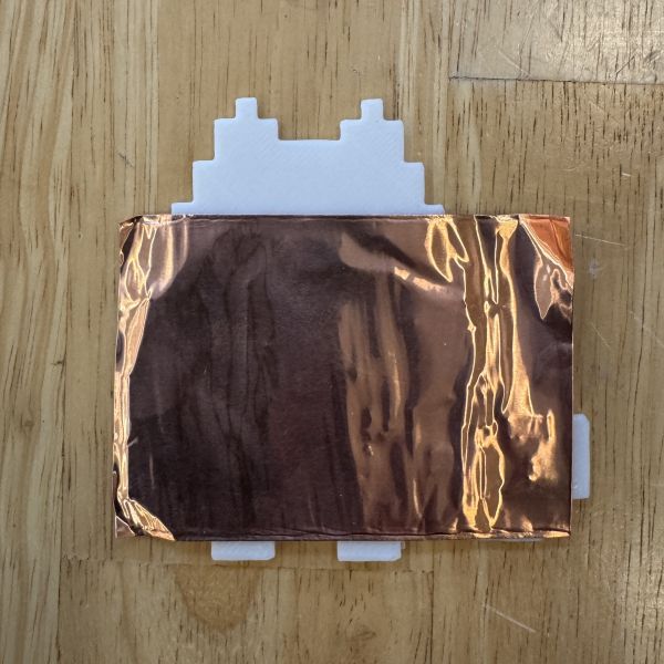
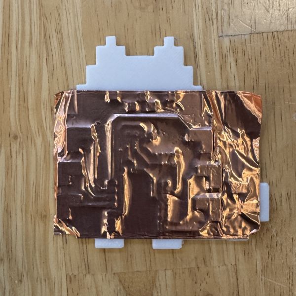
03. Apply and Trim Copper Tape
Place copper tape on the mold part to cover the intended trace paths. You don't have to try to stick down everything at this point just enough for them to be positioned correctly.
04. Wipe Down
Gently wipe down the copper tape with a little force around the traces to create a more secure adhesion and outline of the traces.
Use a lint-free cloth or just your sleeve to avoid leaving fingerprints on your beautiful copper.
05. The fit
Trim the outside edges of the copper tape to match the mold's outline, so that the mold will fit snugly with copper tape into the printed guide part
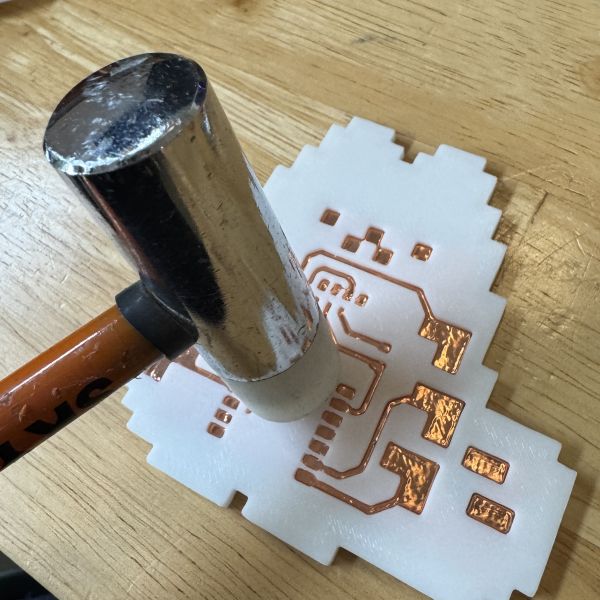
06. Hammertime
Gently tap the mold with a hammer or mallet to ensure the copper molds around the traces. You could use a needle or an awl or even a precision knife to trace around the traces for cut with the guide.
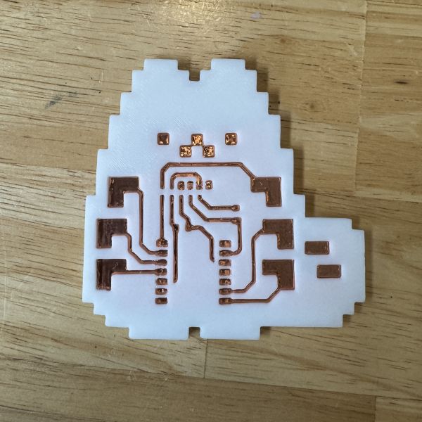
07. Trace check
Take the mold out of the guide and inspect the traces for any gaps or misalignments.
This is a good time to use a hard flat surface to rub down the pads to ensure proper adhesion and poke around hard corners and edges to ensure all parts of the traces are properly adhered.
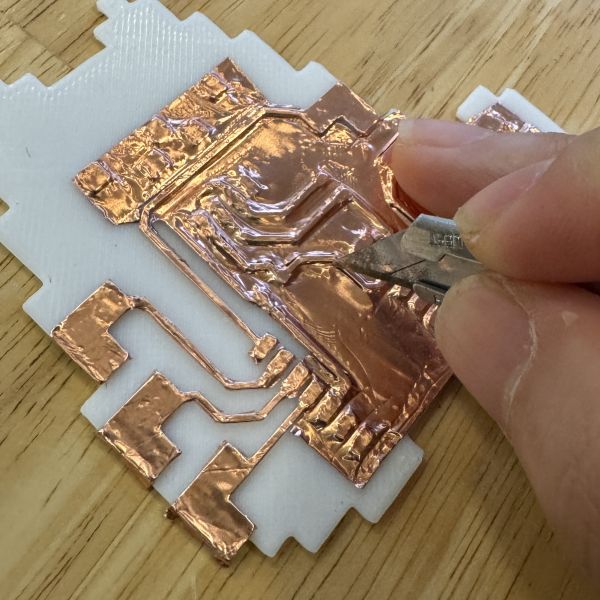
08. Cutting and weeding
Use a precision knife to cut along the edges, following the outline of the traces carefully. Use your nailes or plastic objects to hold down the pad copper when cutting between pads.
DO NOT BE CAVALIER ABOUT THIS
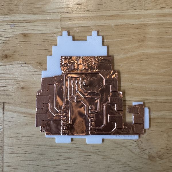
09. Finishing
Clean up and remove all of the unnecessary copper pieces and debris from the board.
If you are not confident about your skills, use a multimeter to check the connectivity of your traces.
Get a needle and poke the holes on the copper pads.
Reflection: The advantage of this approach is that the Trace guide can be reused for multiple iterations, and the mold part will be directly used as the PCB.
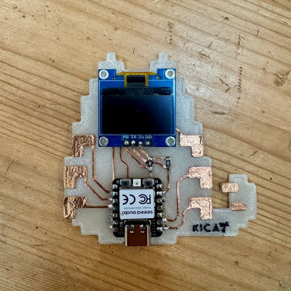
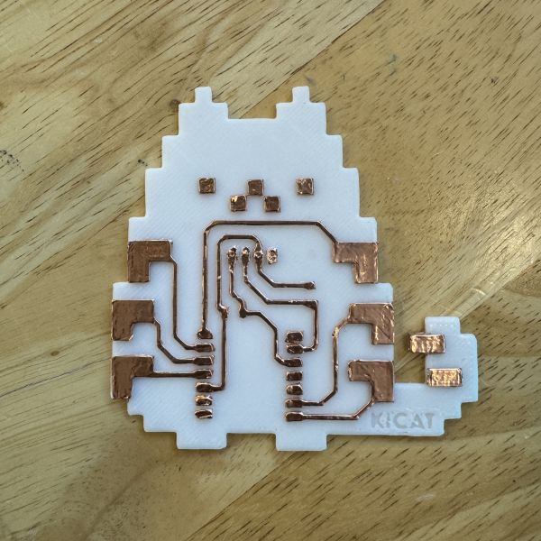
Final Outcome
The outcome of this technique is a reusable method for creating PCB-like copper trace layouts without relying on a milling machine or chemical etching workflow. The printed mold acts as a physical cutting guide as well as a sturdy reliable PCB, and the tracing guide can be reused for multiple iterations which negates the need for repeated setup and alignment.
The process is useful for quick experiments and relatively simple circuits.
Trace accuracy depends heavily on the fit of the printed guide and the cutting method.
Sharp corners and narrow spacing need extra cleanup to avoid shorts.
Reflection: I think this method can be beneficial for rapid prototyping and educational purposes to older students. Labs that may have trouble accessing traditional PCB fabrication machine, tools, and materials will benefit from this method also.
Table of Contents
Quick Info
Category: Electronics Production
Tools: Fusion360, 3D printer, knife, soft mallet, multimeter
Materials: Copper tape, printed mold and backing board