Electronic designs
Assignments for Week 7 (02.27 ~ 03.05)
◾ Group Project
Use the test equipment in your lab to observe the operation of a microcontroller circuit board
◾ Individual Project
1) Redraw the echo hello-world board
2) Add (at least) a button and LED (with current-limiting resistor)
3) Check the design rules, make it, and test it
◾ Extra Credit
Simulate its operation
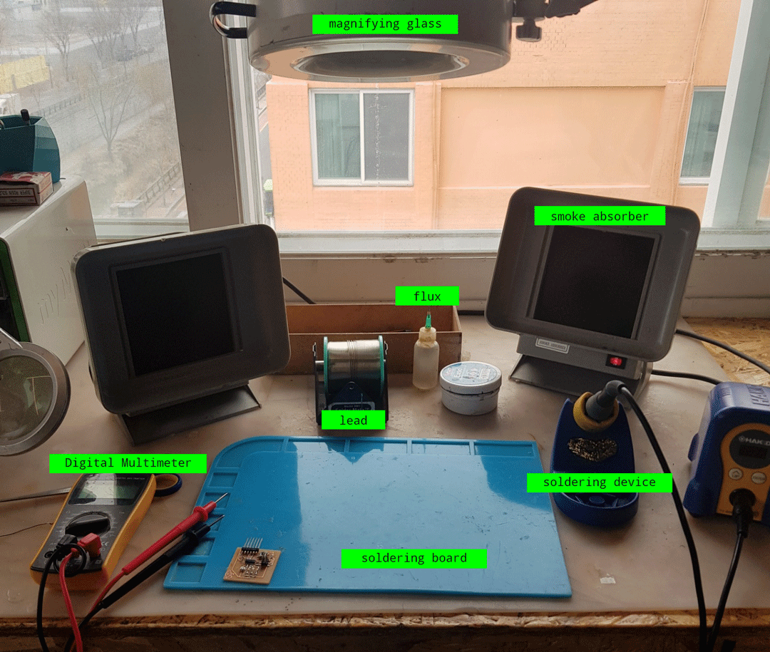
List of Machine, Materials, and SWs that I mainly used for this week's assignments
◾ Autodesk Eagle : An easy-to-use schematic editor
◾ fabmodules : Configure, Simulate milling and save the schematic file as rml
◾ Arduino
: A software to write code and upload it to the board◾ Roland SDM-40A : An end milling machine in FabLab Seoul
◾ V-Panel : A software to operate an end milling machine
◾ Smoke Absorber : A device that abosorbs hazardous smoke produced during soldering lead
◾ Flux : A device that abosorbs hazardous smoke produced during soldering lead
1. Design the Schemetic & Cut PCB
a) How to read a schematic
Before start working on the project, I watched online courses on Lynda to know the basic terms of electronics. Also I followed the Sparkfun tutorials on how to read a schematic symbols. List of the tutorials below simply explains about the symbols, types, and functions of mainly used electrical components:
Schematic symbols part.2 Name Designators and Values Reading Schematics▣ Terminology
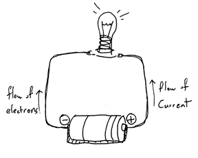
◾ Voltage : Electric potential difference between two points / Produces force to move electrons / Measured in volts(V)
※ Ohm's law : V=IR
◾ Current : Flow of electric charge / Current oscillates – can be measured by oscilloscope / Measured in amperes(A), aka amps/ 1 A = 1 coulomb
◾ Electrical Charge : Physical property of matter that causes it to experience a force when placed in an electromagnetic field / Two types exist; positive and negative (commonly carried by protons and electrons respectively) / Like charges repel
◾ Watt: Unit of power / 1J per sec
※ Generally black represents negative & Red represents positive.
※ Conservation law of electrical charge : "Total electric charge in an isolated system never changes."
※ Electrons flows to neg(-) to pos(+), while current flows to pos(+) to neg(-). The fact that current is the flow of electrons & electrons flow from positive to negative terminal was revealed after the flow of current was fixed.
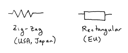
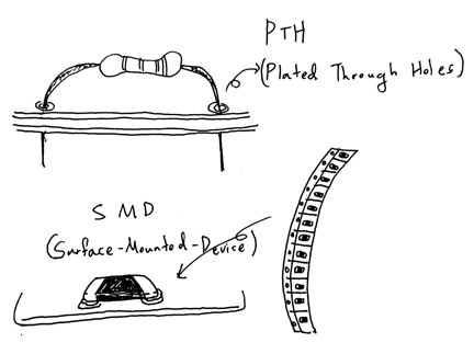
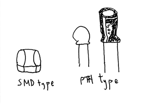
◾ Resistor : has a specific electrical resistance / used to control the flow of electrons / PTH(Plated Through Holes) vs. SMD(Surface-Mount Device)
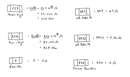
※ How to read a value of resistor
The drawing below explains how to read a value of SMD-type resistors. You may need a magnifying glass to check the digits on a resistor because SMD-type resistors are designed to be tiny as possible.
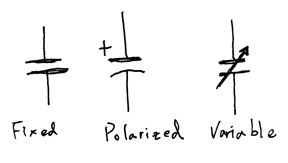
◾ Capacitor : used to store the energy of circuit / used to control the flow of electrons / has two terminal components and dielectric separates them - there is no connection between two sides, so the energy can be stored. / Polarized(; has one-curved plate) vs. Non-Polarized
※ Capacitor vs. Battery
1. Capacitor charge or discharge a lot faster than battery.
2. Battery of same size can store much higher E.
◾ Inductor : oppeses a change in current / stores energy in a magnetic field, which is generated by the flow of current / Higher inductance = More resistant to changes in current / measure in Henries(H) / 'L' stands for inductor
◾ IC : Integrated Circuit Chip / semiconductor which has specific function / cheap, spends low energy
◾ Amplifier : amplify signals / ex) transistor
◾ Voltage Dividers : used to intentionally induce voltage drop
◾ Hartz : a unit of frequency
b) Get Started with Eagle
Sparkfun tutorial easily descripts how to design PCB using Eagle in a two-step process:
1) Design your schematic, and 2) Lay out a PCB based on that schematic.
To design a modified echo-hello world, I used Autodest Eagle, which is the most used schematic editor and has intuitive layout.
Download Autodesk Eagle,
and get a library 00fab.lbr(Click the right button and save the library in C: > Eagle > cache > lbr).
Open New Schematic file in Eagle Control Panel (File > New > Schematic).
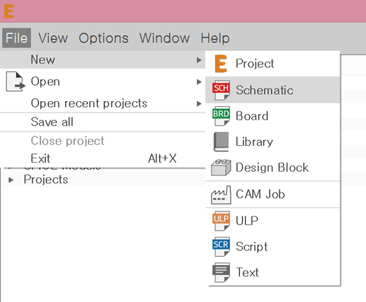
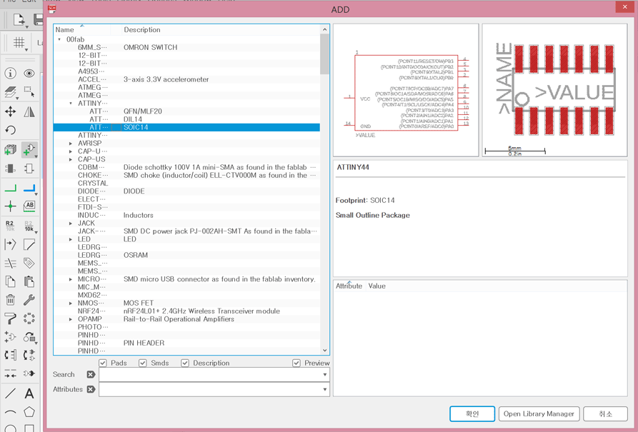
Open library manager (Library > Open Library Manager) and add 00fab.lbr (In Use > Browse).

Click 'Add part' on left bar and find the proper components in 00fab.lbr to redraw echo-hello world.
c) Redraw echo-hello world
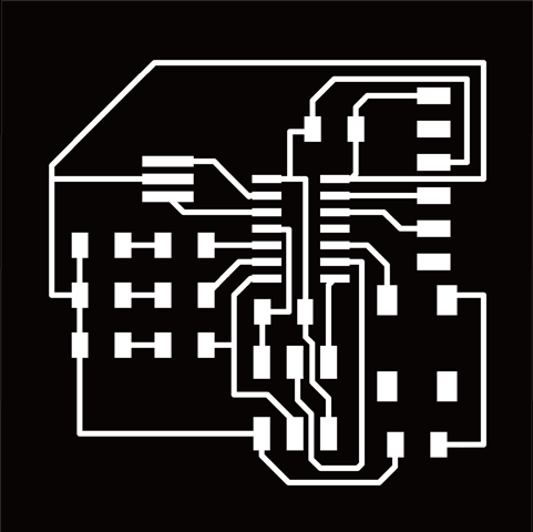
An original version of echo-hello world looks like this (Note that I dropped some detail parts of components):
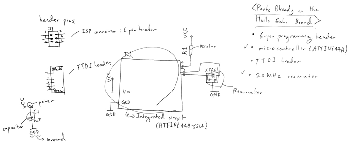
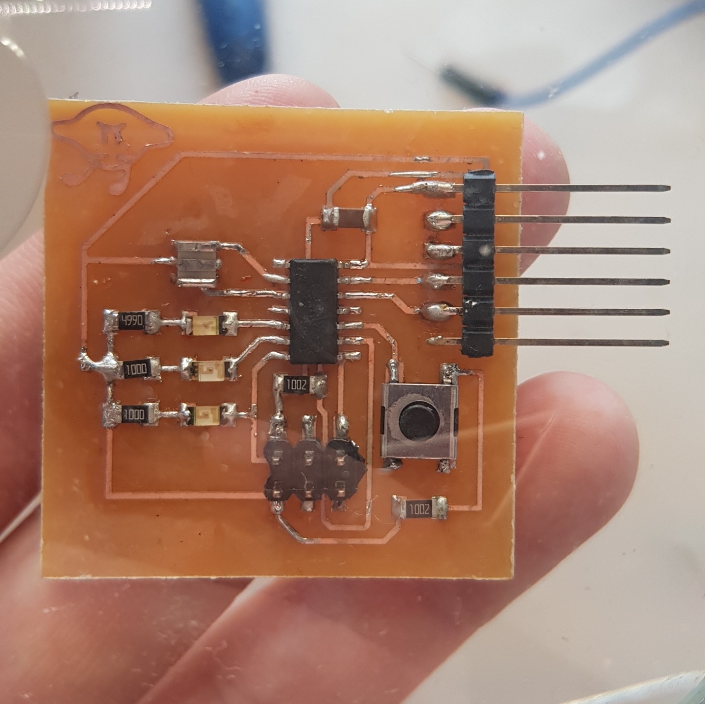
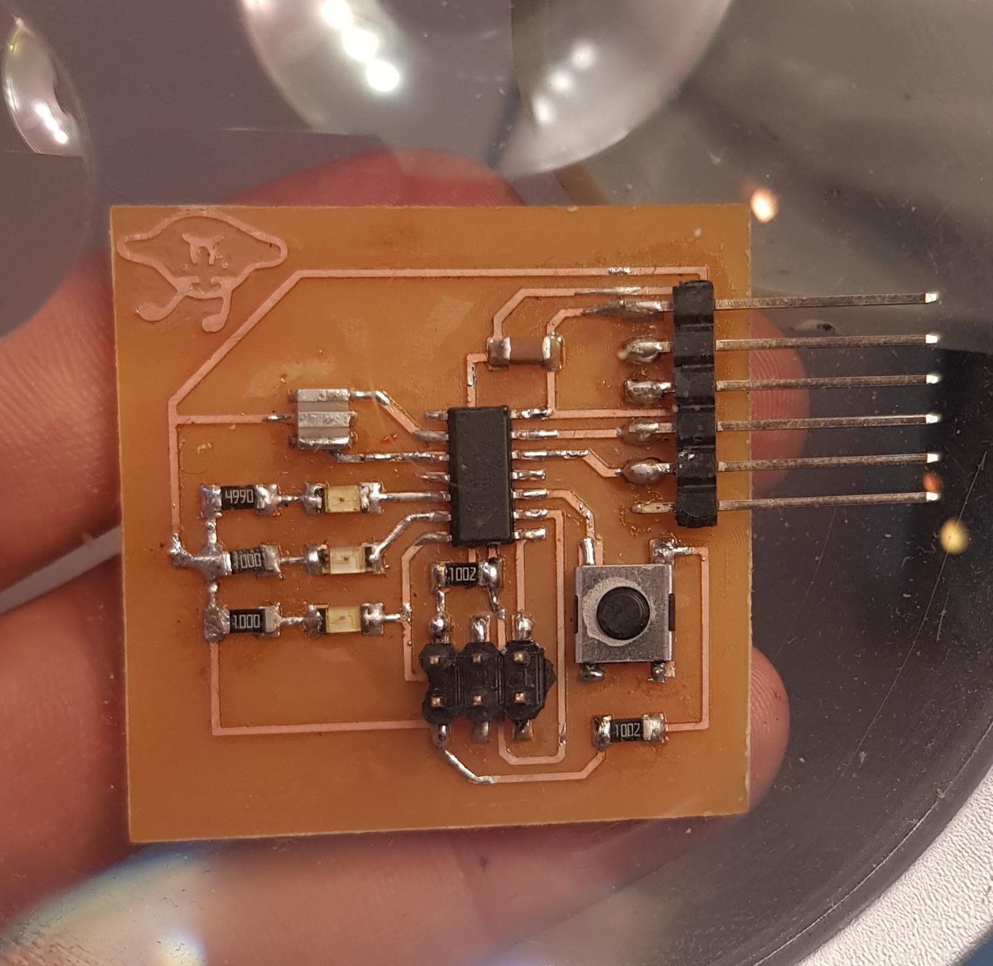
As it's summarized in the pic above, total six components (; 1) 6-pin programming header, 2) micro-controller (ATTINY 44A) 3) FTDI header, 4) 20MHz resonator, 5) 10k resistor, and 6) 1uF capacitor) are required to complete an original ver. of echo-hello board. After placing these parts, I added three LEDs of different colors and a switch to make an extended version of echo-hello world.
▣ List of components on the extended ver. of echo-hello world
◾ 6-pin programming header
◾ micro-controller (ATTINY 44A)
◾ FTDI header
◾ 20MHz Resonator
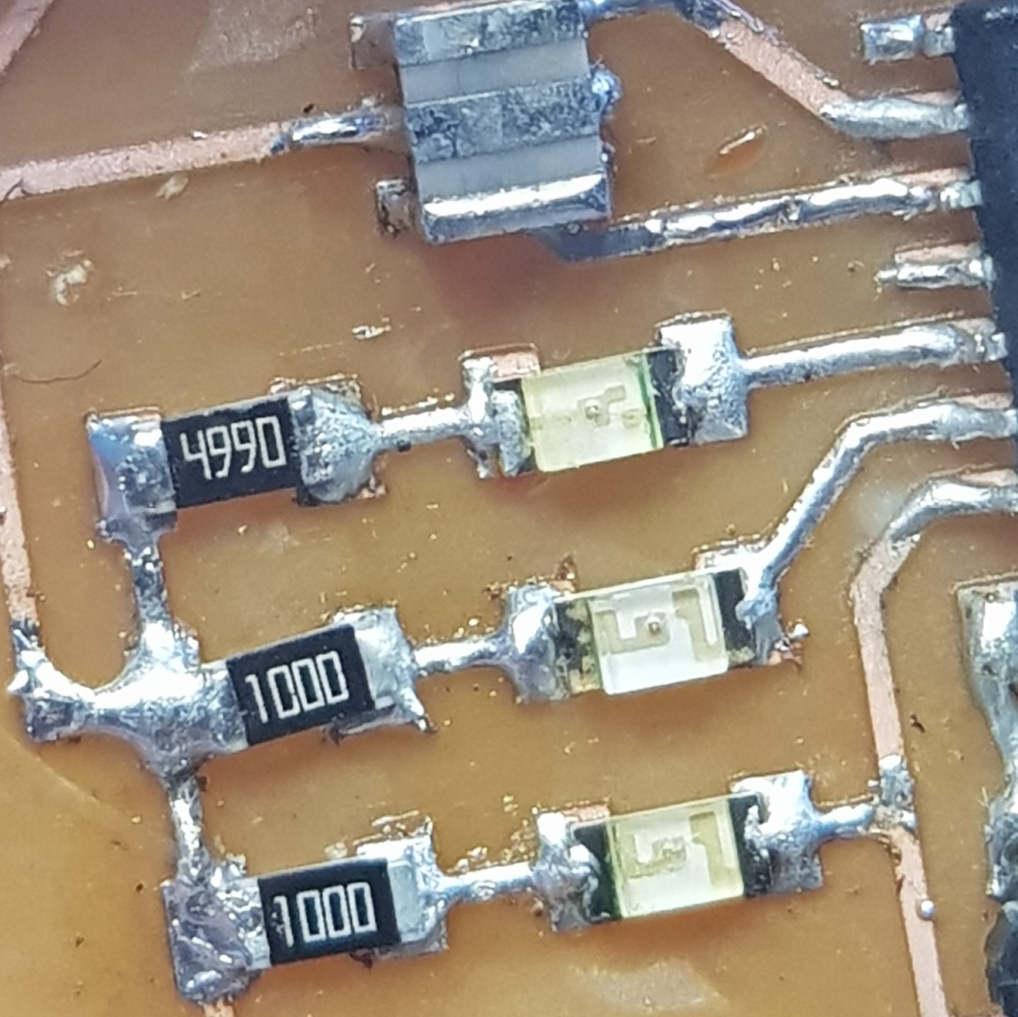
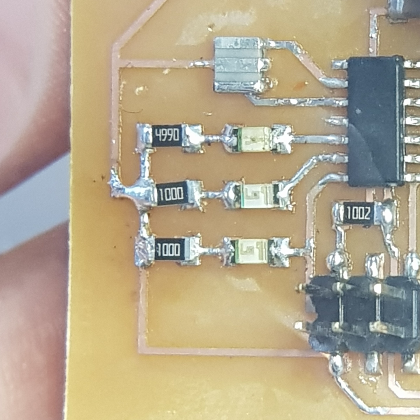
◾ 10k Resistor (x4) → ◾ 10k Resistor (x2) & 100 Resistor (x2)
◾ 499k Resistor
◾ 1uF Capacitor
◾ LED red
◾ LED green
◾ LED blue
◾ switch
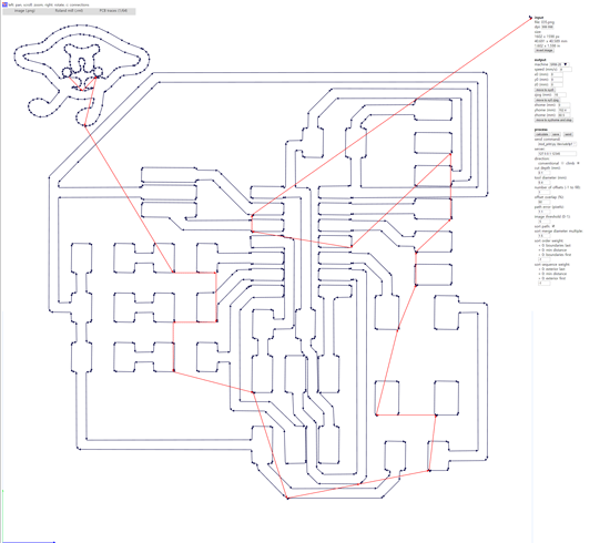
And the schematic looks like this:
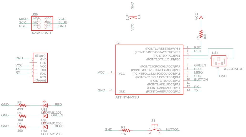
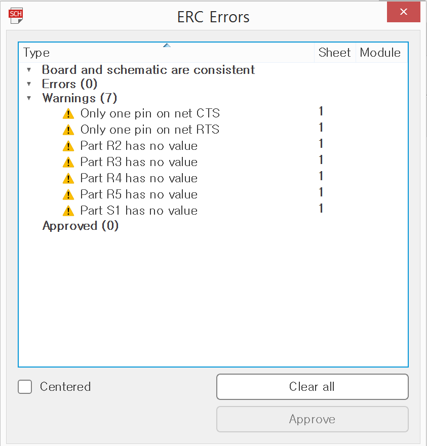
Check if there is any critical errors in the design (Tools>ERC). I did not have any issues that must be fixed, but there were some warnings - mostly about not fixing the values of resistors.
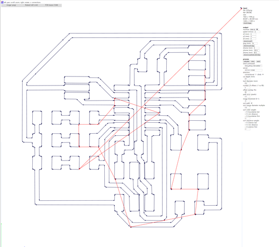
After finishing the design, press the button with red and grey on tool bar to switch the mode from SCH (; schematic) to BRD (; board). All the components connected with yellow lines will be in the corner tangled. Start to lay out the components - Place IC first as it has lots of connections with the others. Using 'Route' on the left bar, the parts can be actually connected in thick red line - Configure the width (; 12 ~ 16) and grid size of route.
For me, making routes was really tricky. I spend a day to connect more efficiently.
I tried to make short paths as possible to reduce unnecessary spaces on the board and broaden the space between the lines.
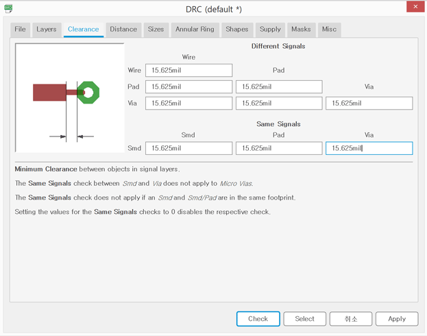
In this step, check if the space between the lines is too small - Use DRC like this (Tools > DRC):
There are two ways to get help with making routes : 1) Autorouter (on left bar), and 2) Zero-ohm.
Autorouter literally makes routes automatically, but I do not think it's really helpful in that you have to fix the routes anyway.
If it seems impossible to make connection in design step, solder a 0-ohm resistor to connect one to the other over a line.
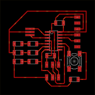
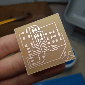
Fortunately, I did not use any alternative methods and an image of the board looks like this:
d) Export an image file of designed schematic
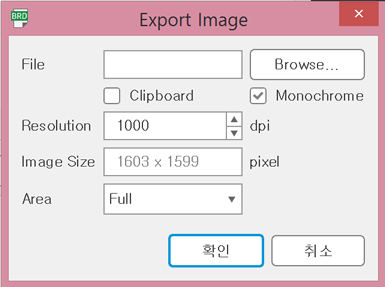
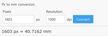
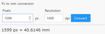
I never expected that this step would cause so much trouble. In the process of exporting an image of schematic in Eagle and later in Illustrator, the size (width and height) changed for some reasons. On Monday (actually I planned to finish my whole assignment on this day... Impossible to keep to the schedule as there are always unexpected barriers...), I finally solved the problem by setting the same value of dpi in every programs (Eagle, Illustrator, fabmodules), then I realized that it is so basic principle when dealing with an image.
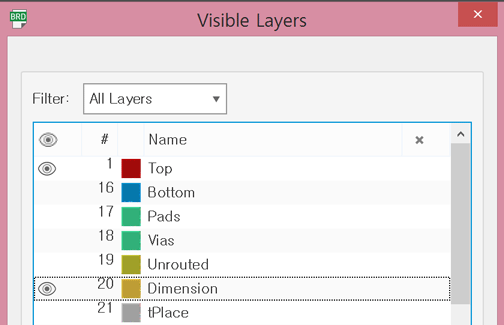
Before exporting an image, click 'layer settings...' on left bar and hide every layers except Top (1) and Dimension (20). The board should have lines (red) only, like a PCB.
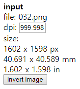
Export a schematic as an image file (File > Export > Image). Set the resolution as 1000 dpi. Check the size of image at this point. Convert the unit from pixel to mm using any converter on internet so that you can weigh up the actual size of a board.
e) Check & Modify an error of image file
So many images went to trash before this one:
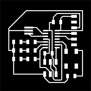
Somehow some lines slightly poped out though it can be barely checked. I modified those parts and this is the next version:
In fabmodules, import an image file and check the milling path by setting the number of offsets to 1. If there is any part of board that is expected to be uncutted in an end milling machine, modify in illustrator.
Again I checked the resolution and size of an image, and it seemed fine.
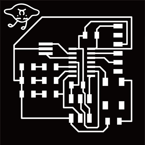
I added the character in the corner. Also made an image for the outline. Click each image to download png files :

Again, I simulated the milling process for both files, and saved each of them as rml files. An interior design should be traced with an end mill of 0.4", while an outline design should be cutted with an end mill of 0.8". To save each files with proper configuration, find more information on week 5_electronics production. Click each image to download rml files :
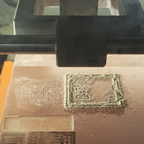
f) Milling PCB
For detail explanation about milling PCB, again, consult the week 5_electronics production. I also suffered in this step - spend a day milling PCB with a broken end mill. Always have to check the status of whole device and its parts carefully... I failed several times, but finally, I got satisfying result - on Tuesday.
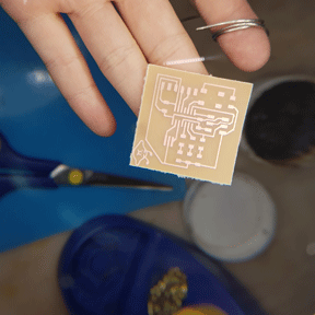
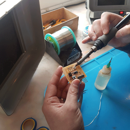
g) Soldering
I was so bad at soldering when I tried making ISP two weeks ago - the part of circuit was burned and I struggled to fix it, but after all it didn't work. I shared this problem in asian meeting, and instructors told me to use a proper temparature and heating time to solder. So I set the temparature up to 250 (last time it was 450), and heated the circuit with soldering device for 1 or 2 minutes. It was much better this time.
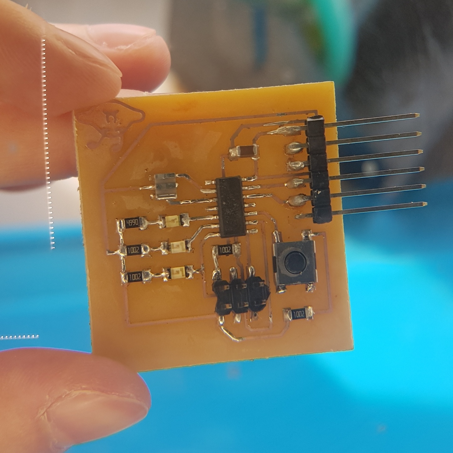
(Later I found out that I connected wrong resistors to green and blue LEDs.)
2. Study Arduino & Test and Simulate the operation of PCB
a) Get started with Arduino
I downloaded Arduino and followed Program an ATtiny44/45/84/85 With Arduino. When I tried to upload code on the board, the error occurred - while compling & burning bootloader. My instructor checked my board and advised me to "Debug Hardware."
b) Debug Hardware
Using flux liquid, I tried to remove beads-like metals on the board and make the parts look more clean. . flux / smoke absorber 조금 잘 안됐던 부분들이 shiny하고 더 작고 정확하게 바뀜