Electronics Production
1. Characterize the design rules for your PCB production process.
The hardest point of this week was to deal with tiny, fragile materials. My instructor told me to please be careful when changing the end mill in the milling machine, as the end of the end mill can easily break. Also he gave us a plastic compartment to keep the tiny electrical components safe and properly. Thanks! :-)
List of Machine, Materials, and SWs that I mainly used for this week's assignment
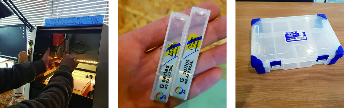
◾ Roland SDM-40A: End milling machine in FabLab Seoul
◾ Fab Moduless: Convert .png file to .rml file & Set the output conditions such as machine type, milling speed and zjog
◾ V Panel: Set the origin and coordinate system to start milling
◾ Milling bit: 0.4mm(1/64") to trace & 0.8mm(1/32") to cut the outline
◾ FR-4 PCB(Printed Circuit Board)
◾ Electirical componenets for FabTinyISP
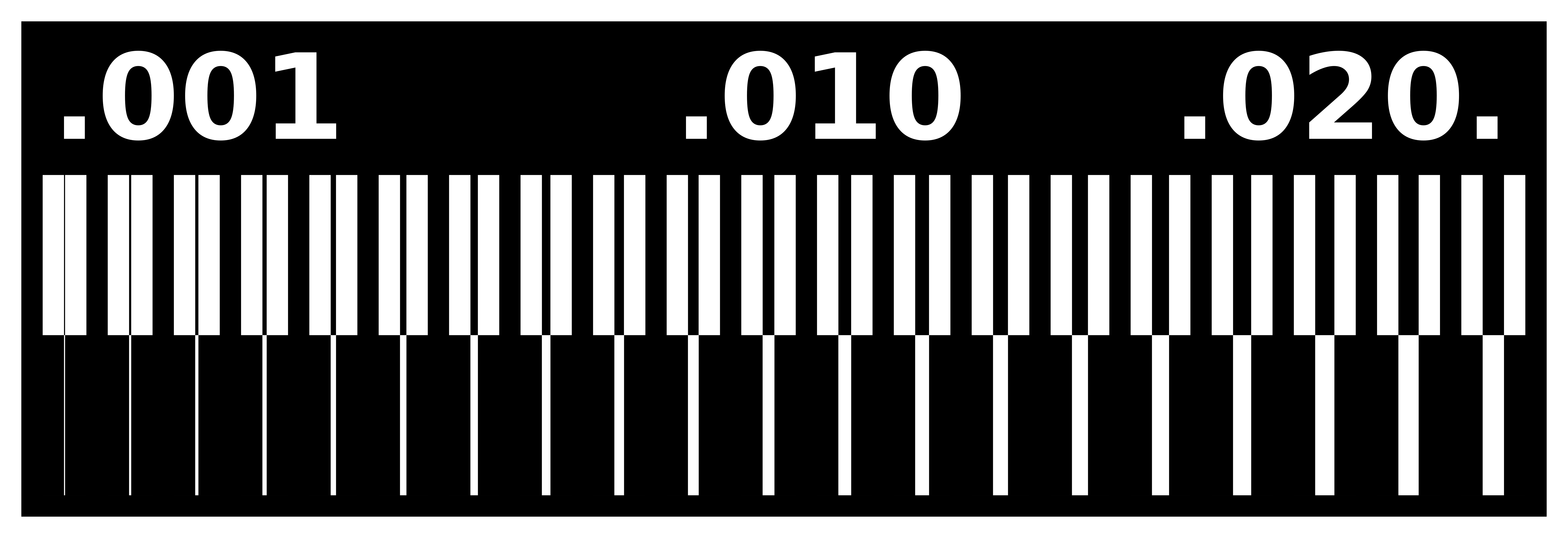
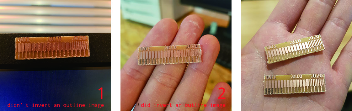
First, I did the line test to check the quality of an output of the end milling machine that I am going to use. I originally downloaded the .png files for line test from the Fab Academy's schedule page-week 5. Click the images below to download .rml files that I made using Fab Moduless. You can directly add these files in V Panel by pressing CUT button. More explanation on using V Panel will be continued.

I did it twice. At first, I forgot to invert the outline image file in Fab Moduless, so an edge of the design was cut too much. Remember that the black part of an image is cutting. After I modified the settings to invert an outline image and newly saved the .rml file, I expected the output to be ... something more different. Maybe it slightly changed but I could barely recognize it.
2. Milling PCB.
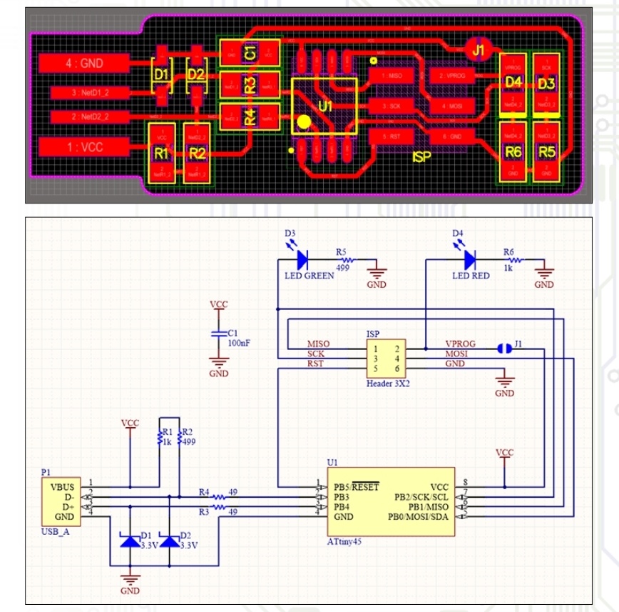
I used a “Brian PCB Design”, you can download the .png files below. Now I will explain how to convert these files to .rml files using Fab Moduless program.
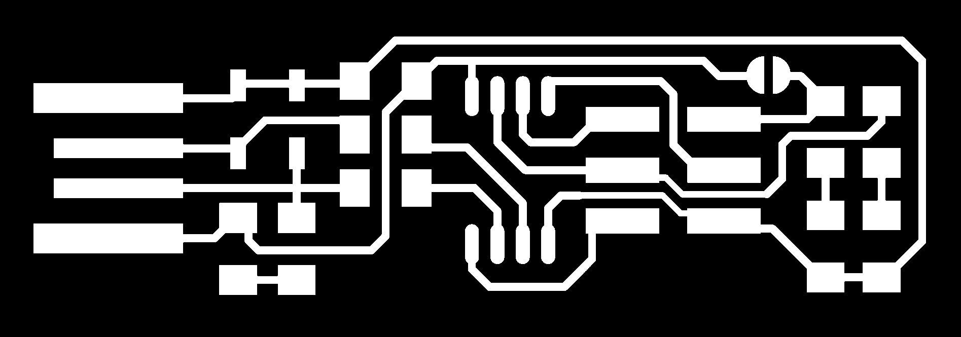

First import .png files and set an out format as Roland mill(.rml). From this step, different options are required for each file to trace or cut. I configured the output(speed: 0(mm/s) / x0, y0, z0: 0(mm) / zjog: 10 to 12(mm)) and process(number of offsets: -1 sections to trace.
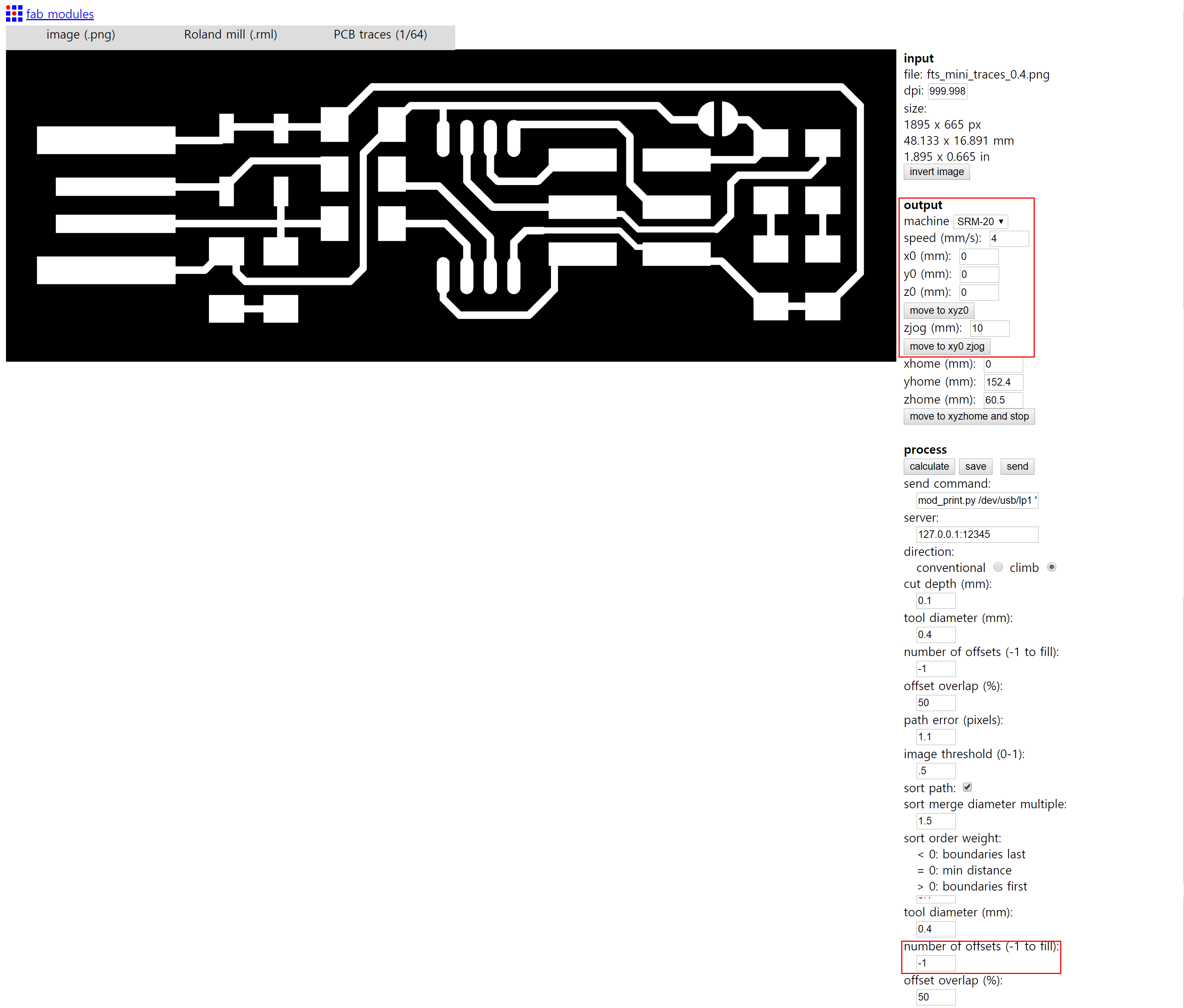
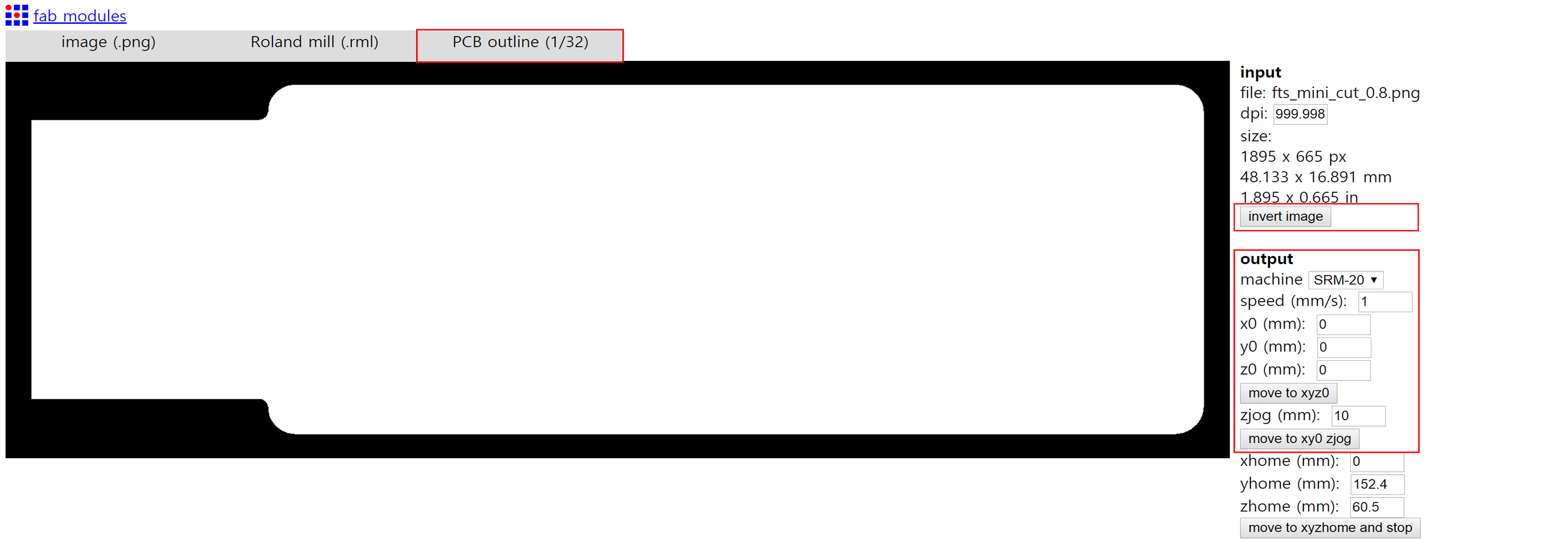
And I configured the input(press the button "invert image") and output(speed: 0(mm/s) / x0, y0, z0: 0(mm) / zjog: 10 to 12(mm)) sections to cut the outline. Save the .rml file if all settings is completed.
Now go to the computer that is connected to an end milling machine and open the V Panel. Before changing the origin and setting the coordinate system of an end mill through V Panel, you should carefully change an end mill to the proper one - As I mentioned above, if you wanna trace, use the milling bit 0.4(mm). If you wanna cut an outline, use the 0.8(mm). Check twice if an end mill is tightly fixed to a machine since it will definitely break when it falls down. Set origin point while continually watching the movement and current position of an end mill - Consider the size of the image that will be printed on the board. When moving in z direction, set the cursor step to X100 - to prevent the sudden crush between an end mill and a circuit board from happening. If you find the proper position to start milling the design, set the position to an origin by pressing the X/Y and Z buttons below the "Set Origin Point".
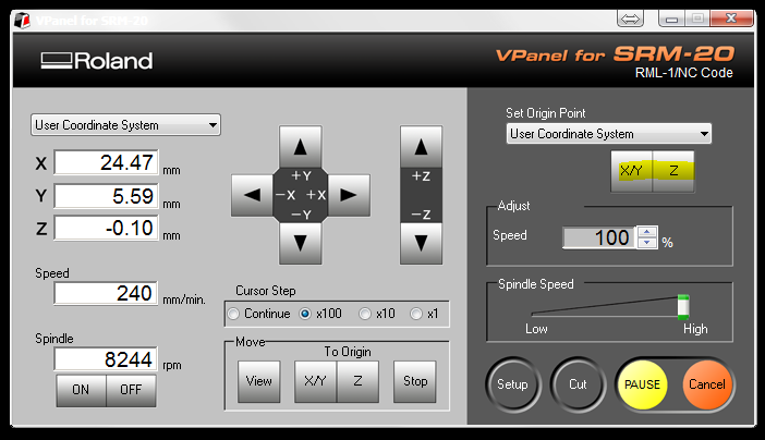
If all settings is completed, press +Z button two or three times to safely start milling - On this step, the X and Y position should be 0(mm), and the value of Z will be, maybe 2 or 3(mm). Import the design by pressing the CUT button on the panel, and finally the machine is really ready to mill the design on the circuit board.
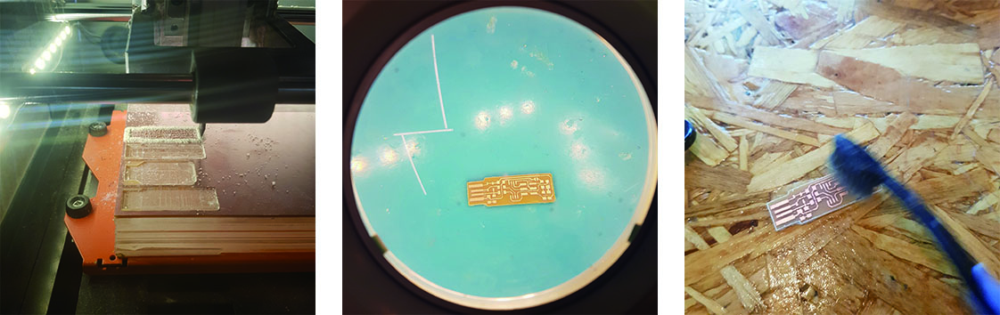
The PCB wasn't neat, but after brushing the surface it looked pretty fine for me. I also used a cutter to remove unnecessary parts - excess copper.
3. Soldering electronic components on PCB.
By following the documents on FabAcademy website, I soldered electronic components. I don't know anything about electonic things...so my instructor recommended me to watch some videos(and I will...but not yet...).
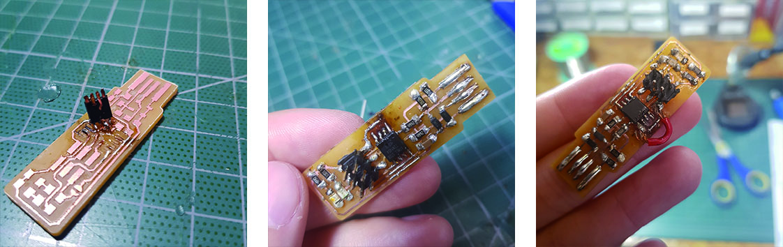
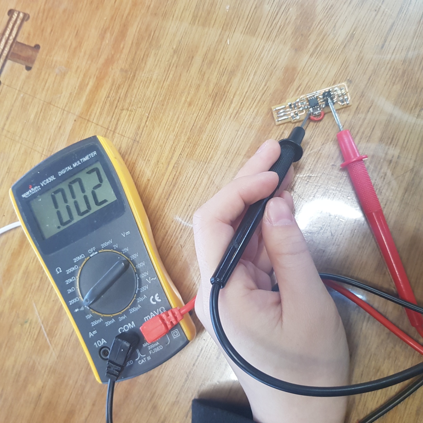
I did everything twice because I always failed on the first trial. The first PCB that I made became totally useless in just... about 30 minutes (picture on the left side), because I completely took off the part of the printed circuit where ATtiny45 should be placed. - Actually I was trying to took off ATtiny45 with melted legs. I did the same mistake on my second trial. This time the legs didn't melted but I burned the printed circuits where ATtiny45 should be connected! Instead of taking off the components (or going home), I connected the circuit using a short red wire (picture on the right side). I know it looks ugly(because I am terrible at soldering...Need to practice from now on :-)), but when I checked the continuity of the componenets using the multimeter, it seemed to work normally. On asian review, the instructors advised me to check the temperature and know the proper time to solder.
Expecting LED to turn on, I connected FabTinyISP to my laptop through an ISP cable, but instead smoke billowed out. To find out the cause of trouble, again, I checked my ISP with digital multimeter and still the continuity of each components seemed just fine. So I thought the cause of smoke was loose wire connections and decided fix the connetion between a red wire and ATtiny45.
4. Programming
5. Result of this week
Probably everyone is busy now, but I was unsually busy last week... I will do the programming for the upcoming week. So until now(19-02-20), the picture below is all I got for the result of this week...:-)