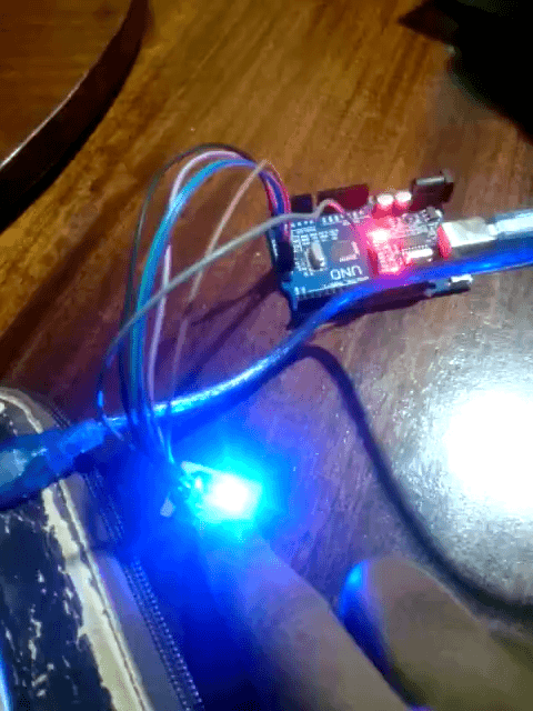
The goal of this week is to design a circuit composed of the push button and LED. To archive this objective,I used different tools such as EAGLE software to design the circuit, SRM-20 Machine to print my board. Thereafter, I used Arduino IDE software to program the board.
Group assignment
Use the test equipment in your lab to observe the operation of a microcontroller circuit board
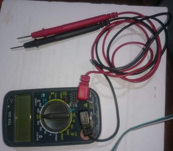
The purpose of the group assignement is to check the equipements available in the lab to see what’s going on in a circuit board. For this we have two main equipements :
- Multimeter
- Oscilloscope
In this assignment we tested Attiny 45 microcontroller board, we cheched both the input and output with the help of the multimeter and oscilloscope.
Testing the input and output voltage of Attiny45
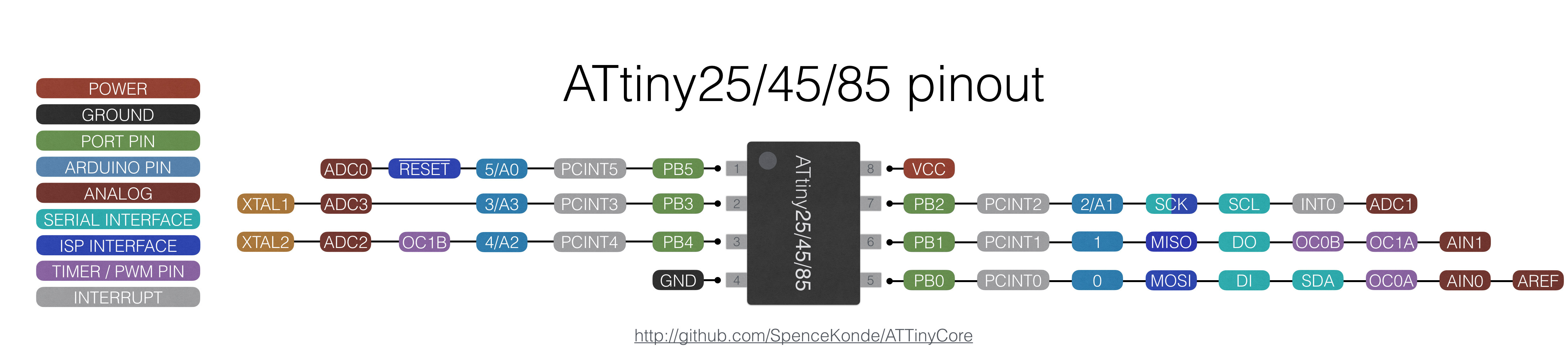
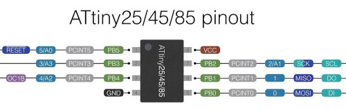
With this board we are going to test both input and output voltage. By refering to the datasheet, Attiny 45 microcontroller has 8 pins and one pin can play more than one role as indicated on the diagram below.
 s
s
Testing Attiny45 with button
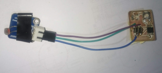
Testing Attiny45 with LDR photoresistor
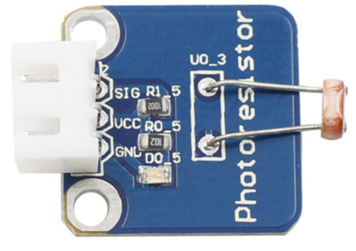
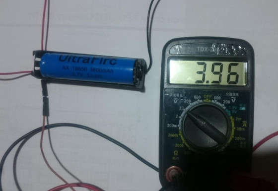
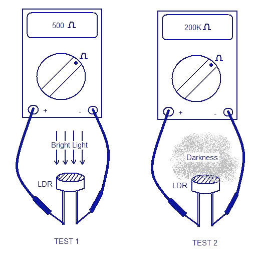
LDR (light dependent resistance) can be very easily tested by using a digital multimeter. We all know that the resistance of an LDR varies according to the light falling on it. At bright light, the LDR resistance will be around 500Ohms and at darkness the resistance will be around 200K. For a proper diagnosis we need to measure the resistance of the LDR at bright light and at darkness.
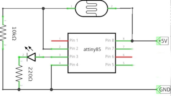
According the datasheet, the ATtiny25/45/85 features a 10-bit successive approximation Analog to Digital Converter (ADC). The ADC is connected to a 4-channel Analog Multiplexer which allows one differential voltage input and four single-ended volt- age inputs constructed from the pins of Port B. The differential input (PB3, PB4 or PB2, PB5) is equipped with a programmable gain stage, providing amplification step of 26 dB (20x) on the differential input voltage before the A/D conversion.
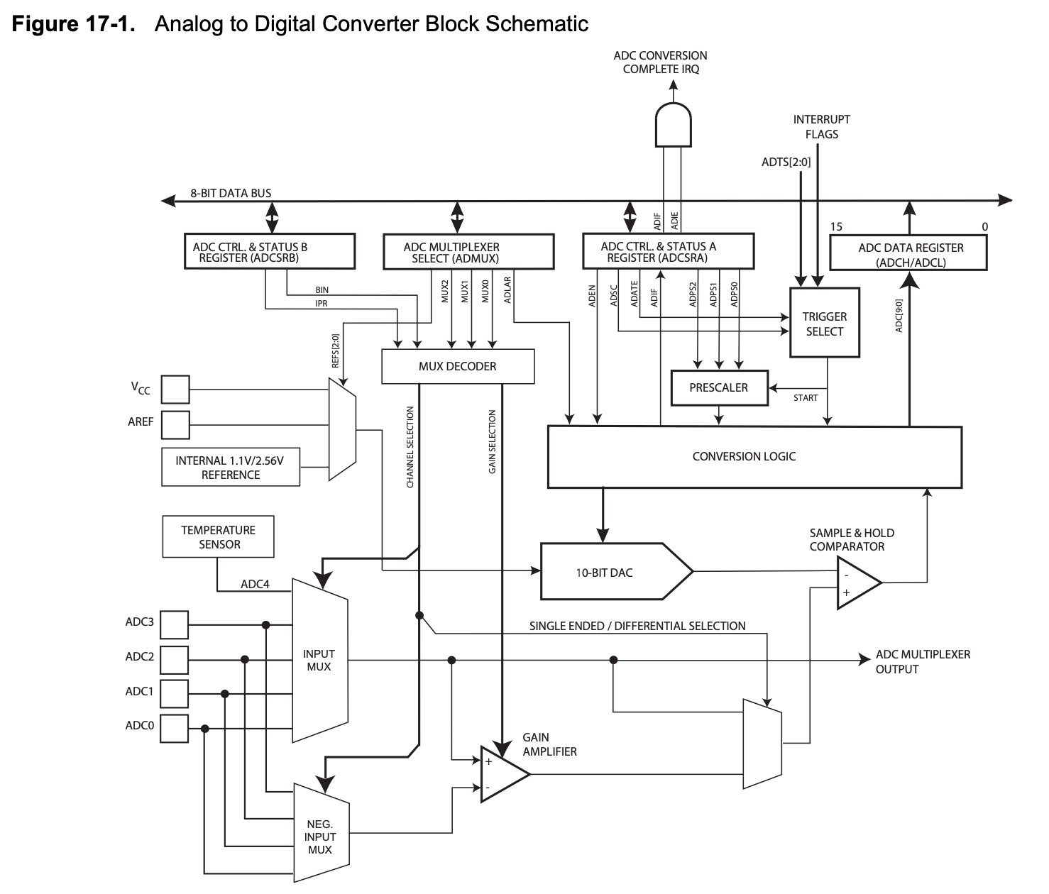
Internal reference voltages of nominally 1.1V / 2.56V are provided on-chip. Alternatively, VCC can be used as refer- ence voltage for single ended channels. There is also an option to use an external voltage reference and turn-off the internal voltage reference.
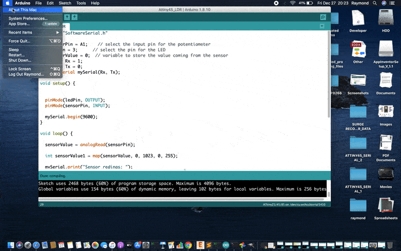
In this sketch it is indicated that the LED on the board will turn ON if the reading value from sensorPin ADC pin (A2) is equal or greater to 500, we observed that the minimum reading is 0 and maximun is 1023 because the ADC pin convert analog readings from LDR to digital (10 bits).
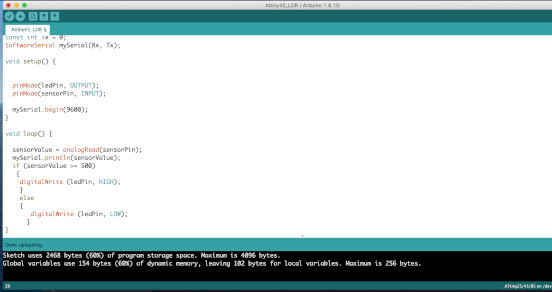
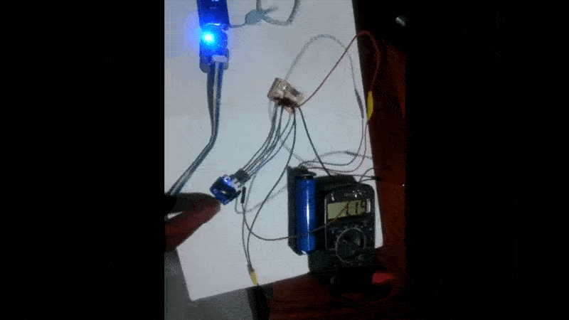
The maximum voltage measured at the analog pin is 3.55 Volts when the LDR is exposed to the darkness and the minimum voltage measured when the LDR is subjected to bright light source is 1.18 Volts. We observed that the LED changed from OFF to ON state when the voltage gradually increased to 1.89 Voltage and above.
DC Voltage Measurement
Theorically, the analog voltage ADC reading Value is converted to Voltage with the help of the below formula

Individual assignment
Designing process
To design my first circuit, I first selected the necessary electronic devices.
Used components:
- Attiny45
- Push button
- Resistor 10K (2) & 490 Ohm for LED protection
- LED diode
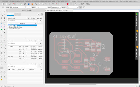
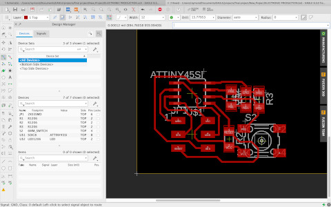
Designed Circuit
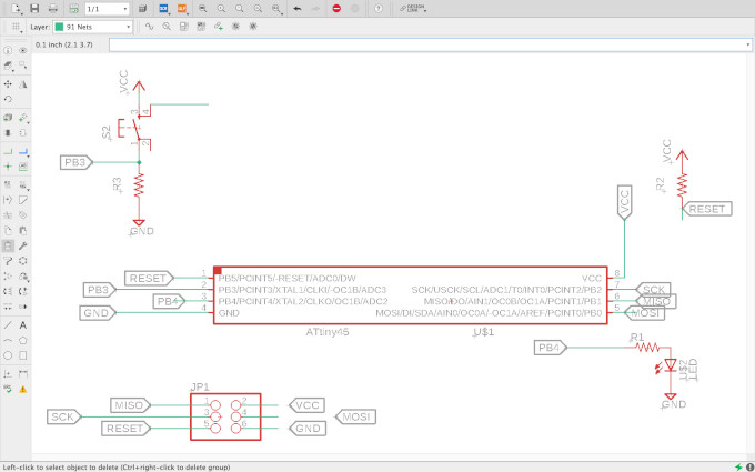
This circuit was designed with the help of the Autodesk Eagle software. The Attiny45 has only 8 pins but to fullfil this assignment I used only two pins. Push button was connected on PB3 pin and is working as the input pin and LED is connected to the PB4 pin and it operate as the output pin.
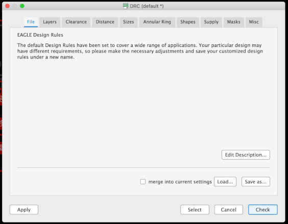
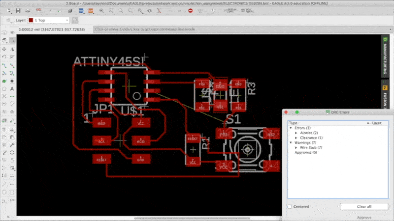
ERC and DRC Check
Eagle provides two tools that help you to check whether your board is correct or not: a.) electrical rule check (ERC) and b.) design rule check (DRC).
a.) The ERC checks e.g. for any open or overlapping pins and ports on your schematic and will give out these errors. b.) The DRC establishes a set of boundaries for trace widths, component spacing, via diameters that you can check for your board.
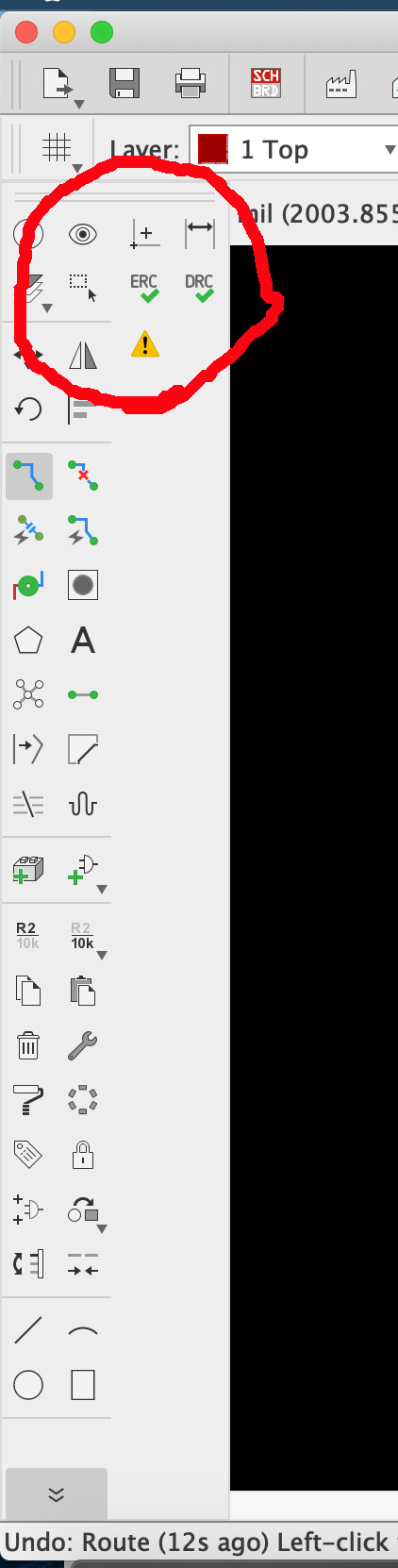
When you choose one of the tools this window will pop up. Simply click on the button 'Check' and the check will be executed.
The ERC check did produce warnings. But these warnings are not crucial to not make my board work. It just reminds me that I have not added values yet.
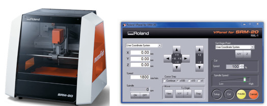
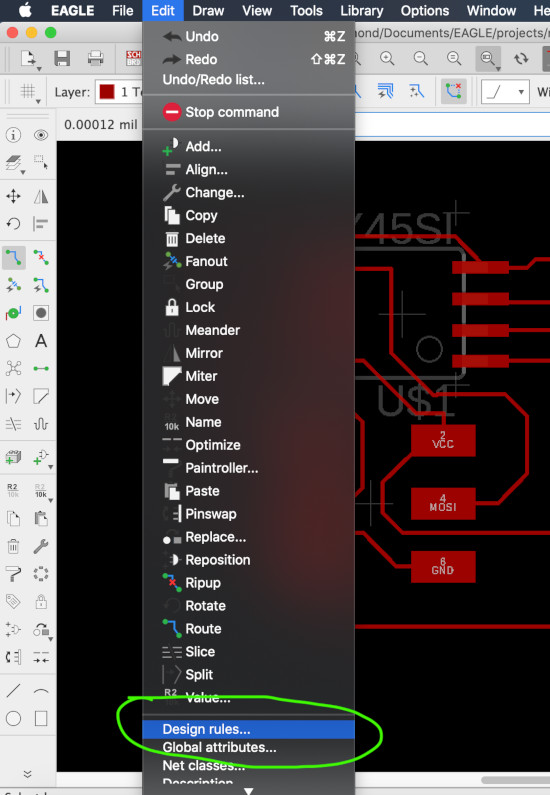
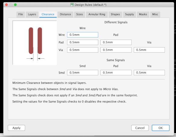
Now we have to set the design rules for Roland Mill SRM-20 . For that I open "Design rules" under "Edit"
Then we need to set the Clearence , we are using 1/64 bit for milling so here the trace will come around 16 mill. The minimum clearance cannot be less that the diameter of the milling bit that you plan to use.
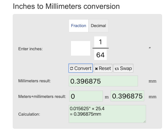
After converting the bit size 1/64 inch to millimeter, I realised that it will much better to use the clearence of 5 mm.
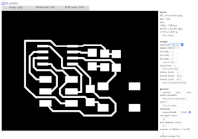
Milling files
The milling files was generated from monochrome .PNG pictures. Here are the steps of creating Milling files with the Fab Modules.
traces and Outlines

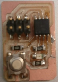
PCB printing and soldering components
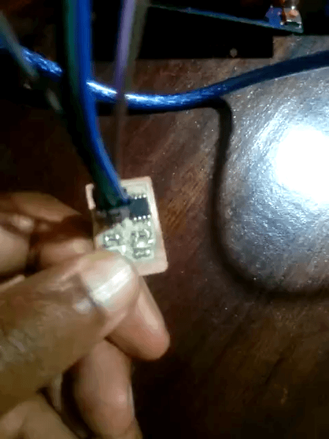
After printing the board, the next step is to get my hands dirty by soldering all components to the board.
Programming the board
After succesful soldering the board, the next step is to program the chip. To program the board, I used arduino UNO as an AVR In System Programmer (ISP). This allowed me to burn a program onto a new chips (Attiny45).
Arduino as an In-System Programmer or ISP
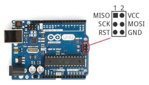
Since ATtiny must be programmed through the SPI interface, ATtiny can be burned through Arduino Uno's SPI interface.
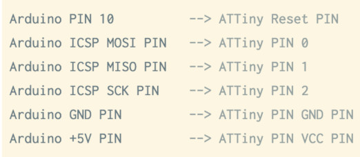
Programming any AVR microcontroller six wires are needed. Three of these wires are referred to as the Serial Peripheral Interface (SPI) and are the Master In - Slave Out (MISO), Master Out - Slave In (MOSI), and Serial ClocK (SCK). The "Master" is the ISP or the device you are using to program the AVR chip. The "Slave" is the AVR chip being programmed. The other three wires are for the 5V power supply (VCC), Ground (GND), and Reset (RESET).
add ATtiny expansion pack to Arduino IDE
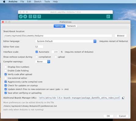
Attiny45 didn’t come with Arduino IDE and the next step is to integrate this board. You can install the ATtiny support using the built-in board's manager. Open the preferences dialog in the Arduino software.Find the “Additional Boards Manager URLs” field near the bottom of the dialog. Then, at the bottom of the pop up menu where you see "Additional Boards Manager URLs" you want to copy and paste "https://raw.githubusercontent.com/damellis/attiny/ide-1.6.x-boards-manager/package_damellis_attiny_index.json" (without the quotation marks).
Install the ATtiny Board Package
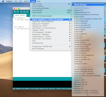
- From the Arduino IDE go to Tools--> Board-->Boards Manager
- A new tab will open and at the top of the tab type: attiny
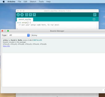
- Select Install on the Attiny by David. A Mellis
- Restart the Arduino IDE
- The ATtiny45 board should now be added ! Go to Tools--> Board-->Attiny45
To confirm that you have added support for the boards, navigate to Tools > Board and you should see ATtiny45 at the bottom of the list.
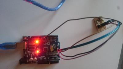
Connecting ATtiny45 with Arduino Uno
Now with all the above things ready we will start programming the attiny85. Connect the arduino uno to ATtiny45 using breadboard as below.
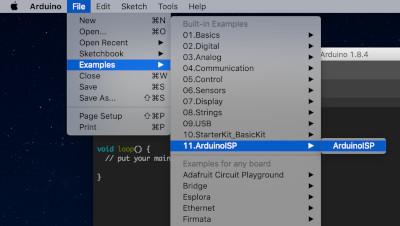
Since what we want is to be able to program the ATtiny45 from the Arduino IDE which requires to burn the bootloader to the ATtiny45 we will need to "prep" the Arduino fist by uploading the ISP sketch to it. In the Arduino IDE select File-->Examples--> 11. Arduino ISP-->ArduinoISP
pins configuration for both arduino (ISP/ISCP) uno and attiny45
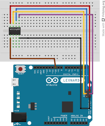
Connecting ATtiny45 with Arduino Uno
Making the ATtiny85 Arduino Compatible
Since what I want is to be able to program the ATtiny85 from the Arduino IDE which requires to burn the bootloader to the ATtiny85 I will need to "prep" the Arduino fist by uploading the ISP sketch to it. Now my Arduino is now an AVR ISP.
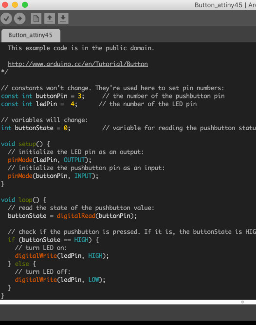
Coding and Uploading program to ATtiny45
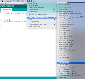
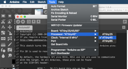
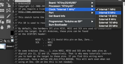
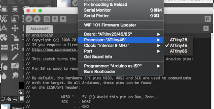
Now back to Arduino IDE. Select ATtiny under Tools -> Board. Then select ATtiny45 under Tools -> Processor. And select 8 MHz (internal) under Tools -> Clock.
By default, the ATtiny’s run at 1 MHz. You can configure them to run at 8 MHz instead, which is useful for faster baud rates with the SoftwareSerial library or for faster computation in general.
APLOADING THE PROGRAM TO THE BOARD
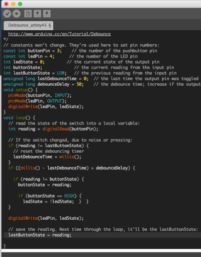
SWITCH DEBOUNCING
One of the major problems encountered when using push buttons and switches in digital electronics project is the problem of bouncing. When I press a button once it may register twice and when I press it four times, in a row, for instance, it may register just twice. This occurrence is due to a property of switches known as bounciness which is as a result of the physical property of the switches.
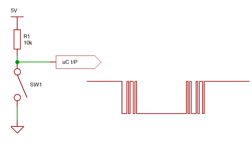
The debouncing is a tentative to mitigate this effect and remove any eventual spurious detection. There are two ways to debounce a push-button:
- in hardware, by filtering the input signal
- in software, by adding a dead time after the first detection.
To solve this problem, I used software debouncing technique. The code below demonstrate how to use debounce on the Atmega micro-controller by using push button. When button press it will stay HIGH State if press again it will stay at LOW State. This sketch uses the millis() function to keep track of the time passed since the button was pressed.