


Step 1: to design and prepare the board with its components.
to do so, we used EAGLE for creating the schematic then routing a path that connects the components.
First of all to start with EAGLE, we have to create a new project and activate it, so every shcematic or board created wold be part of the project.
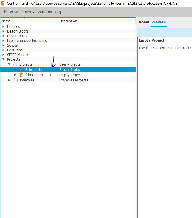
In the new project (named "Echo hello-world") we fist create a schematic file and open it.
There is a library provided by the FabLabs named "fab". We have to place this library in libraries folder in the EAGLE's directory.
After having the library, we start plotting our circuits following the schematic given by Fab Academy.
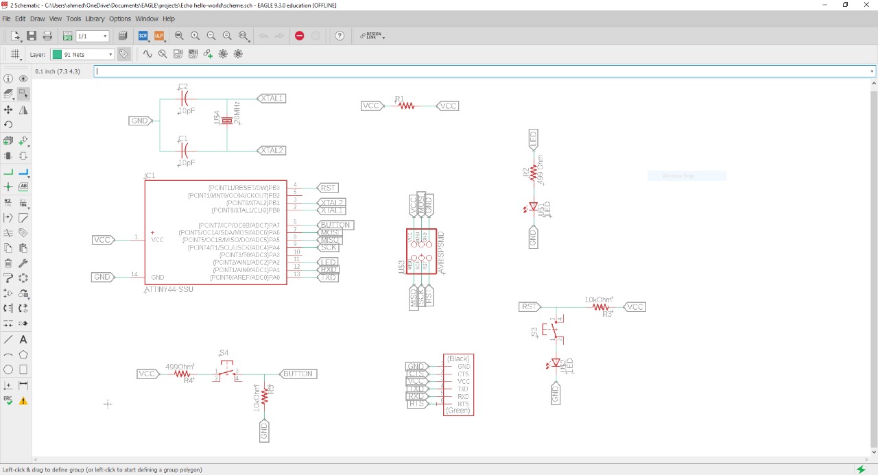
To understand how those components were selected, let's take a look on the circuits:
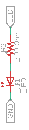
The LED is a diode which is basically a valve that lets the current pass by one direction only, and even tho this diode is light emmitter, it is still considered a component with very low power consumption that we can almost say it is like a wire. So to ensure that no excessive current will pass through as in short ciruits, we added a 499 Ohm resistor.
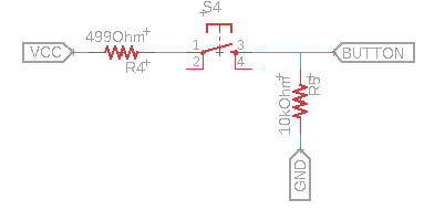
When the button is clicked, the button bin will read HIGH. But there will be a short ciruit, so we have to add a resistor just like the previous case with the LED. And when the button is not clicked, we have an open circuit. So to ensure that the button pin will read LOW, we have to add what is called a pull-down resistor between the pin and the ground.
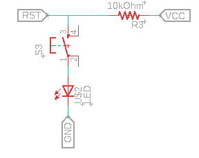
The reset button is connected in an opposite way comparing to the LED button because we want it to read HIGH when the button is not clicked. So we use a pull-up resistor to regulate the current. In the case of unclicked button, the current will flow from the VCC to te reset pin, passing through the resistor. And in the clicked button case, the current will go from the VCC to the ground through the LED, leaving the reset pin at LOW.
After finishing the schematic, we create a Board file in the same project. The components will appear in the board's window with a net of lines connecting between them.
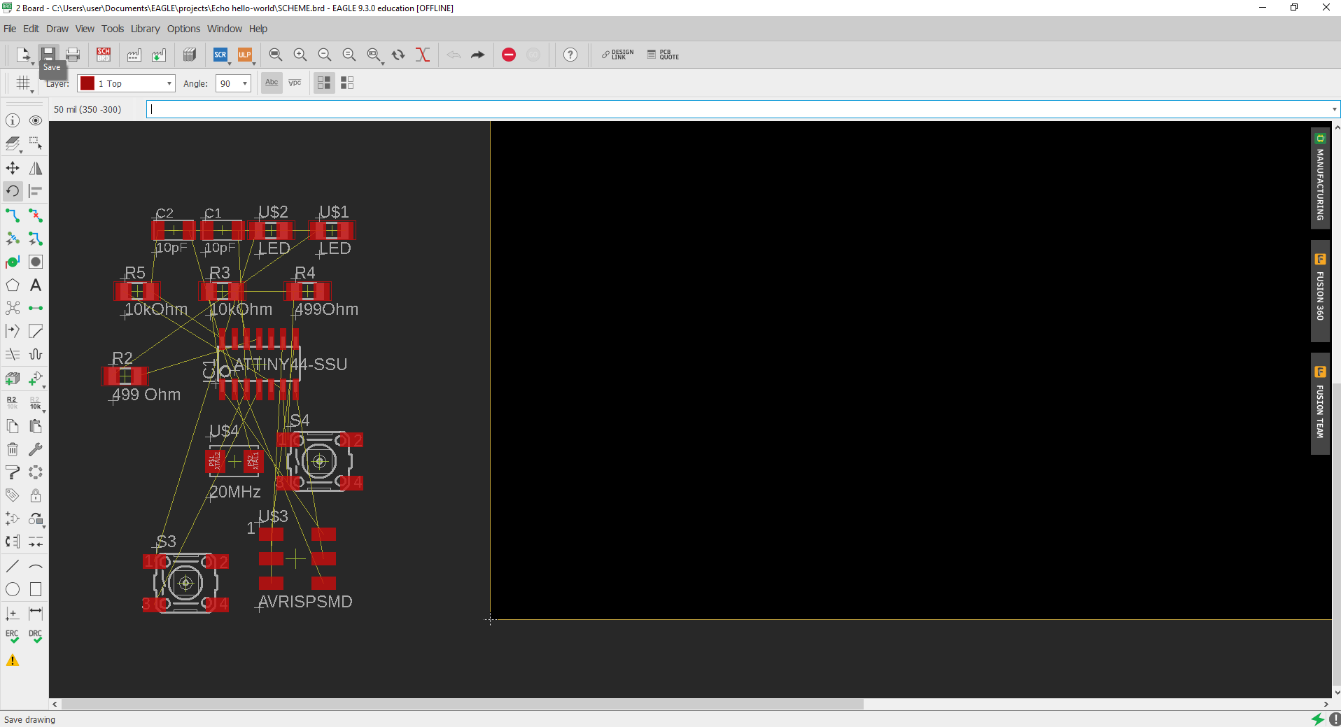
First of all, we try to arrange the components as possible then click on the Ratsnest from Tool's list.
Then start routing and arranging till you have a satisfying design.
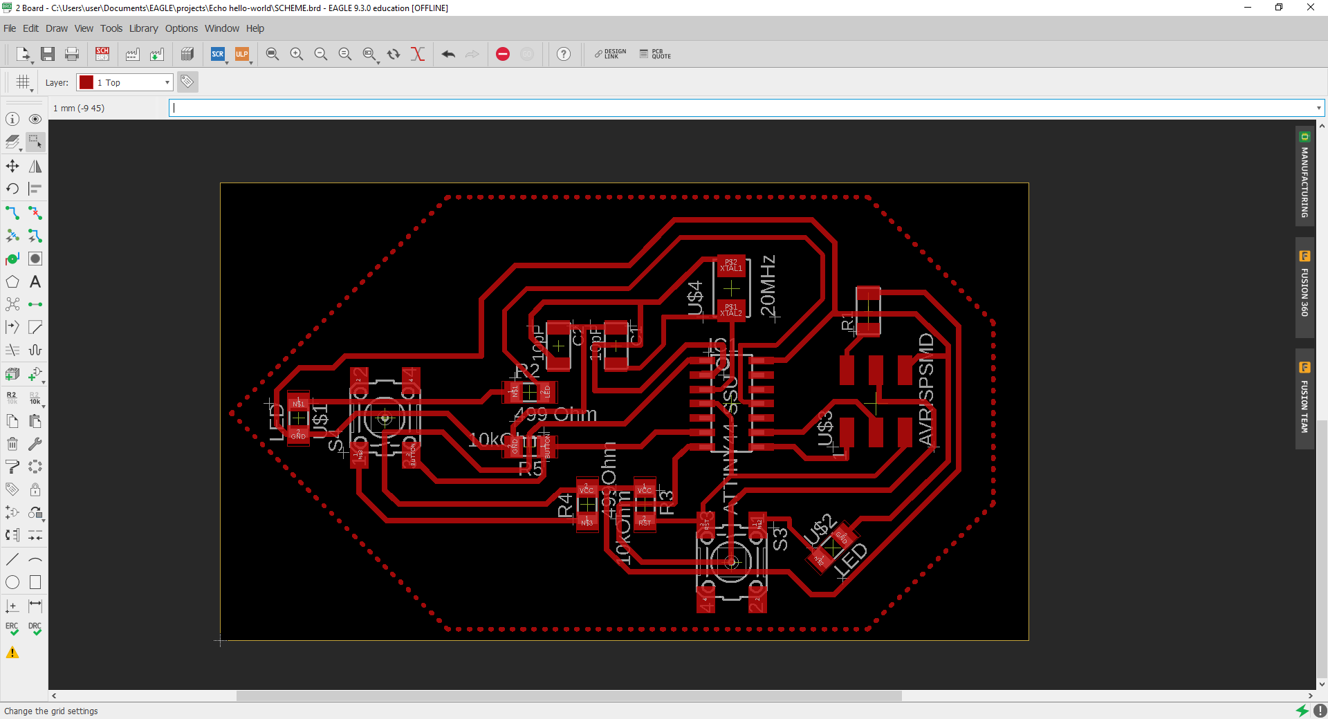
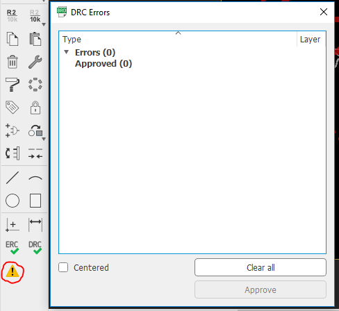
We can check if there is any error in the routing or a missing link by clicking on the button shown in the pictre:
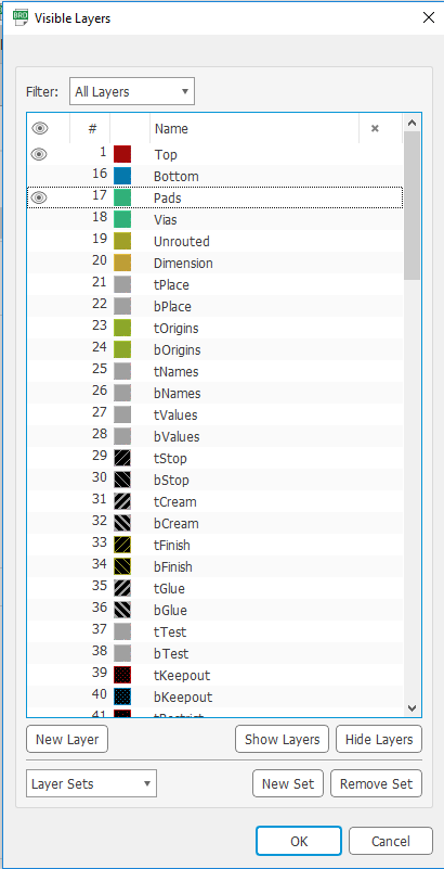
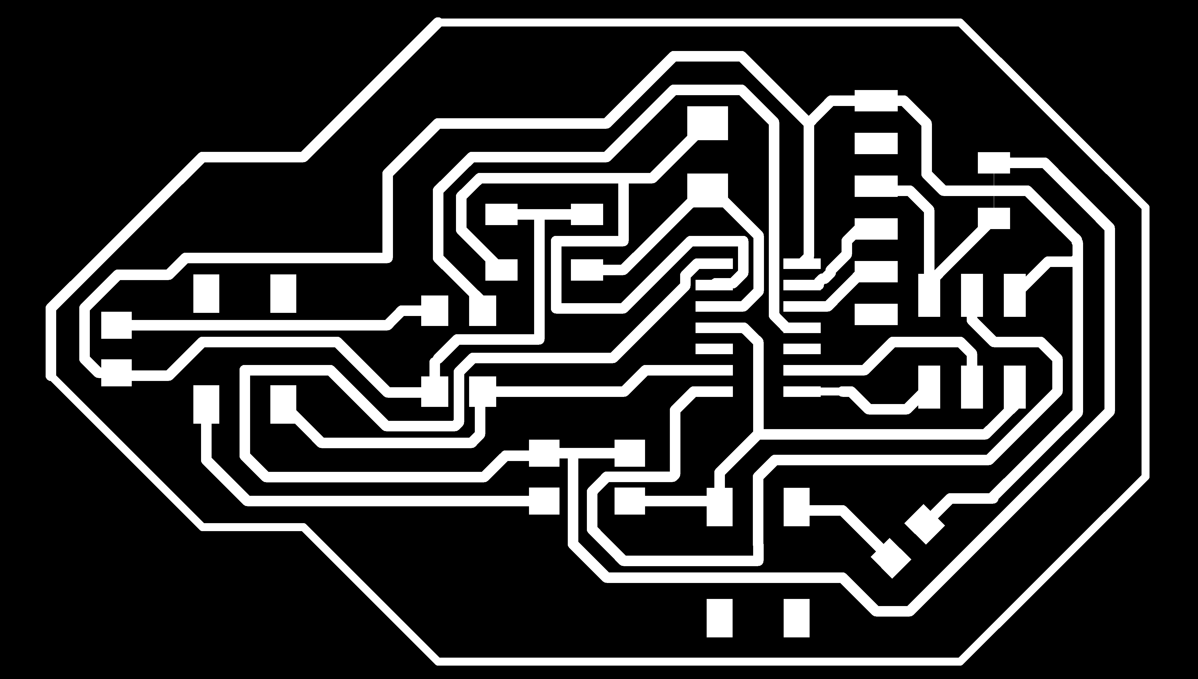
Afterwards, We hide the layers except the top layer (the one that has the routes in it) from the layers option:
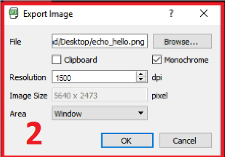
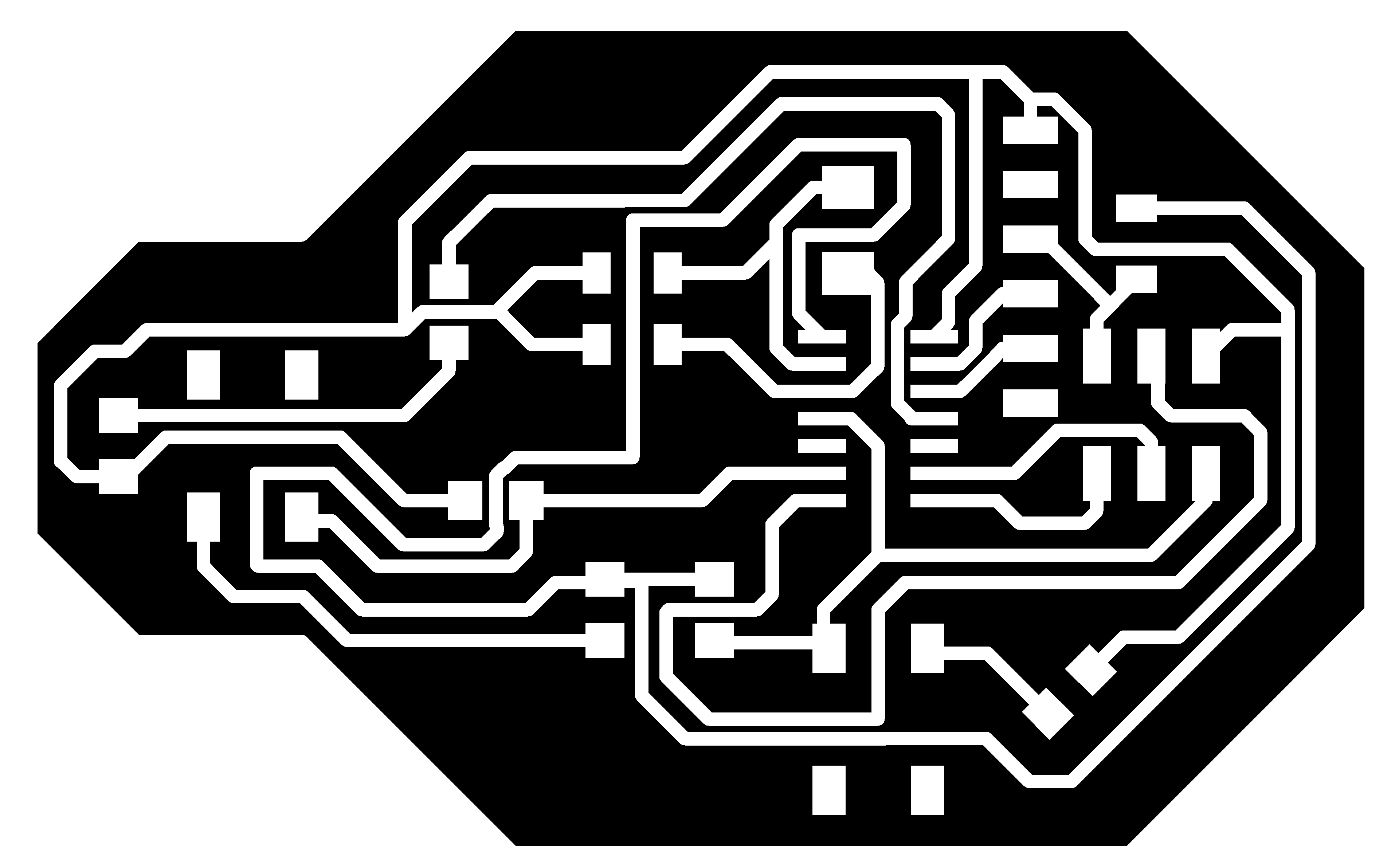
Then we export the result as an image and we check the monochrome box to make the picture in black and white, and select the resolution to 1500px.
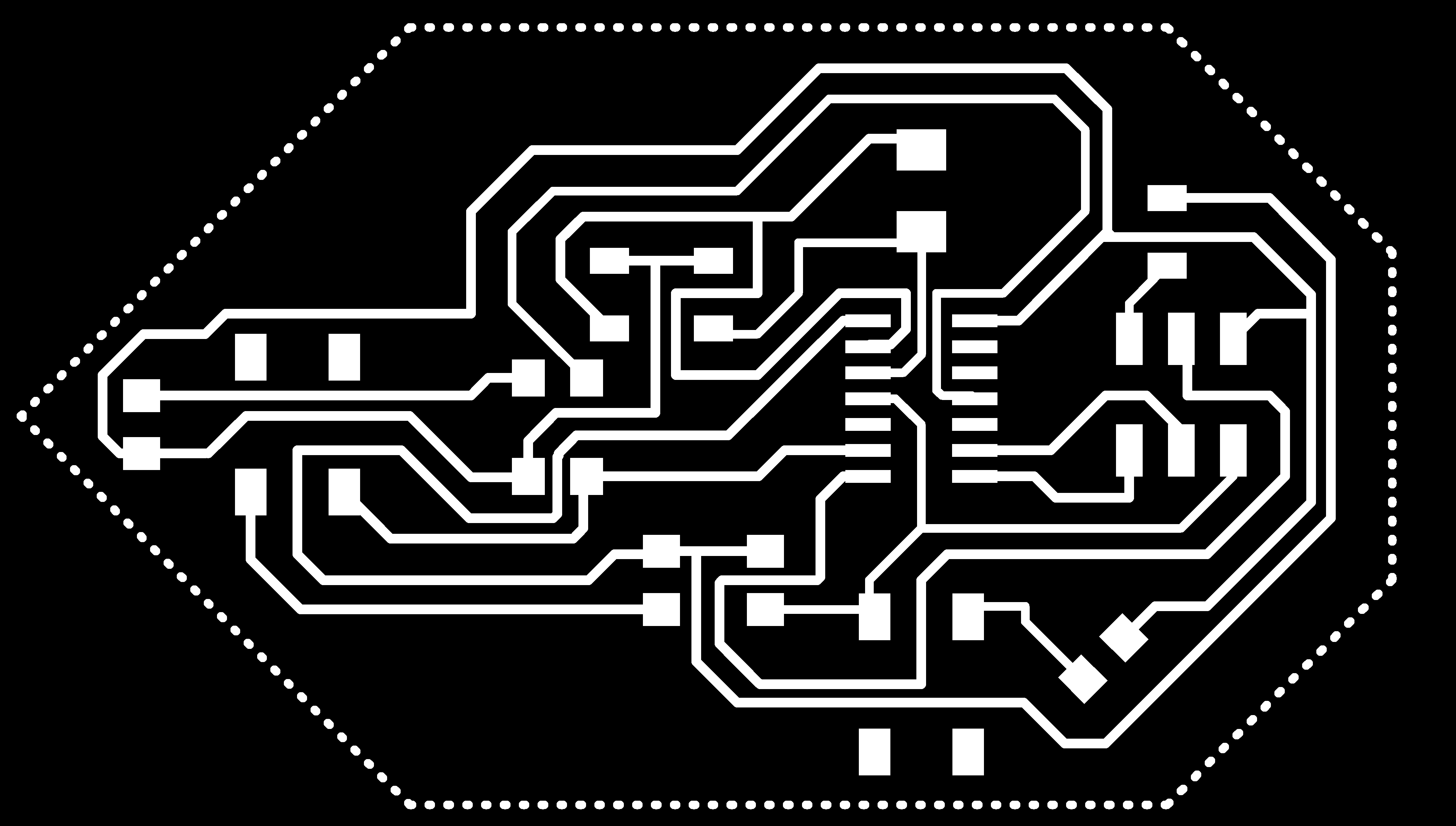
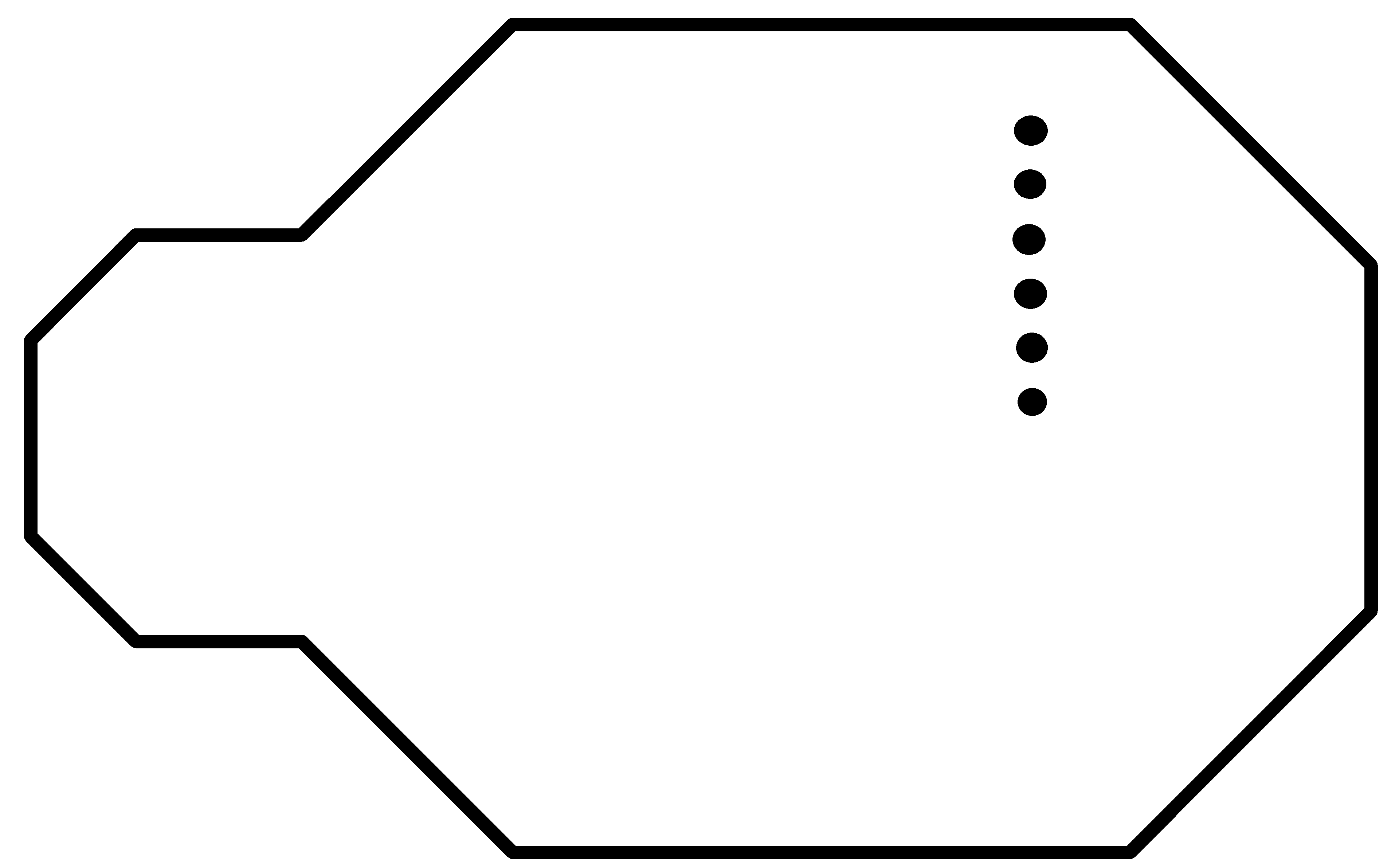
the result image would look like this:
then we continue the process just like we did in the Electronic Production week.
Obstacle: In milling the board, there was a problem that the lines would either misappear for how thin they are, or make a shirt circuit because of the small clearence between them. so I had to adjust the design and thicken the lines and clearence:
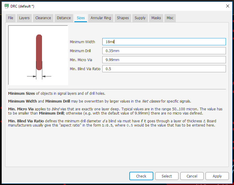
the new result was succesfully turned into a board
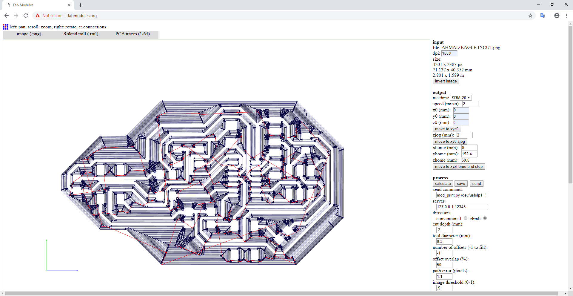
on th fabmodules, i used a -1 offset to make the soldering easier.
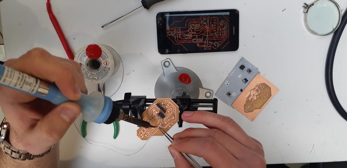
step 2: Milling and soldering the board, just like we've done in the Electronics Production week.
Now to the programing stage!
The first thing I did was to write the Arduino code; a simple code to control the system that if i push the button the LED will light up, and will turn of when I raise my finger.
But in order to write the aformentioned code, I had to find out which pin has which number. I found this figure on google that demonstrates the name of each pin:
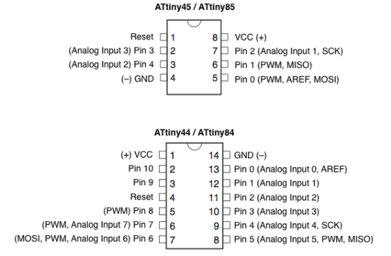
Trakign the lines on my board, we can see that I am using pin No.7 for the button and pin No.2 for the LED.
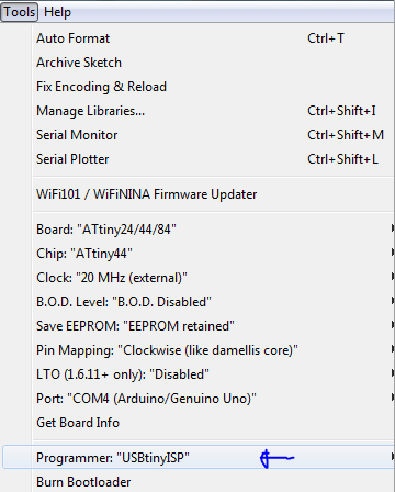
Before running the code, we have to connect the Arduino board to the attiny and configure the Arduino as an ISP for programming.
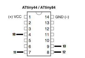
Following this sketch helps with connecting the Arduino Uno board to Attin44:
To program the Attiny we have, we need to download the following Attiny files.
Unzip the attiny zip file. It should contain an “attiny-ide.1.0.x” folder that contains an “attiny” folder. Locate your Arduino sketchbook folder (you can find its location in the preferences dialog in the Arduino software) Create a new sub-folder called “hardware” in the sketchbook folder, if it doesn’t exist already. Copy the “attiny” folder (not the containing attiny-1.0.x folder) from the unzipped Attiny.zip to the “hardware” folder. You should end up with folder structure like Documents > Arduino > hardware > attiny that contains the file boards.txt and another folder called variants.
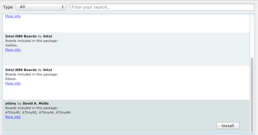
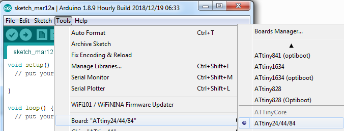
After doing that, go to Tools>Board>Boards Manager. And there you should find an Attiny section. Click Install.
After doing so, select the attiny board then select the other slots as shown:
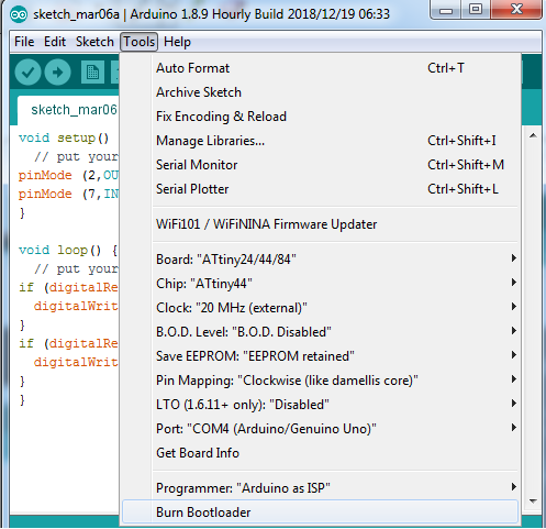
Notice that the crystal chosed was the same as the one used in the board (20MHz). And for the programmer, we select Arduino As ISP. Then we click Burn Bootloader.
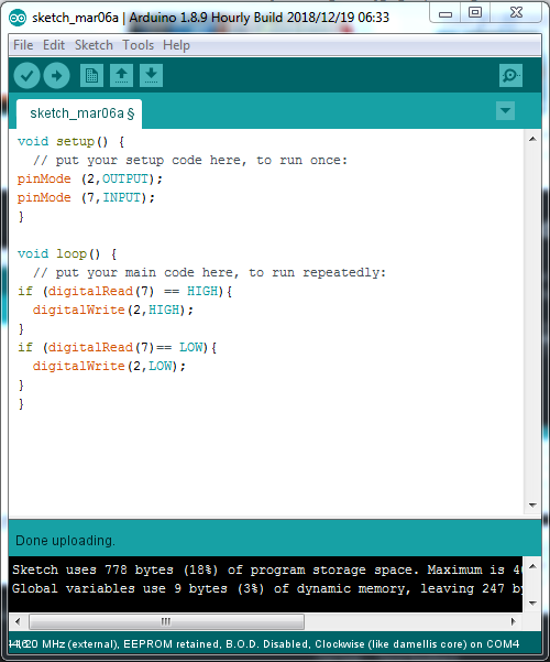
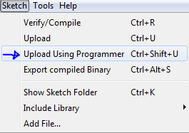
Finally, we upload the code by going to Sketch>Upload Using Programmer.
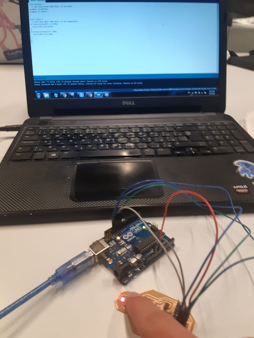
And like that, I have a functioning board.
Programming using FabISP
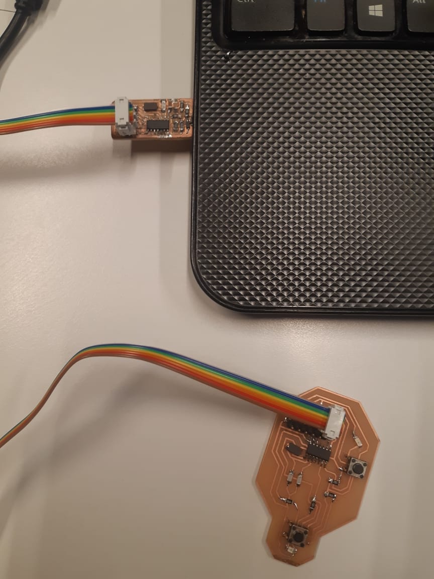
First of all, I had to configure the ISP so it could be read by the computer. I followed the instructions given by FabLab tutorial. then following almost the same steps as in programming using Arduino Uno. My Arduino software could read the ISP and give it as an option for programming. But after running the code, and even though it gives Done uploading, the PCB still wont work. This problem shall be searched further in the Embedded Programming Week.
files
