Week no.4
- Electronics Production
- In-system programming (ISP)
Assigments :
- Make an ISP Board by milling the PCB
- Should work as a programmer to upload software to another board.
PCB fabrication - FABISP
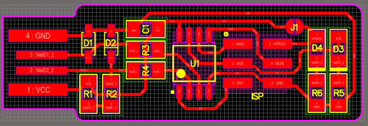
For this week assignment, I started looking at the ISP documentation, understanding the model board schematics and PCB design. Our group choose to build the FabTinyISP and the first task was to go through the tutorial.
This is a minimalistic version of an ISP, no reset switch, no crystal onboard, the control frequency works in a ingenious way by using the host CPU to generate the ideal clock frequency for a reliable USB communication. The tutorial is well documented from milling to programming, an enjoyable learning experience.
For me, the greatest learn was my first experience with FabModules. It´s an interface that runs on your web-browser witch can handle Image processing, Machine specs configuration and G-Code generation, pretty impressive !
First goal : milling the PCB
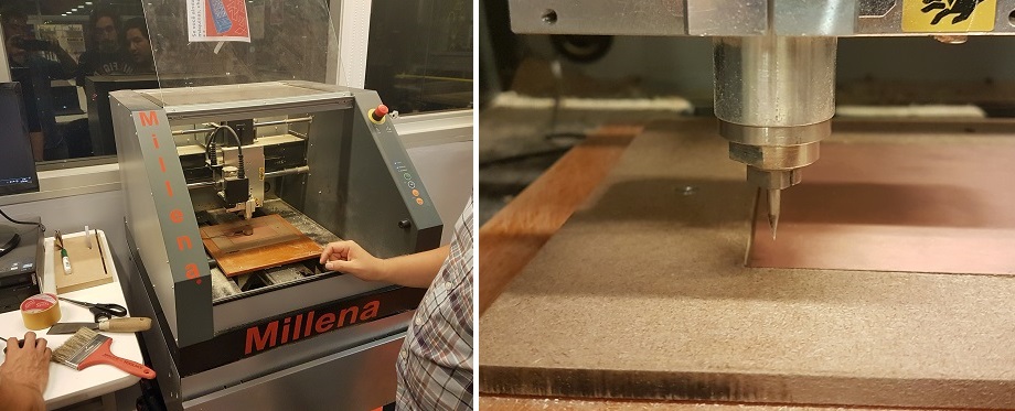
I´ve managed mill the circuit board from a png schematics using FabModules. By just uploading the image and providing the milling parameters (tool configuration, offset, path, cut depth) the application can generate the G-Code for our exactly Machine - Roland MDX-40.
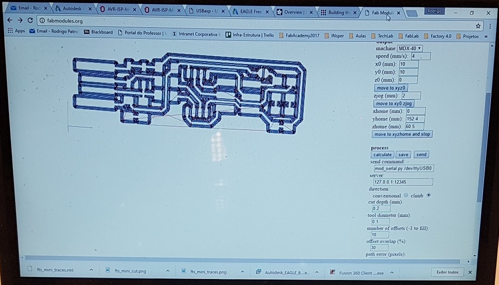
The Fabmodules parameters I used for milling were:
- Imput Format : image PNG (hello traces.png) 1500dpi
- Output Machine : MDX-40
- Speed : 4mm/s
- Cut depht : 0.2mm
- Tool diameter : 0.1mm (V cutter mill 30º at 0.2mm depth)
- Number of offsets : 8
- Offset overlap: 40%
- Calculate path
The photo of me filling the forms of FabModules can be zoomed with a click to better se the parameters.
Below that picture is a close in the V carve cutter tool we used, this is not a common tool for milling circuit boards. I have already made some boards on our milling machine (kindly called Millena) but usually with a top mill, but we went short of milling bits at the time. So we tested a V shaped bit to machine the board.
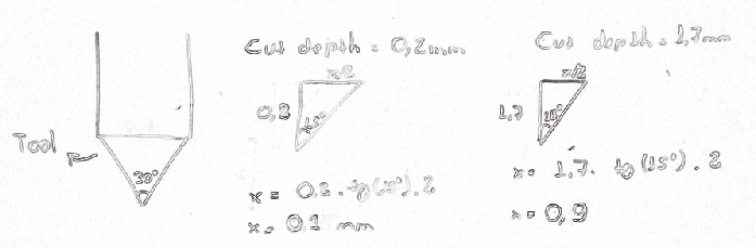
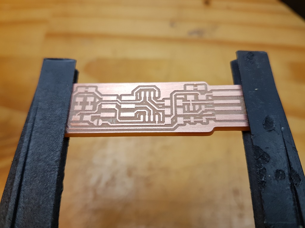
The resulting job was most surprising! Besides its trapezoidal shape, the milling worked quite well. The only detail was to carefully set up the Cut Depht parameter, for that we used trigonometry to calculate the width from the point at 0.2mm high with a 30º angle.
Also adjust the overlap and increase the number of offsets, the machining took more time than usual, but the results were good ! Also adjust the overlap and increase the number of offsets, the machining took more time than usual, but the results were good! Also revealed to be an interesting tool if you want to make an all-in-one process for milling and cutting the outline border.
I found a interesting tutorial that coverss the basics of CNC bits HERE.There is a picture of the finished board on the slideshow below.
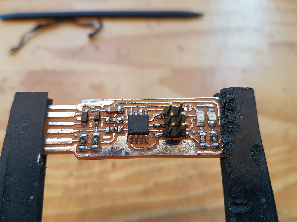
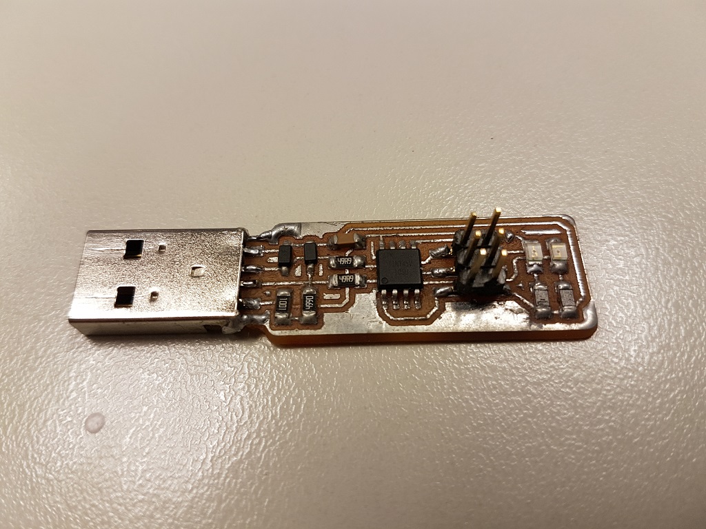
Second goal : soldering the components on PCB
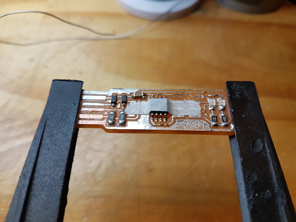
Started soldering from the big and more complex components to the little ones, also used a stick tape to help align the processor pins to the soldering pads. Used some soldering paste to help distribute heat and spread the tin, also covered any unprotected cooper to protect against oxidation since I didn´t make any cover.
After soldering, I notice that the USB made directly on the board had not the ideal size. So I upgraded : cutted and soldered a connector recycled from a dead Pen drive. A final contact test with the multimeter and result worked really nice !
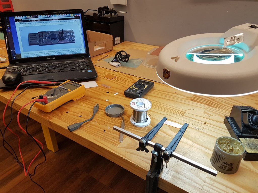
Thirty goal : programming
I burned my ISP proggramer in a PC running Linux command prompt, so I didn´t capture the screen log. The process was petty straigthfoward.
- sudo apt install avrdude gcc-avr avr-libc make (software update)
- Downloaded and extraccted the firmware fts_firmware.hex
- ATiny45 using PROGRAMMER = usbtiny
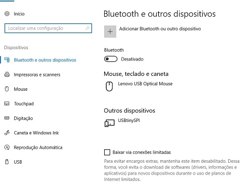
- Connect to USB port and run MAKE FLASH
- Tested back on my Windows computer if it recognizes, ok!
- MAKE FUSES - disable reset pin to allow programming
- Fuses ok ! (H:FF E:DF L:62)
- Success !! Last Step was to remove the solder jumper
- All set !!