Electronics design
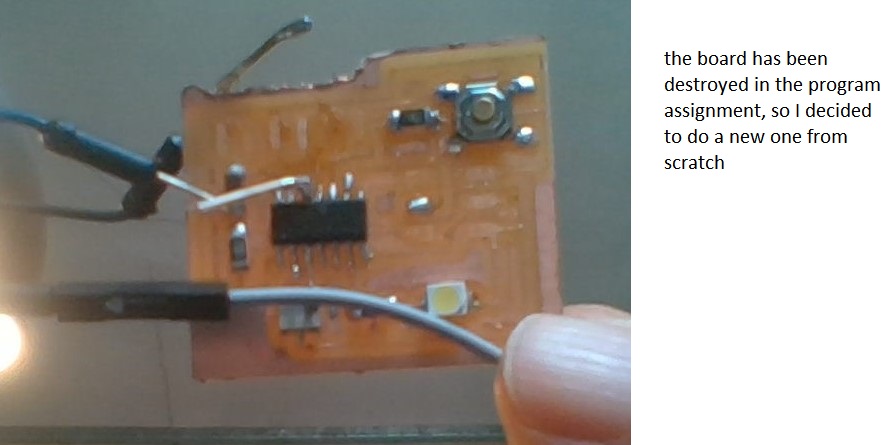
individual assignment : Redraw the echo hello-world board, add (at least) a button and LED (with current-limiting resistor), check the design rules, make it, test it.
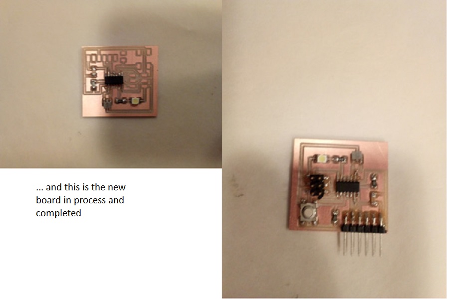
.JPG)
.JPG)
to learn how to select a resistor mode I have gone to the following sources
pull up resistorsresistors sparkfun
They operate using the same concepts, except the pull-up resistor is connected to the high voltage (this is usually 3.3V or 5V and is often refereed to as VCC) and the pull-down resistor is connected to ground.
as the assignment said we should add Resistor (value 10k) pull-up resistor.
.JPG)
.JPG)
.JPG)
.JPG)
.JPG)
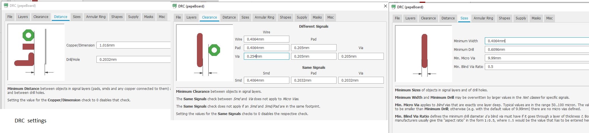
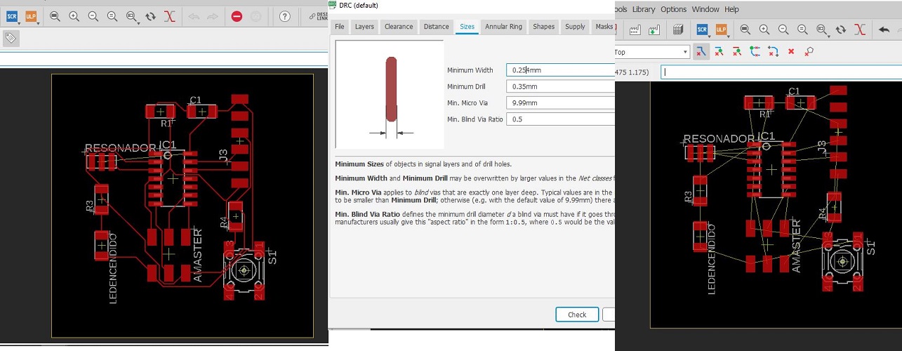
those are the DRC settings used here.
some of these settings were not the best, and I was mofifying them in later boards.
An important factor to consider what is the width of the copper tracks. It is very important to modify the configuration of the eagle DRC so that the width of those days is never less than 0.4 millimeters. Below that width the copper tracks become very fragile and their manipulation can be broken at the same moment of the milling. On the other hand, a track smaller than 0.4 mm, according to experience, easily will disappear or take off in the component soldier.
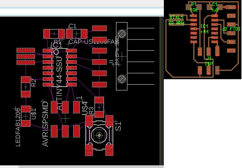
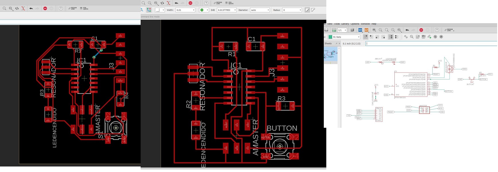
this is the disposition of elements based in some other examples and the Neil`s example
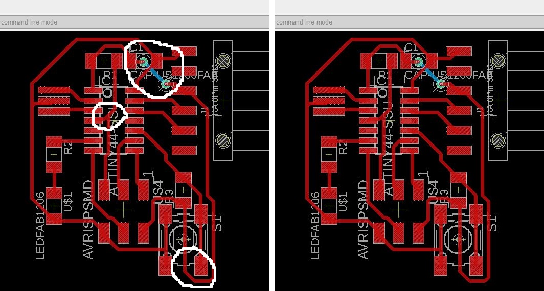
With the execution of auto router you get a very acceptable route layout and of course an excellent starting point to have a first idea of how to establish the tracks. In the first analysis of auto router it is very common to have lines that intersect
where auto router gives the option to establish a line on the other side of the board. Since we want to avoid this by supposing a complication we estimate other solutions made by hand.
But you also have to be careful with other routes
that auto router gives for good.
We must avoid Having very close to the traces of the elements, ie the separation set in the DRC.
Keep in mind that diagonally traced paths near a footprint often give problems in the corners when
we run the path in fab modules.
You have to be especially careful with the tracks below the attinny processor and make sure there are no strange connections or too close to the tracks.
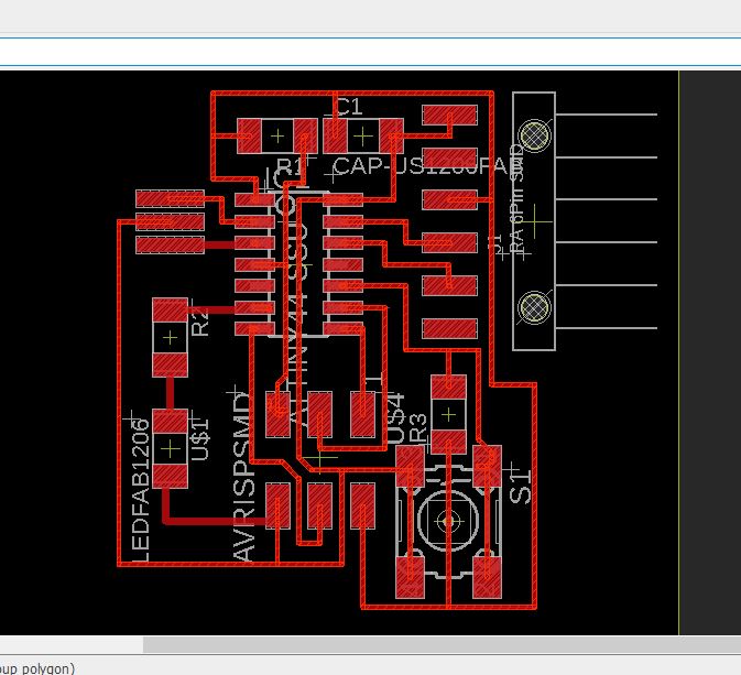
At this moment with very little experience about routing on a board this is the final traces for lines
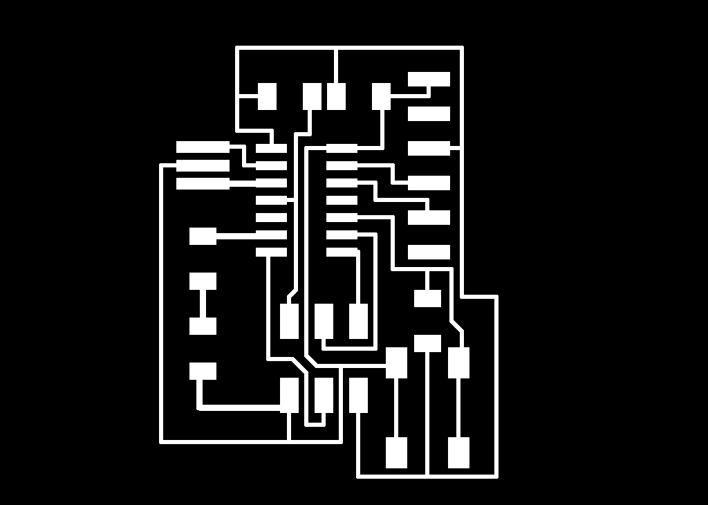
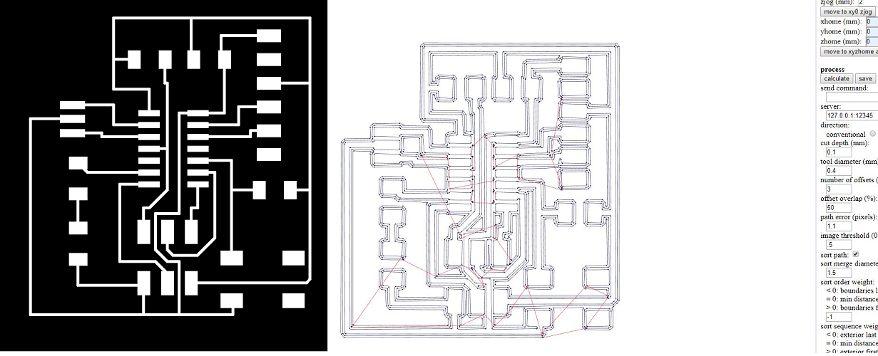
UPDATE: generating the png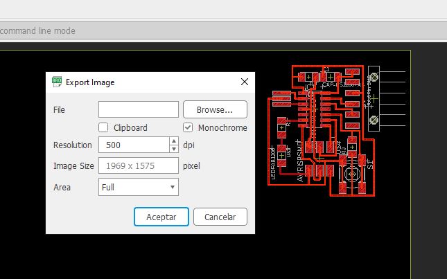
eagle can export as png the plate diagram for use in fab modules.
for this go to file / export / image.
select where to save the png
use a resolution of no less than 500px
select the monochrome box
soldering process
.jpg)
.jpg)
reconstruction
UPDATE : EAGLE CONSIDERATIONS
EAGLE is a software designed for the design of printed circuit boards (PCBs) that, historically, has played a very important role in the circle maker / hacker for being one of the first options with limited free licenses. Without going any further,
the Arduino design files are published in its format and, in addition, is one of the few options in the world of electronic design automation with support for Linux.
It is a good software with multiple facilities for the design of PCBs,
it is multiplatform and has a good community of users behind that release a large number of projects to use or study them.
EAGLE Provides a large number of tools for circuit design. All of them are well structured according to the workflow
separated between the types of connections and the final mode in which the board is executed.
Among them, it is worth mentioning a very useful tool that is an auto router that allows a first design of the circuit tracks.
But it also
allows libraries of elements that can be imported that transfer to the board the footprints already dimensioned of all the elements.
Multiple functions in its different menus on track layout, copy of elements, transfers and turns, different
layers very useful when selecting elements, and a group of tools to establish labels with characteristics that are of great help in the final design of the board
UPDATE : SOME OTHER SOFTWARES KIKAD
kikadThis electronic design software is basically composed of an electronic schematic editor, a PCB editor, a component-footprint associations editor (for the PCB design) and a file viewer. Everything is centralized under the same interface, from which
opening the project file you can access all parts of the project (capture, PCB, etc ... ..)
The capture process, with this tool is comfortable and quite easy. There is not much to tell here. The menus are intuitive and quite comfortable.
For the selection of fingerprints in the PCB manufacturing process, another application is launched that allows us to look for component by component, the most appropriate footprint for our needs.
At the time of the creation of the PCB,
it also has an autorouter
The algorithm generates a pretty good routing, just like in eagle being able to specify the minimum space between tracks (clearance). It will always be necessary to review the PCB by hand and modify some clue,
something inevitable
In conclusion, kicad has seemed a good tool for capturing schemes and design of PCBs, very similar to eagle although for my knowledge of electronics and the term surely I have not got more than a superficial knowledge
UPDATE : SOME OTHER SOFTWARES
here is some other software I found in electronics design
PCBWeb designerzenith
tinycad
osmond
express pcb
geda
UPDATE: EAGLE KICAD COMPARATION
Price
kiCad is a free and open source software created by a community of users. You can download its source code and modify it.
eagle is autodesk property, but can also be downloaded for free.
User interface
In user interface both software are very similar.
However, Kicad has a set of keyboard shortcuts to perform common tasks such as rotating a component or drawing a cable. eagle has a line of nodes where you can write program commands
directly.
For libraries, both contain methods to access the library of elements with their footprint, and both also allow designing their own elements.
The libraries in Eagle have both the elements and their footprints while in kiCad
the symbols and footprints are separated into different libraries.
While in eagle to design a board, it is enough to design the schematic and its connections and then generate board for the necessary corrections, in kiCad the
fingerprints of the components are chosen at the end.
kiCad also incorporates 3D viewer and you can see all the designs and their components in three dimensions, which makes it easy to understand and size and space as well as the
provisions of the components.
For all these reasons, eagle seems more friendly to those who are starting to design boards.
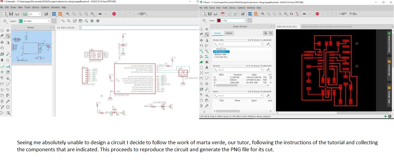
local instructor marta verde
tutorials autodesk
tutorials sparkfun
Download
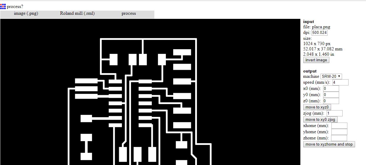
if you find some documentation failures in the board manufacturing process please go for a complete process to the assignment 11 "output new board "
see complete process output board