Electronics design
Assignments
#1 - Redraw the echo hello-world board, add (at least) a button and LED (with current-limiting resistor) check the design rules, make it, and test it. Extra credit: simulate its operation. Extra credit: render it
This week, there is no pre-cooked materials such as for week 5, where everything was prepared for us: the schematic, the pcb, the firmware, .. This week, we have a example of a schematic based on the ATTIny44 and we have to add components, to route the PCB, to mill it, to put all the components on it and to make a "hello board" proof of concept.
References
Lecture
This week is about electronic design:
- What electronic design tools 3D should I use ?
- How to scan get started with KiCad ?
- How to create a schematic using KiCad ?
- How to create a PCB once my schematic is ready ?
- How to mill the pcb and install the components on it
- How to build , flash and test the software once my pcb is ready ?
Recitation
Discovering tools that have been developped or discovered over the time by and for Fab Labs
Topics covered (course) Video recording (course) Video recording (recitation) Students and Labs My filesLearnings
Choosing a tool for electronic design
There are multiple tools and it is sometimes hard to figure out which one fits our needs the best: EAGLE, Multisim, EasyEDA, Altium design, OrCAD, and KiCAD. I found this site for those interested in a comparaison between those tools. For my Fab Academy journey, I decided to try KiCad, mainly because it runs on Linux and there is no issue with licencing or any kind of subscription
KiCAD is divided in five parts:
- Project manager
- Eeschema that is the schematic capture editor. Eeschema has features like custom symbol creation, electrical rule checking and hierarchical schematic sheets
- pcbnew: shows layout of PCB in both 2D and 3D. It provides very easy way to routing the components and also it makes easy to troubleshooting of PCB. if you want to change any vias, hole, trace or any other components of PCB, it is easy in KiCAD compared to other software
- gerbfile: used to generate Gerber file
- bitmap2component: can convert images to footprint.
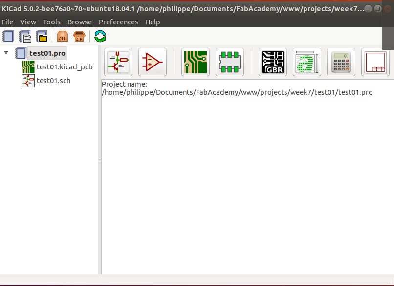
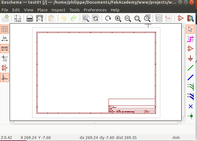
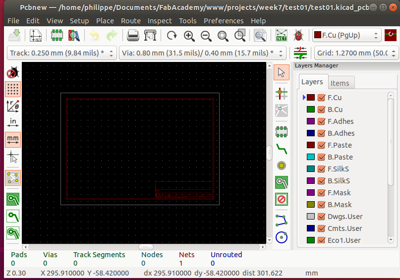
Overall software is good for beginners and biggest advantage is that, this software is free available. So, one does not require to purchase any licence or not require to find cracked version of it.
Getting started with KiCad
I followed this tutorialand this one as well. There are many tutorials but pay attention to the Kicad version (the one I am using is 5.0.2), there are major changes between versions and a tutorial becomes quickly obsolete
The first step is to setup your environment: I found out some Fab Lab libraries here and I installed them. There are two libraries: one for componennts (fab.lib = logical entities) and another with component footprints (fab.pretty = a set of modes = physical entities).
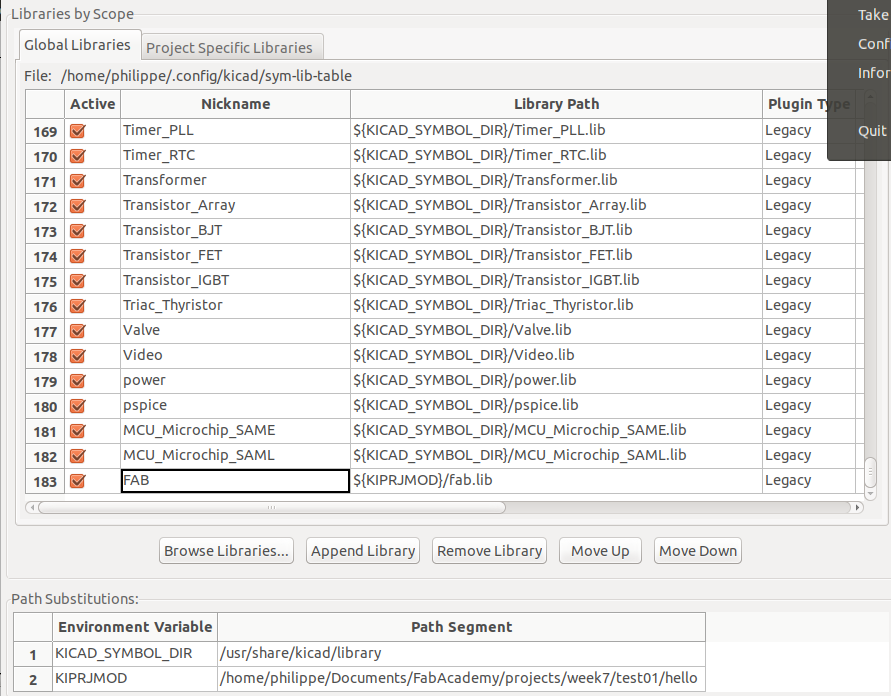
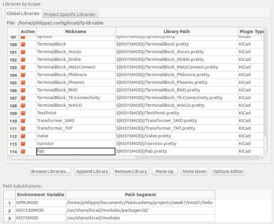
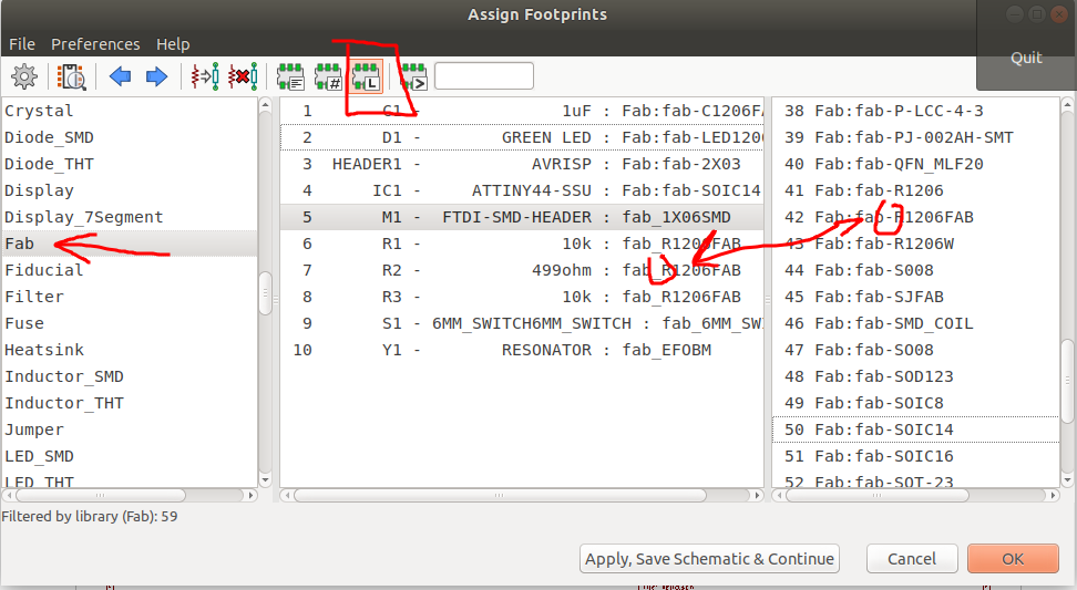
Note: for second one, I think there is an error in file naming convention that prevents Kicad for matching the logical components with the physical components automatically ("-" vs "_" in file names)
Creating a schematic with KiCad
I followed this tutorial
As a starting point, I checked what other students did last year (like Catherine Blanchard (she's using Eagle it does not change anything regarding the schematic and pcb routing outputs
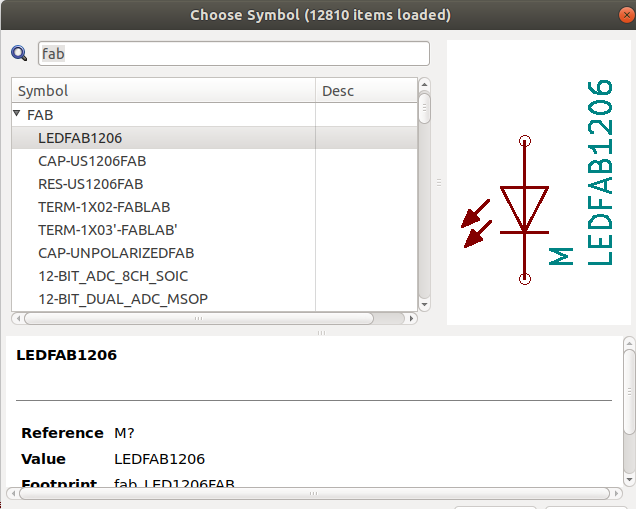
To add each component one by one, press A and then pick the right one in Fab Lab libray
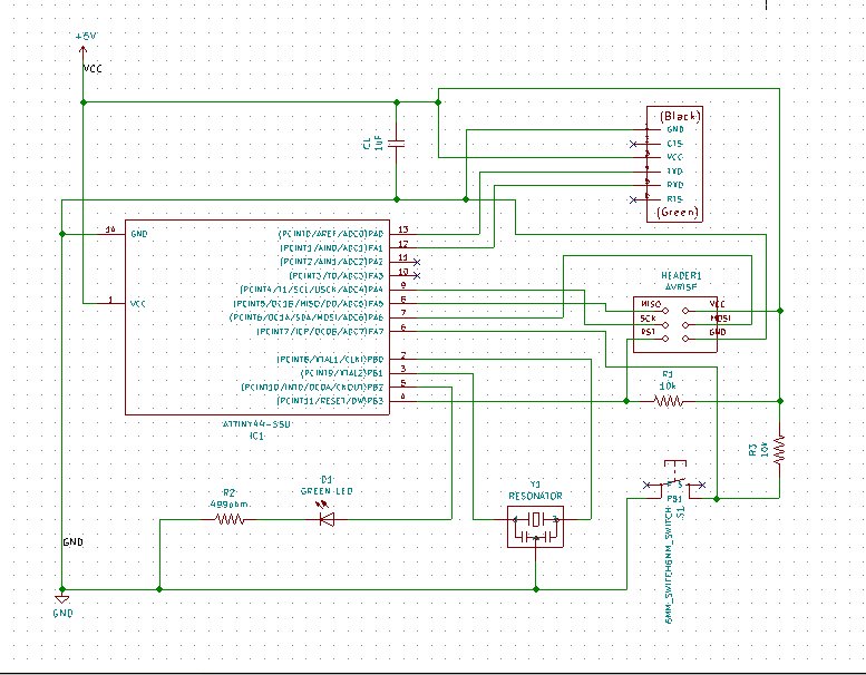
Then place them in a logical way, set values and annotations and wire them together (see the tutorial for a step by step guide on this)
Note: here are some usefull keyboard shortcuts:
- a - add component
- c - copy a component when the cursor is over another component
- w - wire component
- v - edit component value
- Esc - escape mode or whatever command in progress and return to normal pointer mode
- ctrl+s - save.
Do not forget to run the ERC (electrical rules check). I had the following errors to fix (all errors are displayed on the schematic using green arrows):
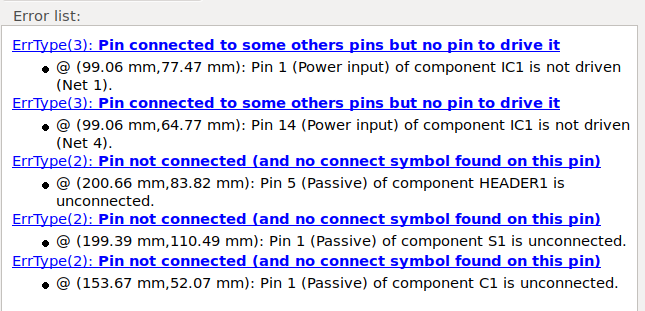
Let's check them one by one (not in the order listed above)
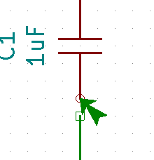
Simple fix... add some lenght to the wire so it can reach the component
The second one is weird. Connection is ok but ERC does not like it
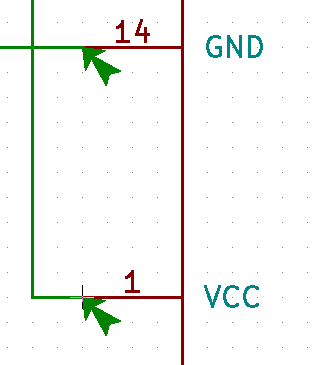
I did not fix it, it looks, according to the my readings and searches, that the issue is related to the pin definition on the component (MCU) level. A pin has to be declared either as an input, output or bidirectionnal. For VCC and GND, it is not that much applicable
The third one was obvious : my reset line was not connected
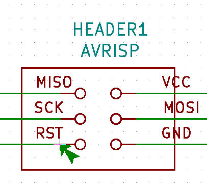
I fixed it.
The last one was less obvious : on the small switch, there are 4 legs but we use only two.
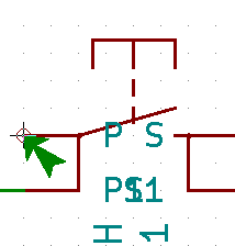
I fixed it. I had to put "no connection" flags on the one that are not used. Note that I changed my mind later when I realized I could use that as a solution to make a trace jump over another (same concept as when you put 0 Ohm resistor on a PCB
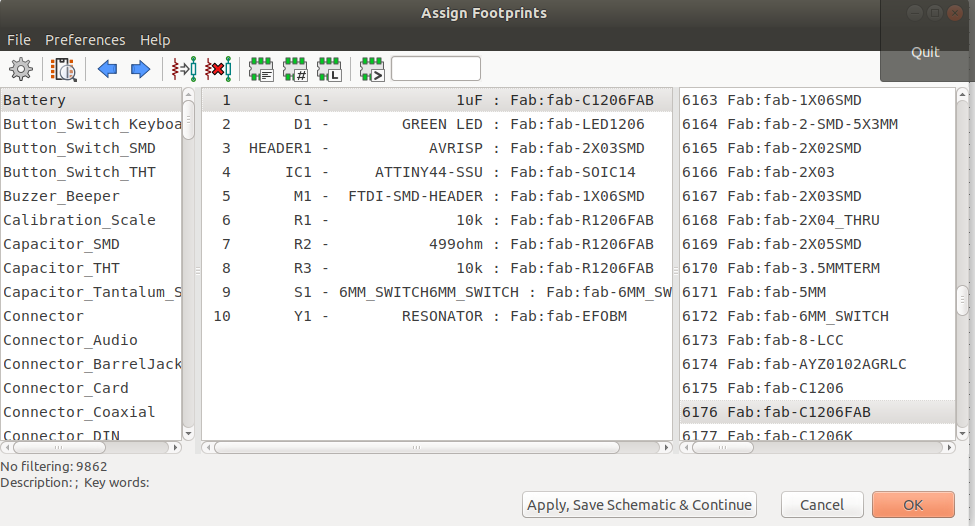
The next step is to associate footprints to logical components, i.e to help the PCB designer we will use soon to figure out how a given logical component looks like from a physical point of view
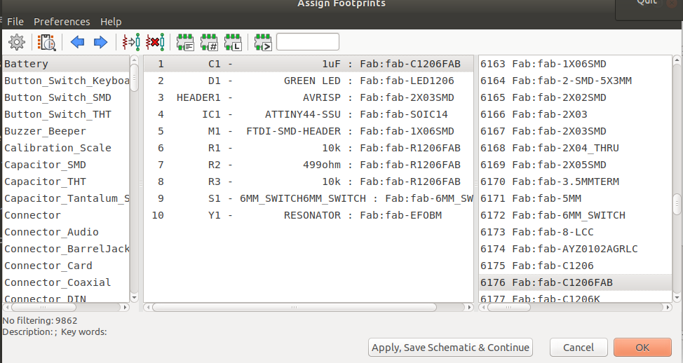
Note: I made a mistake here and you will see later how I recovered from it. The mistake was related to the resonator footprint. I took a component but not the right one and the footprint was not correct (3 legs but the real one has only two and the pads are not well sized neither). I should have taken this one:

Once everyting looks good, the next step is to export the "net list" ( a "net' is a physical connection between one or may components) in order to make it available for the PCB design SW
Creating a pcb with KiCad
I followed this tutorial
The PCB designer is another program you can start from the main view. Once started, the first step is to import your "net list"
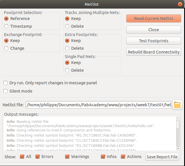
The result is a messy PCB... it looks there is more work to come !
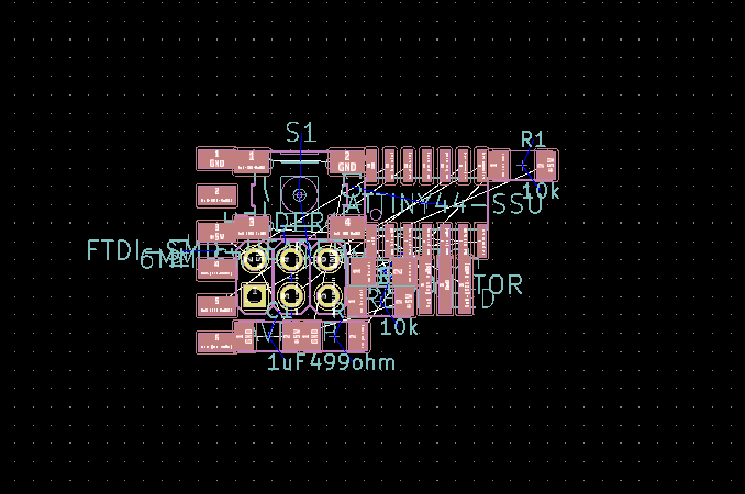
With the new tool comes a new set of keyboard shortcuts:
- + - switch to next layer
- - - switch to previous layer
- m - move item.
- b - update ground polygon pours
- Del - remove a trace or component.
- x - route new track
- v - add through via
- Page Up - return to the top copper layer
- Esc - escape mode or whatever command in progress and return to normal pointer mode
- ctrl+s - save
This is the first draft
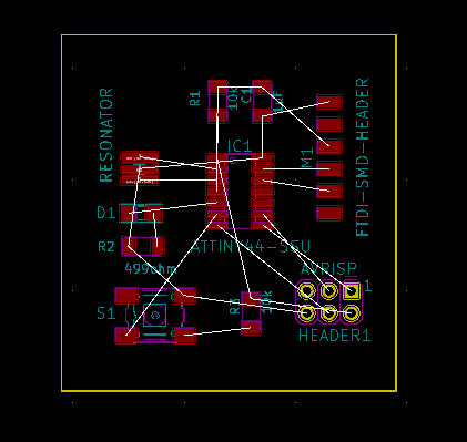
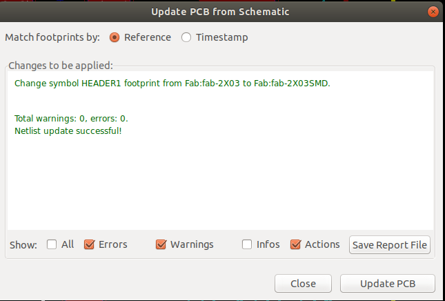
As you may notice, one of the component looks different. I made a mistake when selecting the 2by3 header footprint. I took the throughole version instead of the SMD one. I've to go back to the schematic, to update the component footprint, export the net list again and come back to PCB designer and re-sync with the net list.
The next step is just like meditating... You have to figure out a way to create physical connections but.. without any trace crossing another trace. There are tricks, like..
- taking the long road to go around a component
- go under an existing component that is large enough (for example an SMD 1206 resistor)
- adding 0 oHm resistors to create artificial bridges
- adding "via" to jump to to other side of the board or even another layer between n boards (but then it becomes more complex to mill)
I mentionend earlier the concept of "net" and here is an example of one of the nets: the "VCC net" that brings power whereever it is required
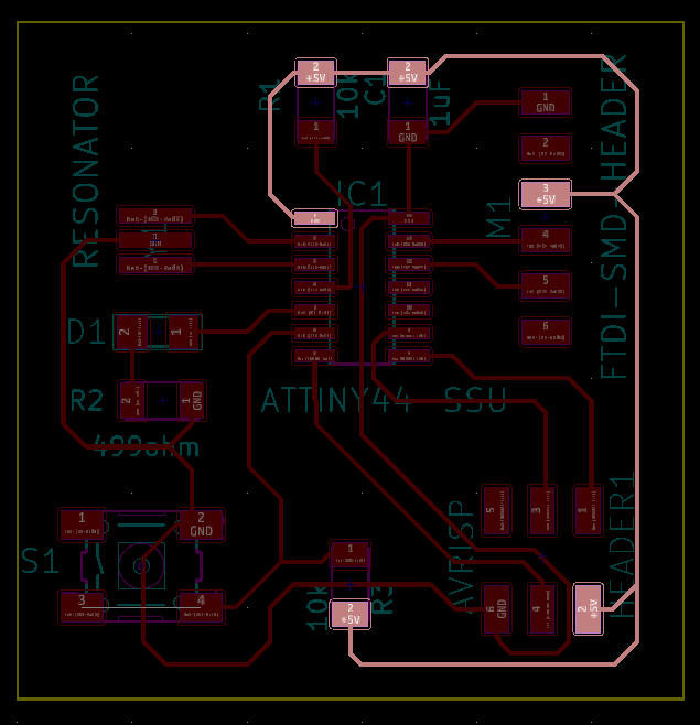
And another net representing the GND
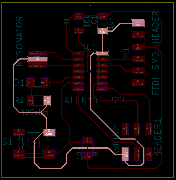
But there is another approach for this one: to build a "ground plane". It means to consider every peace of non connected copper to be part of a big net, this one connected to the GND. And here is how it looks like at the end
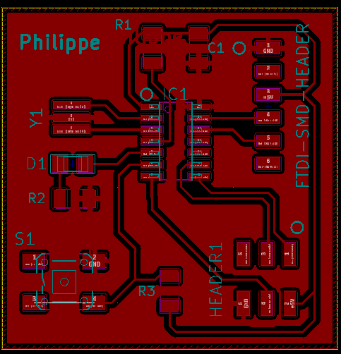
The next step is to go through another set of checks: the DRC checks. The idea is to verify whether your nice hand-routed piece of art could survive to real world, with milling constraints and with some physical reality related to electricity theory I don't want to explain here (I would not be able anyway !). Note: the default value for trace width is 0.2 mm.
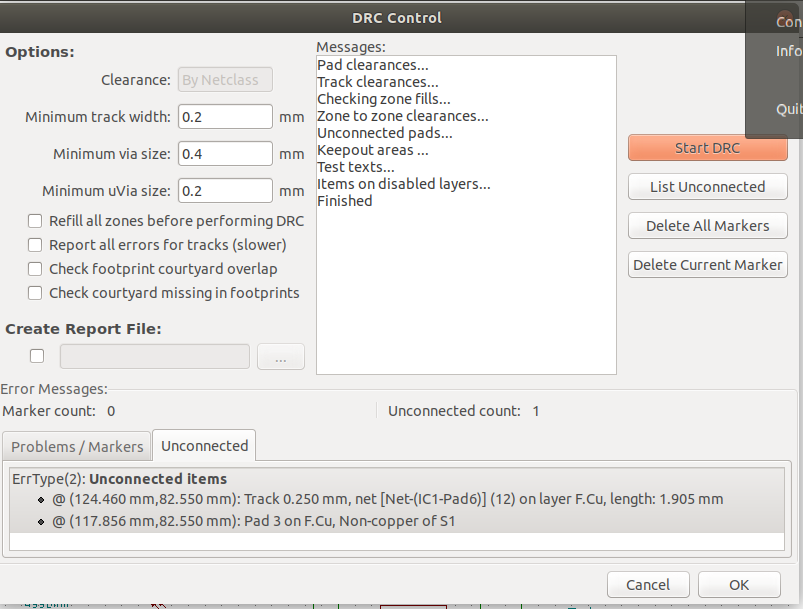
ERC check found out some errors related to unconnected items and I fixed them.
The last step is to export SVG files (this is specific to our milling process. With PCB manufactured online with diffrent process, I would probably have to export Gerber files)
Milling the PCB and placing the components
This is similar to what we achieved in week #5 and there is no use in repeating the documentation. I still want to take some time to enumerate what went wrong. The first attempt was the following one
I missed an important step: to invert the picture ! The result was a nice but totaly useless piece of copper.
The next attempt was not good neither
I missed a parameter (offset). I will not trust the tools and I will check the RML files manually before sending them to the machine, starting from now !
The next attempt was not that bad but I realized the traces were very small (compared to the "Brian" project I repeated two week ago. I tuned the design rules to get a better output

IO finally got it... Here it is !
Soldering time
A few things to mention here:
- First, the "ground place idea" looks good but it is harder to keep it clean when soldering. I should be more carefull with flux, I should not put flux on the ground plane areas, It will work, but it looks messy.
- Furthermore, I found an error with the resonator (3 legs vs 2 legs) but I also found a way to go over it, thanks to a piece of the ground plane. I isolated to part located on the top by cutting the trace and I used it as a pad, connected to the right pin using a small piece of wire. Ok, that is definitely an "pre-alpha" board but it should fly... and help to find other issues BEFORE a new revision
Cleanup time (using 99% isopropanol) ..
Testing time
The obvious test is a VCC tot GND continuity test, which should normally conclude there is .. no connectivity (i.e no short). Done !
I wanted to push more on testing and and I decided to go ahead with voltage test.. 4.89 volts.. it makes sense
And then a current test, just to figure out how much current goes through that circuit. Answer is 11.91 mA. My PC will not complain.
Flashing the firmware
This is similar but not identical to what we achieved in week #5 and there is no use in repeating the documentation. There are 3 steps: build, set fuses and flash
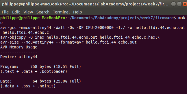
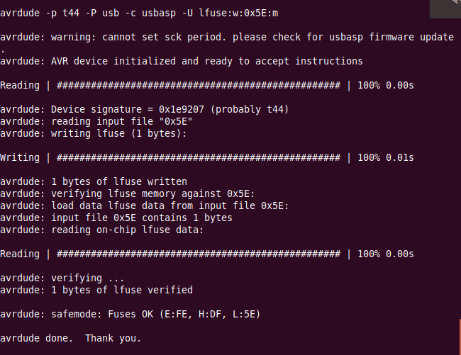
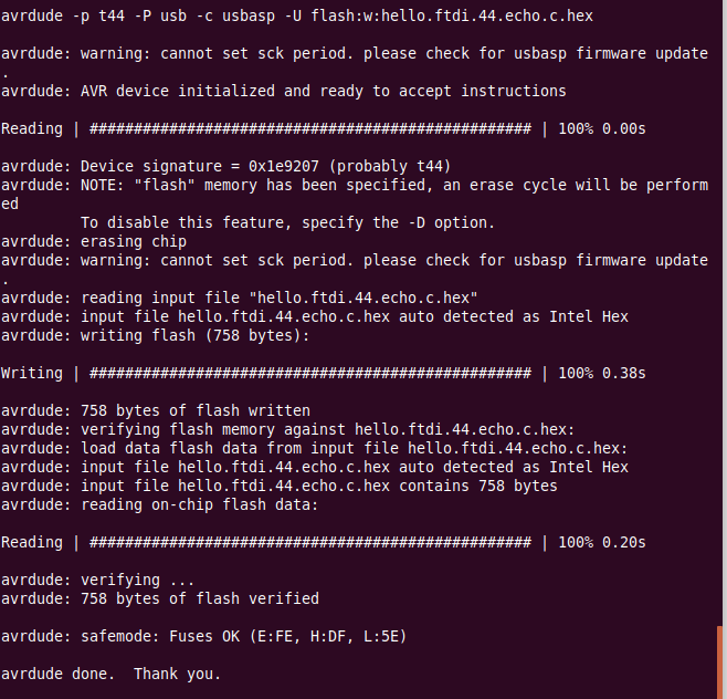
Let's connect the FTDI cable and see how the PC manage it..

By the way... what is FTDI ??? FTDI is known as an acronym but it is in fact a company name (founded in 1993). Those who were born before 1993 probably remember the old serial port and its connector (for the others, note this is NOT a plain old VGA connector)

On such a connector, two pins are dedicated to data transmission (Tx and Rx). Information is transmitted one bit a a time.
Modern computers without serial ports may require USB-to-serial converters to allow compatibility with RS-232 serial devices. Serial ports are still used in applications such as industrial automation systems, scientific instruments, point of sale systems and some industrial and consumer products. You cannot just cut a USB cable and crimp each wire, you need an MCU to convert the signal and a software driver to talk to it.
Let's start a serial console (I used the Arduino IDE one).. According to the source code of the firmware, the MCU should echo back any typed character
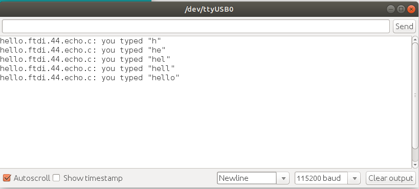
From a test point of view, we know current and voltage are ok but.. what about the communication with the PC (over a FTDI cable). Is there a way to visualize it ?
A few year ago, I bought a small USB oscilloscope on a Kickstart campaign. Here is how it looks like
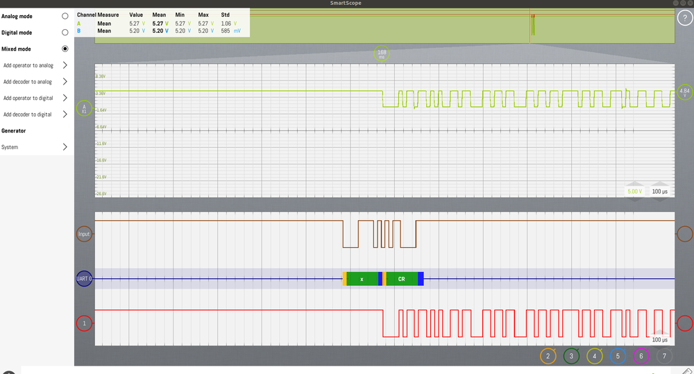
On the front side, there are two probes and on the back side there are connection for digital signals (IN and OUT (generator). Here is how to connect it to analyze Tx and Rx signals between the PC and the MCU
And when I type an "x" on the terminal, here is what is display on the Smartscope App. The signal on the top is the analogic version of the communication sent by the MCU to the PC, measured by a probe. The second one, on the bottom is a numeric view on the signal sent by the PC to the MCU, analyzed by a decoder and displayed in a human readable format on the third line. The last line is another numeric view from the signal sent back from the MCU
Achievements
Use KiCad to design a schematic, derive a pcb and then mill it on the SRM-20
Done. I will build another board revision in two weeks, with an updated design with all identified fixes. I'm still building my DYI reflow oven and I would like to use it to reflow the components on the new board
Use the test equipment in your lab to observe the operation of a microcontroller circuit board
I mainly used a multimeter to check if there is any short (conductivity test), to measure voltage and to measure current as well.
Using the Lab Nation USB osciloscope
I wanted to learn more about osciloscope but the entry price was to high. Then I discovered this USB smartscope. This is more than a conventional osciloscope
Capstone
Design time !
I started thinking about the components I will use and how they will be placed on a schematic