Electronics production
Assignments
#1 - Make an in-circuit programmer by milling the PCB, check if you can program it, then optionally try other PCB processes
I followed this step by step tutorial to build a "Brian-based" FabTinyISP. The main steps are:
- Figure out what an ISP is
- PCB fabrication
- PCB assembly
- PCB checks
- Get and build the firmware
- Program the MCU
- USB detection check
- Blow reset fuse
- Final checks
References
Lecture
This week is about electronic production: how to build PCBs, how to put components on it...and how to test your work
Recitation
This week is about famous students projects from previous years. A great source of ideas and also motivation, especialy this week since we are all struggleling with our ISPs. My learnings (for my capstone project) after having seen the video are the followings:
- Application matters. Having a great design is fine, fitting to real user needs is paramount
- For sure I can build anything by myself but it could take ages to compete with years of existing engineering and manufacturing experience. It is ok to leverage other people products, skills and experience.
- When something goes wrong, it can go realy wrong and even it sounds a little bit deseperate it is the time where I learn the most.
Learnings
What is an ISP, what are FabISPs ?
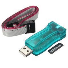
(from Wikipedia) In-system programming (ISP), also called in-circuit serial programming (ICSP), is the ability of some programmable logic devices, microcontrollers, and other embedded devices to be programmed while installed in a complete system, rather than requiring the chip to be programmed prior to installing it into the system. To program thee chip, you need some piece of HW.. named an ISP programmer. Here is an example of an ISP programmer:
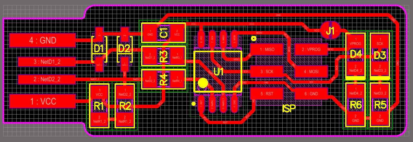
(from this site) The FabISP is an in-system programmer for AVR microcontrollers, designed for production within a FabLab. That is, it allows you to program the microcontrollers on other boards you make, using nothing but a USB cable/port and 6-pin IDC to 6-pin IDC cable. It's based on the USBtiny and V-USB firmwares, which allow the ATtiny44 to perform USB communication in software.
(from this site) There are multiple models of Fab ISPs. The one I decided to produce is the "Brian" version. Her e is how it looks like:
And here is how it looks like once everything is in place, I'm proud of it !!
How to get G-code from a PNG file
The traces, outcut, .. obtained from your CAD SW are typicaly PNG files (images). You need to process them to create G-code (i.e machine specific instructions) that will be executed by the mill to engrave the traces, dig the holes or cut the external limits of your PCB. There are many ways to achieve this but I choose Fab Lab Mods. Here is a typical workflow:
Using a CNC to mill a board
I wrote down some detailed documentation on how to use the mini-mill, with all the steps required to produce someting like this:
The main steps are:
- Create of get the circuit board traces, outcut and holes drill. Process them to get G-code (rml files)
- Prepare the SRM-20 : fix a sacrifical board, level it, install a 1/64 endmill and set the origin
- Mill the PCB by executing the G-code
- Inspect PCB, clean it with soap and water
A faced one minor issue. The cut was not deep enough and I was unable to detach the PCB. Instead of going back to the MODS, I just updated the RML file and set the Z parameter to -200 (i.e 2 mm deep)
Alternative - How to UV a PCB
Another way to produce PCBs is described here. I did not try it but it looks it requires a lot of chemicals (with all the consequences for your health and the environment. Now I understand why the CNC way is better.
Alternative - How to vinyl-cut a PCB
I really missed time to try this. I will come back later and give it a try for sure.
Getting and placing components
Here are the steps:
- Get your BOM (build of material for your project
- Prepare a sheet of paper with a label for each type of component and some double face type to glue them temporary to. Components are small and some of them are not marked
- Check and check again EACH compononent labeling when you get them out of Fab Lab inventory. When possible, double check if the marking fit with the label on the bin or platic bag. Someone could has put the wrong stock on the wrong place.
- Get one component at a time and solder it. Do not get all the components in one shot, there are hard to read and some of them have NO marking.
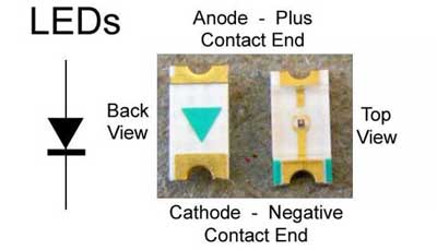
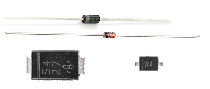
- Pay attention to polarity. Some components cannot be reversed

Soldering components
To start, let's summarize the 3 methods we could use to solder our components
- Manual (using an iron)
- Using an oven
- Using a wave
Check this video for a detailed explanation of the 3 methods. As explained in the video, the board designer has to take into account what process will be used in the manufacture. For a double side PCB and a reflow process for example, you should put the heavier components on one side
Soldering components manualy
I tried manual soldering. It is not easy but you learn fast (as fast as you burn your fingers ..).
Use flux ! and check some tutorials before, like this one. I followed Brian's tutorial, starting with the MCU, then components around and finaly the 6 pins header. Once completed, I read some comment arguing that the 6 pin header should be placed first because it is hard to solder at the end. Those are good comments..
Soldering using a reflow oven
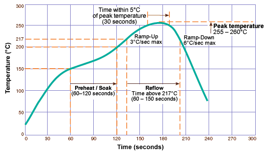
Reflow looks not so complex but the temperature has to be precisely controlled to get a clean result without toasting the components. I found a DIY source here to build a reflow oven and I'm in the process of building it. I will link pictures when it will be completed.
Soldering using a wave
Wave is totaly out of reach , this required big and expensive equipment. I visited a manufacture in China 5 years ago and I saw one of those machines. It is amazing how quick the PCB goes over the metal wave and literaly sucks just enough material to fix the componenents at the right place.

Checking PCB
Here is my check list (to be processed step by step - stop when not ok and fix the problem before going ahead
- Check your board against the schematic and PCB layout image to make sure that you have installed the correct components in the correct locations and orientations. Polarity is critical and there is no UNDO in electronics. I failed my first try because I did not pay attention to the tiny white line or the zener diodes
- Inspect your board visually. Components should be flat on the board, not tilted with pins in the air. Solder connections should be smooth, and solder should have flowed both onto the pin and onto the pad. If you still see a lot of exposed copper on the pad, or the solder is lumpy and draws up into a point where you removed the iron, you probably don't have a good connection. Reflow by applying heat and flux (either from a flux pen or by adding a tiny bit more solder). Also look for unwanted solder bridges between nearby traces and pins.
- Use a multimeter to check for shorts between VCC and GND BEFORE giving the burden to your PC to deal with it !
- Board is connected to an USB extension, not directly to your computer (to avoid permanent dammage to computer USB port if someting goes wrong
- Connection to USB is not loose. Add a additionnal layer of plastic if needed.
- Red LED turn On when you power up the board by connecting the USB extension to your computer
- If computer complains about a USB device drawing too much power, unplug the board and check for shorts.
Programming a PCB
But we are designing a PCB programmer, isn't it ?? Yes... but yo know the chicken and egg story... and we need to start somewhere. So.. I bought a chicken... oups.. an USB ASP
The connector on the left matches the PCB 6 pins header. The USB connector on the right goes to the computer.

Here are the steps:
-
Build the firmware (i.e the binaries that will resides on the MCU and runs there.. forever. To do this, we need first to change the makefile to set the right ISP type (the one I own is a usbASP
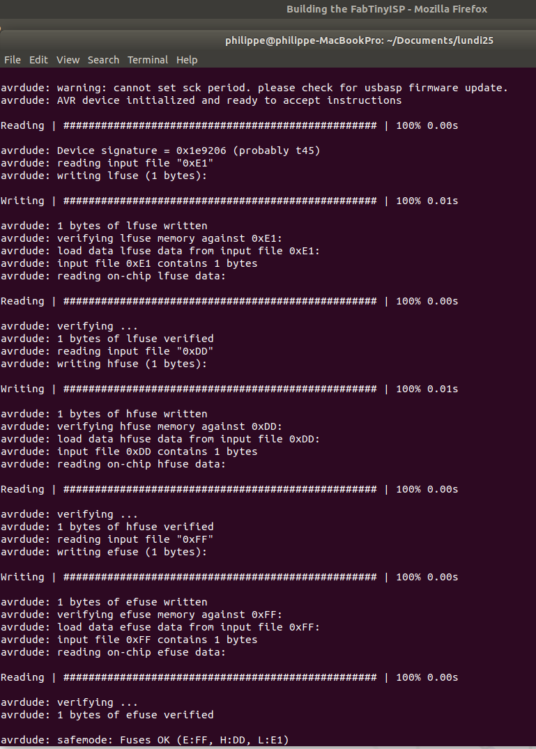
We need to set the fuses as well, still in the makefile. Wow... what are you talking about, you totaly con-fuse-d me ! What are "lock/fuse bits" ?
Everyone (well, not me..) knows that AVR MCUs have, in general, three memory areas: FLASH, which is dedicated to program code, SRAM for run-time variables and EEPROM, which can be used by user code to store data that have to be preserved when MCU is turned off. Now, the lock/fuses form a fourth memory area available for programming. This holds a few bytes that contain those bits. For example, ATmega48 has four of them – one byte for lock bits and three bytes for fuses: low, high and extended. What are those bits for? All MCU programmers are familiar with the fact that configuration of peripheral modules is done by setting or clearing some bits in appropriate registers. So the bytes with lock bits and fuses can be thought of as a sort of peripheral configuration registers, determining some very general system settings, like memory access, clock source and divider, start-up options, programming options and so on.
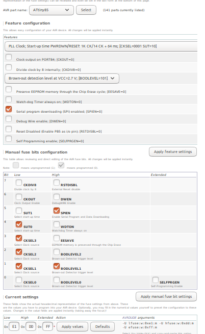
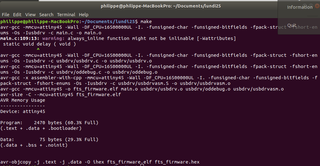
Once the makefile is updated, just type make to build the binaries
-
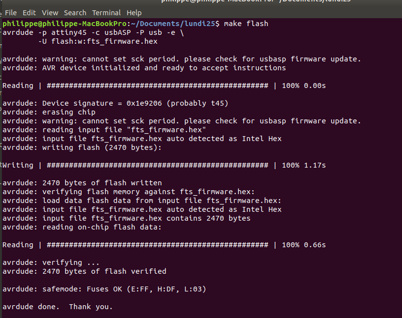
Flash the MCU, i.e connect your commercial ISP to your computer (USB) on one side and to the targeted MCU (i.e the 6 pin header of your board) on the other side and then type make flash
Just in case something could go wrong, here is my check list (to be processed step by step - stop when not ok and fix the problem before going ahead
- The newly created board is NOT connected to your computer
- Makefile updated as per the targeted AVR and the programmer (usbasp in my case)
- The programmer is connected correctly and pin 1 on the connector matches up to pin 1 on the board
- AVR programmer IS connected to your computer
- This tool could be usefull as well if you are more a UI style guy than a command line style guy
- See this to get more info on avrdude
- A little bit off track but you never know: a set of cores to support various mcu using Arduino IDE
-
Blow the fuses, still with your commercial ISP connected to your computer (USB) on one side and to the targeted MCU (i.e the 6 pin header of your board) on the other side. Type make fuses
Testing the program
To test your piece of art, unplug the commercial ISP (both sides) and connect your PCB to your computer (we have been told to use a USB extension to preserve the PC USB plugs. Under Linux, if you type dmseg> and lsusb you should see something like this

But the problem is I didn't... Here is what I got
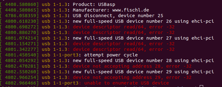
Then I spent more than 1 week trying to figure out what was wrong. I heard some other students had the same issue.. but with a different design (not the one from Brian, not even with a ATtiny85). For the benefit of future students, here are my research assumptions and the outcomes:
Assumption #1 : I did something wrong ! I checked again all components (value , marking). I measured the VCC, I checked whether there could be any short. I tested all lines using an ohmmeter. Nada ..
Assumption #2 : There is an issue with the design (when using a ATTiny85)! I found at least another student who made it. Shame on me !
Assumption #3 : There is an issue with the code ! I checked the changes (basicaly the MCU model and the fuses). I tried some alternate solutions to calibrate the oscillator. I checed all dependencies and I confirmed eveything was identical, at least to what has been demonstrated last year
Assumption #4 : There is an issue with the components ! My classmates have similar issues but with different components. There is a very small chance that we all faced the same defective components. But, anyway, I build a complete new experiment on a breadboard with throuh hole components. I managed to find all of them BUT the ATTiny85. I mounted the SMD one on a socket to make it fit the breadboard.
After many attempts, one of my set of 3 ATtiny85 was bricked and I was not able to flash it anymore, not even to detect it. I found a way to recover it. The design is the following. The wires on the left are connected to a 12v DC supply and the entire process is explained here
Assumption #5 : the design is supposed to be a 1.0 USB device. But why is it detected as a "full speed USB" (see the logs) ? It ended up as dead end but at least I know from now how it works . The detection relies on those two resistors between D- and VBUS. The original USB 1.0 specification, which was introduced in January 1996, defined data transfer rates of 1.5 Mbit/s Low Speed and 12 Mbit/s Full Speed.
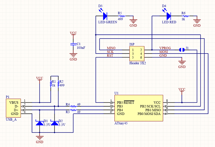
Assumption #? : I don't know... I asked a buddy for advices ...
Wow! I definitely need someone more knowledgeable ... I asked my instructor to have a look on it and we also asked the Fab Academy community for advices. See this forum
We finaly managed to make it work. The problem was a component.
 This is the one you should order
 And here is te final result (this time I used ATTINY45V but the problem was identical with ATTINY85)

Making things permanent
Two steps here: one on the software side, still with your commercial ISP connected to your computer (USB) on one side and to the targeted MCU (i.e the 6 pin header of your board) on the other side. Type make rstdisbl and the other one on the HW side: you have to cut the trace on the top right side, where there is a spot of solder (or a 0 ohm resistor)
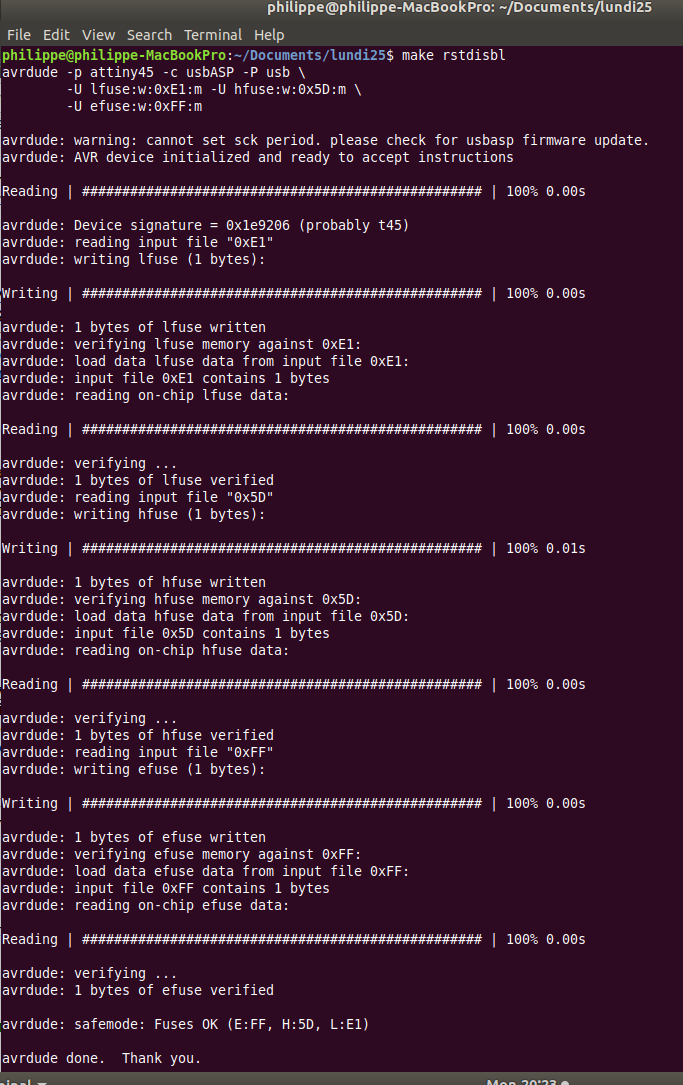
Testing the final product
From now, you should be able to use your ISP to flash new ISPs... Stay tuned...
Achievements
#1 (group) - Characterize the design rules for your PCB production process
Capstone
#1 -Capstone PCB (first try)
I had in mind to produce a first draft but I totaly missed time this week and I don't have (yet) the knowledge for the circuit design. Stay tuned...