
Electronics design
Introduction
For this week we had to:
1. use the test equipment in our lab to observe the operation
of a microcontroller circuit board
2. redraw the echo
hello-world board,
3. add (at least) a button and LED (with current-limiting resistor)
4.check the design rules, make it, and test it
extra credit: simulate its operation
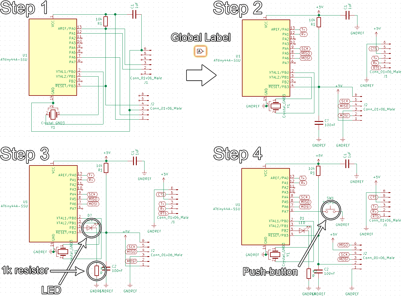
Redrawing the echo hello-world board.
I wanted to compare KiCad vs Eagle. The only thing I learned was that KiCad is free and open source and that Eagle has a free limited version (2 schematic sheets 2 signal or plane layers 80 cm2 (12.4 in2) board area) and a paid full version. I found this kicad-vs-eagle-2018-comparison very helpful it compares them in detail. My conclusion was that both Eagle and KiCad are similar. KiCad has hotkeys which are extremely useful, also it has a 3D Viewer and finally it's free and without limitations, so I decided to go with KiCad. I found this 5min tutorial very helpful to start with.
The next step was to build the circuit and connect the components. At first I was connecting the nods directly with wires and after several nods it was becoming an Gordian knot. After some research I found Connect pins with KiCad Bus, Labels, and Global Labels article very helpful. And in a minute my schematic transformed from a messy knot to a friendly circuit. Next I added an LED with a 1k current-limiting resistor, and a push-button.
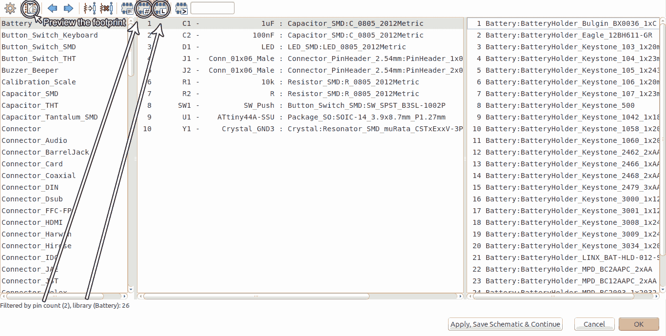
Next step was to annotate the schematic (The annotator will automatically annotate components) and assign footprints (we must associate schematic components to footprints) select each component and select the footprint you want for that component. Make sure two buttons shown in the image below are selected they filter the footprints by library and by pin count. After assigning all the footprints hit "Apply, Save Schematic & Continue" and hit "OK"
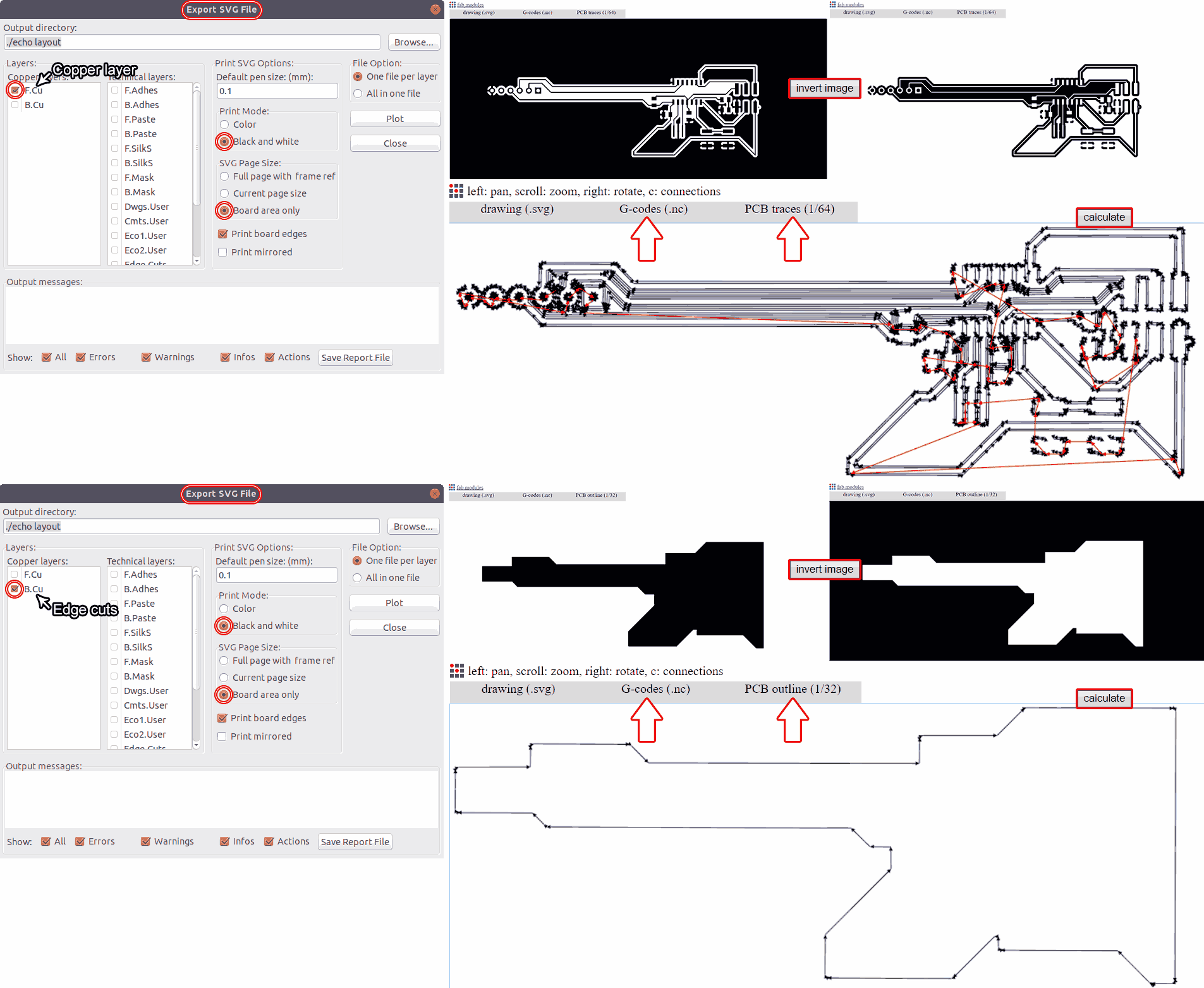
Now it's time to generate the netlist we need netlist to connect schematics diagram to PCB design layout, it contains information about what pin is connected where and what are the footprints. After this step find the "PCB editor" shown in the image below.

Next is to read the netlist file from PCB editor, arrange the layout and connect the pins.
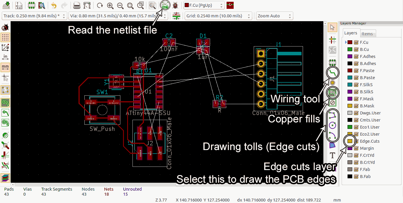
One important thing are Decoupling Capacitors, they should always be located as close as possible to an IC. The further away they are, they less effective they'll be. After playing and trying to layout the components I noticed a similarity of one of the 6 pin headers to a guitar tuning keys so I thought why not my PCB might have a shape of a guitar. I concluded that making the surface of this PCB as GND makes the wiring process much easier in order to do that you need "Copper fills" tool. Here is a good tutorial for Adding GND and VCC copper fills and you can see "Copper fills" tool in the image above.
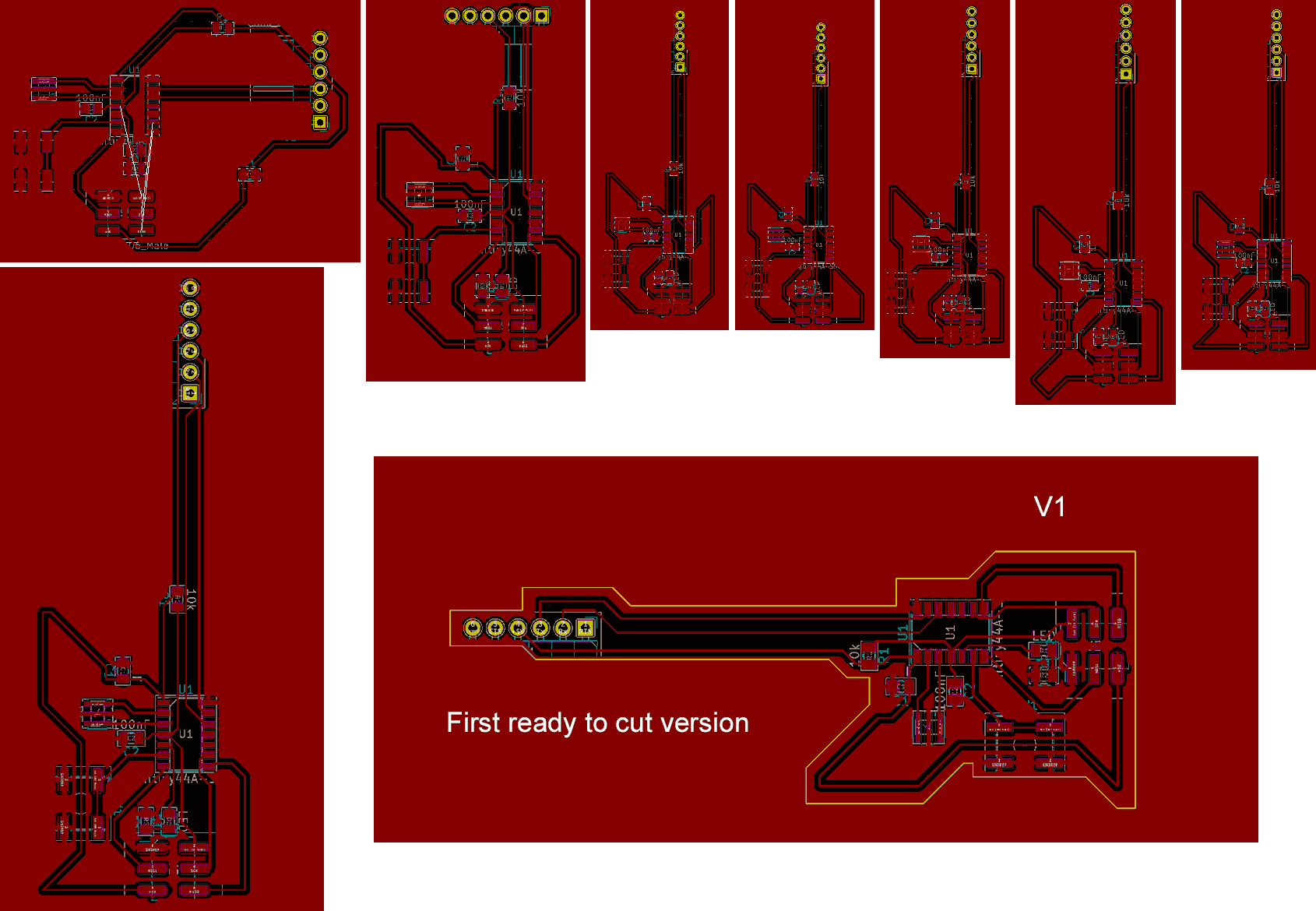
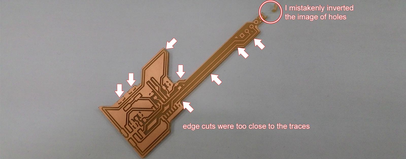
Cutting the guitar V1
I exported my board layout from PCB editor to SVG. I did this board with 3 different SVG's:
one for copper traces
one for edge cuts
one for holes (Holes should be done before cutting the edges)
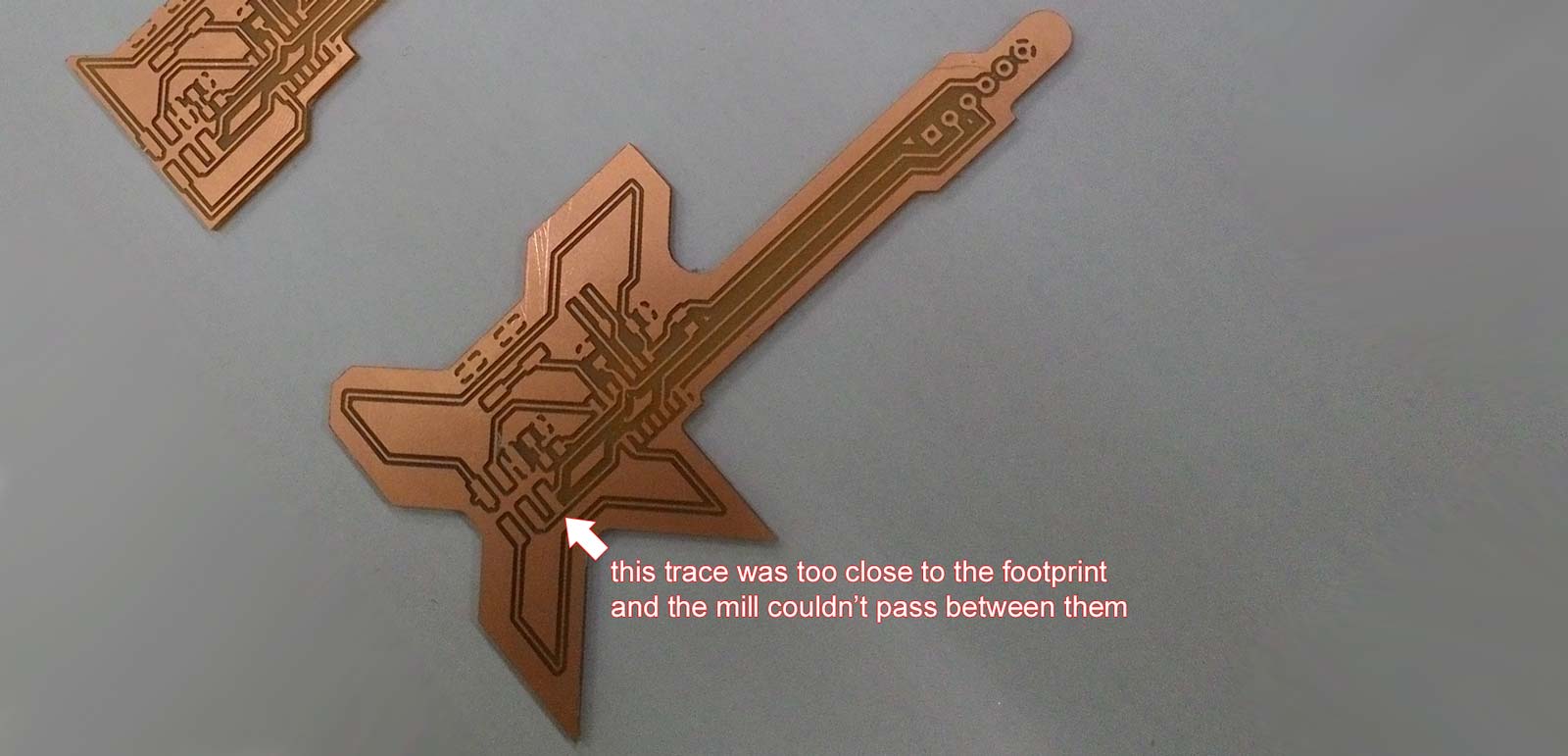
After finishing the second version I realized I could do that with just two:
one for copper traces
one for edge cuts and holes
Then I used Fabmodules to create G-codes. You can
find detailed steps on how to use Fabmodules to make PCB's in my week5.
After cutting the board I realized that the edge cuts were too close to the traces and some of the traces were damaged. I exported the holes in DRL format but couldn't use them with fabmodules so I decided to cut the holes instead of drilling them. I mistakenly inverted the image of holes before generating the G-code, so I got bigger holes and my board was completely damaged.
In the second version I increased the spaces between traces and the edge cuts, also I've changed the shape a little bit to make it look like an X, and brought one of decoupling Capacitors closer to the microcontroller.
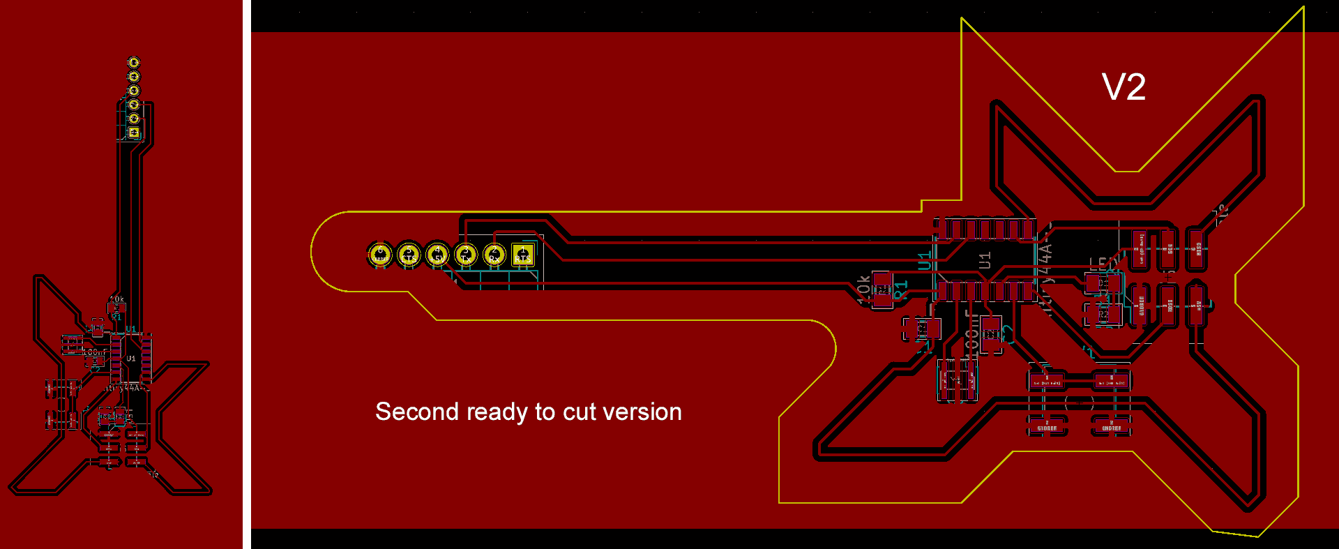
Here is the version 2
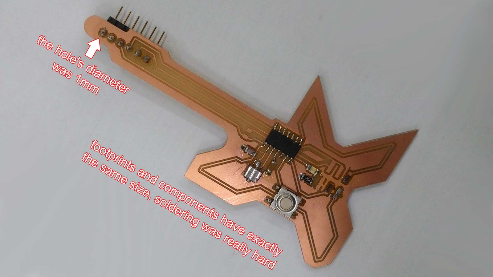
While soldering the components I noticed that footprints have exactly the same size as the components and it makes solder really hard. Also the hole's diameter was 1mm and the pinheaders we were using were 2mm (I found other pinheaders that fited and soldered them)
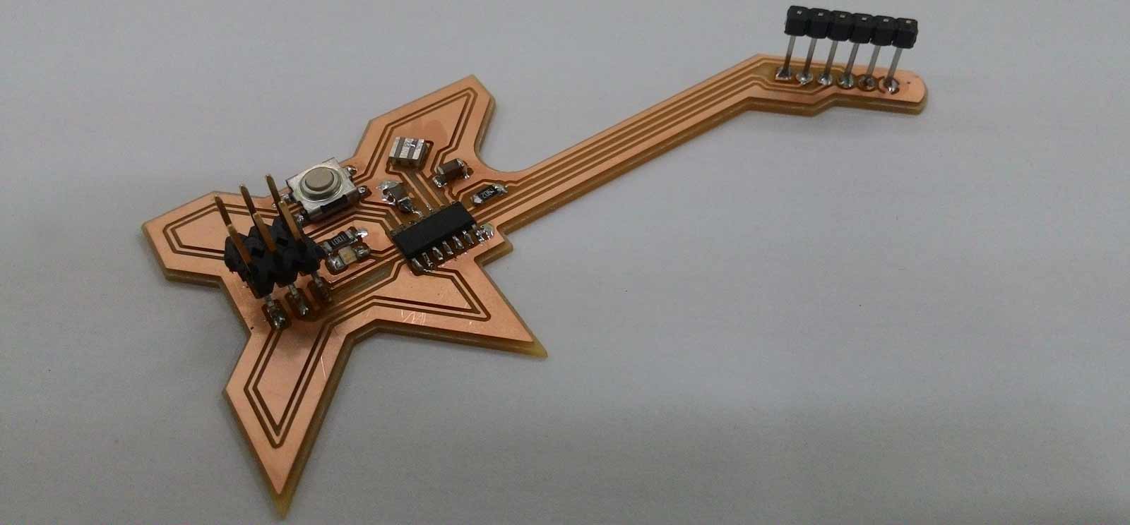
After soldering the components I realized that the footprints for resistors, capacitors and LED are very small, also the footprints and the holes for 6 pinheaders on the tail of the guitar were small too. I decided to make another version and fix this issues. I milled and soldered 3 more versions after I finally got this one V5.
Here is the version 5
Here are the SVG files of version 5:
Traces V5
Holes V5
Cutout V5
Here are KiCad files:
echo V5
Update
I couldn't know exactly why my guitar couldn't be programmed, but my final guess is that making the board surface as ground is not a good idea if you are not skilled. So I made another final version that connects ground pins with tracks.
Here are the SVG files of version 6:
Traces V6
Holes V6
Cutout V6
Here are KiCad files:
guitar V6